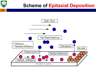
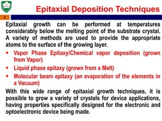
Epitaxial Deposition
Abu Syed Md. Jannatul Islam
Lecturer, Dept. of EEE, KUET, BD
1
Department of Electrical and Electronic Engineering
Khulna University of Engineering & Technology
Khulna-9203
2
Epitaxy
 The term Epitaxy comes from the
Greek word meaning ‘ordered
upon’.
 Epitaxy means the growth of a
single crystal film on top of a
crystalline substrate.
 For most thin film applications
(hard and soft coatings, optical
coatings, protective coatings) it is
of little importance.
 However, for semiconductor thin
film technology it is crucial.
3
Homoepitaxy:
 The film and the substrate are the same material.
 Often used in Si on Si growth (A on A)
 Epitaxially grown layers are purer than the substrate and can be doped
independently of it.
Types of Epitaxy
Heteroepitaxy:
 Film and substrate are different materials.(Growth of AlAs on Si or GaAs
on Si).
 Trying to grow a layer of a different material on top of a substrate leads to
unmatched lattice parameters.
 This will cause strained or relaxed growth and can lead to interfacial
defects.
 Such deviations from normal would lead to changes in the electronic,
optic, thermal and mechanical properties of the films.
 Allows for optoelectronic structures and band gap engineered devices.
4
Ordered, crystalline growth
Epitaxial growth
Epitaxial Growth
NOT epitaxial
 High Quality Film (1μm or less
thickness) deposited on a high
quality substrate.
 To ensure high crystalline quality,
the lattice parameters of the thin
layer should match with that of the
substrate (to minimize strain).
5
 While Si is not the ideal material from an electronic and optical point of view, its
abundance, ease of processing and availability of a good native oxide have made it
the backbone of semiconductor industry.
 Combining Si substrates with compound semiconductor films would enable higher
optoelectronic functionality and higher speeds. However, there are severe lattice
mismatch and chemical compatibility issues between Si and most III-V alloys that
preclude direct growth.
 Metal-Semiconductor Hetero-epitaxy: Metal-semiconductor structures are used for
contact applications. While not essential, epitaxial growth allows increased electron
mobility through a junction.
 Epitaxial growth is useful for applications that place stringent demands on a
deposited layer:
 High purity, Low defect density, Abrupt interfaces, Controlled doping profiles
 High repeatability and uniformity, Safe, efficient operation
 Can create clean, fresh surface for device fabrication
Why Epitaxial Growth
6
 Engineered wafers
 Clean, flat layer on top of less ideal
Si substrate
 On top of SOI structures
 Ex.: Silicon on sapphire
 Higher purity layer on lower quality
substrate (SiC)
 In CMOS structures
 Layers of different doping
 Ex. p- layer on top of p+ substrate to
avoid latch-up
Why Epitaxial Growth
 To make layer which is not available in nature
 Very important in III-V semiconductor production
 Bipolar Transistor (Needed to produce buried layer)
 III-V Devices (Interface quality key, Hetero-junction
Bipolar Transistor, LED, Laser).
7
Steps:
 Absorption of ad atoms
 Surface diffusion
 Crystal growth
 Evaporation of adatoms
Parameters:
 Growth temperature
 Growth pressure
 Flow amount of reactants
 Substrate and treatment
Epitaxial Growth Steps & Parameters
8
Scheme of Epitaxial Deposition
9
Epitaxial Deposition Techniques
Epitaxial growth can be performed at temperatures
considerably below the melting point of the substrate crystal.
A variety of methods are used to provide the appropriate
atoms to the surface of the growing layer.
 Vapor Phase Epitaxy/Chemical vapor deposition (grown
from Vapor)
 Liquid phase epitaxy (grown from a Melt)
 Molecular beam epitaxy (an evaporation of the elements in
a Vacuum)
With this wide range of epitaxial growth techniques, it is
possible to grow a variety of crystals for device applications,
having properties specifically designed for the electronic and
optoelectronic device being made.
10
Liquid Phase Epitaxy
 Reactants are dissolved in a molten solvent at high temperature
 Substrate dipped into solution while the temperature is held
constant
 Example: SiGe on Si
 Bismuth used as solvent
 Temperature held at 800°C
 High quality layer
Molecular Beam Epitaxy
 Very promising technique
 Beams created by evaporating solid source in UHV
 Not ideal for large area layers or abrupt interfaces
 Thermodynamic driving force relatively very low
Epitaxial Deposition Techniques
11
 MOMBE---means when Metel Organic Source used for MBE
 Sputtering---the layer quality is very poor. Thus it is used for making
contact with the help of metal related source.
 HVPE---Hydride Vapor Phase Epitaxy
 Pulse laser Deposition (PLD)
 Reactive Evaporation
 Electron Beam Plasma Technique
 Solvo thermal Method
Epitaxial Deposition Techniques
*Advantages, Disadvantages, and Applications of all these
techniques are very much important. Please collect all the
information……………….
12
Techniques Strengths Weaknesses
LPE (liguid phase epitaxy) Simple, High purity Scale economies Inflexible,
Non-uniformity
HVPE( hydride vapor
phase epitaxy)
Well developed Large scale No Al alloys Complex
process/reactor control difficult,
Hazardous sources
MBE Simple process, Uniform,
Abrupt interface In-situ
monitoring
As/P alloy difficult, Expensive ,
Low throughput
MOCVD/OMVPE/OMCVD
MOVPE
Most flexible, Large scale
production Abrupt interface
Simple reactor, High purity,
selective in situ monitoring
Expensive sources Most
parameters to control Accurately
Hazardous precursors
Overview of Epitaxy Techniques

Epitaxy, Epitaxial Growth--ABU SYED KUET

  • 1.
    Epitaxial Deposition Abu SyedMd. Jannatul Islam Lecturer, Dept. of EEE, KUET, BD 1 Department of Electrical and Electronic Engineering Khulna University of Engineering & Technology Khulna-9203
  • 2.
    2 Epitaxy  The termEpitaxy comes from the Greek word meaning ‘ordered upon’.  Epitaxy means the growth of a single crystal film on top of a crystalline substrate.  For most thin film applications (hard and soft coatings, optical coatings, protective coatings) it is of little importance.  However, for semiconductor thin film technology it is crucial.
  • 3.
    3 Homoepitaxy:  The filmand the substrate are the same material.  Often used in Si on Si growth (A on A)  Epitaxially grown layers are purer than the substrate and can be doped independently of it. Types of Epitaxy Heteroepitaxy:  Film and substrate are different materials.(Growth of AlAs on Si or GaAs on Si).  Trying to grow a layer of a different material on top of a substrate leads to unmatched lattice parameters.  This will cause strained or relaxed growth and can lead to interfacial defects.  Such deviations from normal would lead to changes in the electronic, optic, thermal and mechanical properties of the films.  Allows for optoelectronic structures and band gap engineered devices.
  • 4.
    4 Ordered, crystalline growth Epitaxialgrowth Epitaxial Growth NOT epitaxial  High Quality Film (1μm or less thickness) deposited on a high quality substrate.  To ensure high crystalline quality, the lattice parameters of the thin layer should match with that of the substrate (to minimize strain).
  • 5.
    5  While Siis not the ideal material from an electronic and optical point of view, its abundance, ease of processing and availability of a good native oxide have made it the backbone of semiconductor industry.  Combining Si substrates with compound semiconductor films would enable higher optoelectronic functionality and higher speeds. However, there are severe lattice mismatch and chemical compatibility issues between Si and most III-V alloys that preclude direct growth.  Metal-Semiconductor Hetero-epitaxy: Metal-semiconductor structures are used for contact applications. While not essential, epitaxial growth allows increased electron mobility through a junction.  Epitaxial growth is useful for applications that place stringent demands on a deposited layer:  High purity, Low defect density, Abrupt interfaces, Controlled doping profiles  High repeatability and uniformity, Safe, efficient operation  Can create clean, fresh surface for device fabrication Why Epitaxial Growth
  • 6.
    6  Engineered wafers Clean, flat layer on top of less ideal Si substrate  On top of SOI structures  Ex.: Silicon on sapphire  Higher purity layer on lower quality substrate (SiC)  In CMOS structures  Layers of different doping  Ex. p- layer on top of p+ substrate to avoid latch-up Why Epitaxial Growth  To make layer which is not available in nature  Very important in III-V semiconductor production  Bipolar Transistor (Needed to produce buried layer)  III-V Devices (Interface quality key, Hetero-junction Bipolar Transistor, LED, Laser).
  • 7.
    7 Steps:  Absorption ofad atoms  Surface diffusion  Crystal growth  Evaporation of adatoms Parameters:  Growth temperature  Growth pressure  Flow amount of reactants  Substrate and treatment Epitaxial Growth Steps & Parameters
  • 8.
  • 9.
    9 Epitaxial Deposition Techniques Epitaxialgrowth can be performed at temperatures considerably below the melting point of the substrate crystal. A variety of methods are used to provide the appropriate atoms to the surface of the growing layer.  Vapor Phase Epitaxy/Chemical vapor deposition (grown from Vapor)  Liquid phase epitaxy (grown from a Melt)  Molecular beam epitaxy (an evaporation of the elements in a Vacuum) With this wide range of epitaxial growth techniques, it is possible to grow a variety of crystals for device applications, having properties specifically designed for the electronic and optoelectronic device being made.
  • 10.
    10 Liquid Phase Epitaxy Reactants are dissolved in a molten solvent at high temperature  Substrate dipped into solution while the temperature is held constant  Example: SiGe on Si  Bismuth used as solvent  Temperature held at 800°C  High quality layer Molecular Beam Epitaxy  Very promising technique  Beams created by evaporating solid source in UHV  Not ideal for large area layers or abrupt interfaces  Thermodynamic driving force relatively very low Epitaxial Deposition Techniques
  • 11.
    11  MOMBE---means whenMetel Organic Source used for MBE  Sputtering---the layer quality is very poor. Thus it is used for making contact with the help of metal related source.  HVPE---Hydride Vapor Phase Epitaxy  Pulse laser Deposition (PLD)  Reactive Evaporation  Electron Beam Plasma Technique  Solvo thermal Method Epitaxial Deposition Techniques *Advantages, Disadvantages, and Applications of all these techniques are very much important. Please collect all the information……………….
  • 12.
    12 Techniques Strengths Weaknesses LPE(liguid phase epitaxy) Simple, High purity Scale economies Inflexible, Non-uniformity HVPE( hydride vapor phase epitaxy) Well developed Large scale No Al alloys Complex process/reactor control difficult, Hazardous sources MBE Simple process, Uniform, Abrupt interface In-situ monitoring As/P alloy difficult, Expensive , Low throughput MOCVD/OMVPE/OMCVD MOVPE Most flexible, Large scale production Abrupt interface Simple reactor, High purity, selective in situ monitoring Expensive sources Most parameters to control Accurately Hazardous precursors Overview of Epitaxy Techniques