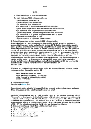
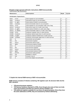
1. MPMC
Unit 5
1. State the features of 8051 microcontroller.
The main features of 8051 microcontroller are:
1) 8051 have 128 bytes of RAM
2) 8051 have 128 user defined flags
3) it consist of 16 bit address bus
4) it also consist of 3 internal and two external interrupts
5) less power usage in 8051 with respect to other micro-controller
6) it consist of 16-bit program counter and data pointer
7) 8051 can process 1 million one-cycle instructions per second
8) it also consist of 32 general purpose registers each of 8 bits
9) ROM on 8051 is 4 Kbytes in size
10) it also consist of Two 16 bit Timer/ Counter
2. Explain the operation of stack pointer in 8051 microcontroller.
The stack pointer (SP) is an 8-bit register at location 81H. A stack is used for temporarily
storing data. It operates on the basis of last in first out (LIFO). Putting data onto the stack is
called "pushing onto the stack" while taking data off the stack is called "popping the stack."
The stack pointer contains the address of the item currently on top of the stack. On power-up
or reset the SP is set to 07H. When pushing data onto the stack, the SP is first increased by
one and the data is then placed in the location pointed to by the SP. When popping the stack,
the data is taken off the stack and the SP is then decreased by one. Since reset initialises the
SP to 07H, the first item pushed onto the stack is stored at 08H (remember, the SP is
incremented first, then the item is placed on the stack). However, if the programmer wishes to
use the register banks 1 to 3, which start at address 08H, he/she must move the stack to
another part of memory. The general purpose RAM starting at address 30H is a good spot to
place the stack. To do so we need to change the contents of the SP.
MOV SP, #2FH.
3.Write an 8051 assembly language program to add two 8 bits number data stored in internal
memory and store the result in register R2.
MOV A,#44;LOAD ACC WITH 44H
ADD A,#66;ADD 66H WITH THE CONTEN
MOV R2,A;MOVE RESULT IN REGISTER
HERE: SJMP HERE
4. Explain register bank?
Register banks in the 8051
As mentioned earlier, a total of 32 bytes of RAM are set aside for the register banks and stack.
These 32 bytes are divided into 4 banks of registers in which
each bank has 8 registers, RO – R7. RAM locations from 0 to 7 are set aside for bank 0 of RO –
R7 where RO is RAM location 0, Rl is RAM location 1, R2 is location 2, and so on, until memory
location 7, which belongs to R7 of bank 0. The second bank of registers RO – R7 starts at RAM
location 08 and goes to location OFH. The third bank of RO – R7 starts at memory location 10H
and goes to loc ation 17H. Finally, RAM locations 18H to 1FH are set aside for the fourth bank
of RO – R7. The following shows how the 32 bytes are allocated into 4 banks:
1. Microcontroller having inbuilt RAM or ROM and inbuilt timer.
2. Input and output ports are available.
3. Inbuilt serial port.
4. Separate memory to store program and data.
5. Many functions pins on the IC.
6. Boolean operation directly possible.
1
2. MPMC
7. It take few instructions to read and write data from external memory.
5.Compare microprocessor and microcontroller.
Microprocessor Microcontroller
1. Do not have inbuilt RAM or ROM and timer. 1. Microcontroller having inbuilt RAM or ROM
and inbuilt timer.
2. Input and output ports are not available,
requires extra device like 8155 2. Input and output ports are available.
3. Do not have inbuilt serial port, requires 8250 3. Inbuilt serial port.
device.
4. Program and data are stored in same memory. 4. Separate memory to store program and data.
5. Less multifunction pins on IC. 5. Many functions pins on the IC.
6. Boolean operation is not possible directly. 6. Boolean operation directly possible.
7. It take many instruction to read and write data 7. It take few instructions to read and write data
from external memory. from external memory.
2
3. MPMC
6.Explain single operand arithmetic instructions of8051microcontroller
7. Explain the internal RAM memory of 8051 microcontroller.
RAM memory consists of 3 blocks containing 128 registers each. Its structure falls into the
8051 standard:
128 general-purpose registers;
128 memory locations reserved for SFRs. Even though only some of them are trully
used, free locations shouldn’t be used for storing variables; and
128 additional registers available for use (have no special purpose). Since they have
the same addresses as SFRs, they are accessed by indirect addressing.
3
4. MPMC
8. Can you use DPTR to access internal ROM? Justify your answer.
DPTR register is not a true one because it doesn't physically exist. It consists of two separate
registers: DPH (Data Pointer High) and (Data Pointer Low). For this reason it may be treated as
a 16-bit register or as two independent 8-bit registers. Their 16 bits are primarly used for
external memory addressing. Besides, the DPTR Register is usually used for storing data and
intermediate results.
9. Write an 8051 assembly language program to perform BCD addition of two 8 bit number data
stored in location 51H and 52H and store the result in memory location 53H.
MOV R1,#20
MOV R2,#30
MOV A,R1
ADD A,R2
DA R,A
MOV R5,A
HERE: SJMP HERE
4
5. MPMC
10. List and explain various data transfer instructions of 8051 microcontroller.
5