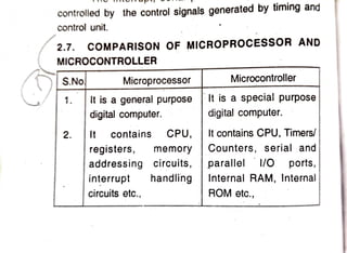
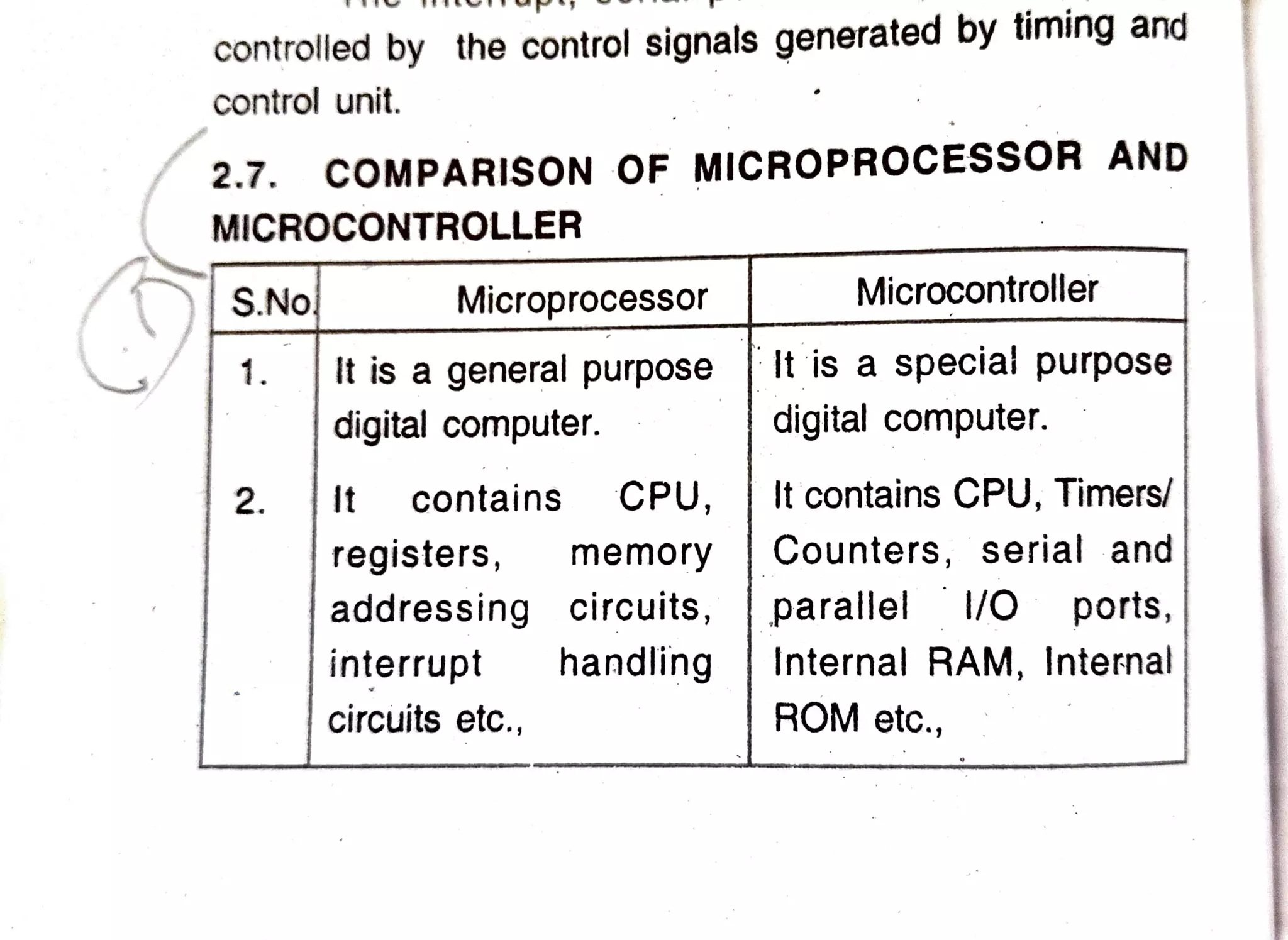
The document discusses different addressing modes of the 8051 microcontroller. It describes five addressing modes: immediate, register, direct, indirect, and index addressing modes. Immediate addressing uses a constant in the operand field. Register addressing accesses operands stored in registers. Direct addressing specifies the operand with an 8-bit address. Indirect addressing specifies a register containing the operand address. Index addressing accesses a look-up table using the accumulator and base register sum as the address.
The 8051 microcontroller is designed for real-time applications like industrial control and automobiles. It has features like interrupts, bit addressability, and an enhanced instruction set that make it powerful and cost-effective. The 8051 has 4KB of internal ROM, 128 bytes of internal RAM, 32 I/O lines, and can access up to 64KB each of external program and data memory. It has various special function registers that control timers, serial ports, and interrupts to interface with peripherals. The 8051's architecture includes a CPU, program memory, data memory, ports, and special function registers connected via an internal bus.
The 8051 microcontroller has 4KB of ROM, 128KB of RAM, and 4 ports with 32 I/O lines. This configuration satisfies the needs of most programmers for developing automation devices. The 8051 has two types of memory - program memory (ROM) for permanently storing programs and data memory (RAM) for temporarily storing data and results. The 8051 has special function registers used for running and monitoring the microcontroller, including registers for timer control, interrupt control, and serial communication.
The document discusses the memory organization and registers of the 8051 microcontroller. It describes the program memory and data memory, which are implemented using EPROM and RAM respectively. It then discusses the different registers of the 8051 including the accumulator, B register, data pointer register, stack pointer register, and special function registers. The special function registers are used for tasks like timer control and interrupt control.
The document discusses the 8051 microcontroller. It begins by describing the key features of the 8051 microcontroller, including that it has an 8-bit CPU, 4KB of internal program memory, 128 bytes of internal data memory, 32 I/O lines that can be used as ports, and two 16-bit timer counters. It then provides more details on the internal architecture, describing the ALU, registers, memory organization, and other components. It concludes by explaining features like the register banks and stack memory.
The document describes the 8051 microcontroller, its features which include 4 I/O ports, 2 timers, serial communication interface, and interrupts. It discusses the internal architecture such as memory organization, registers, and oscillator circuit. The document also provides details on the ports, timers, serial communication, and power modes of the 8051 microcontroller.
The document describes the 8051 microcontroller, its features which include 4 I/O ports, 2 timers, serial communication interface, and ability to address 64KB of external memory. It discusses the internal architecture of the 8051 including its oscillator, memory architecture with RAM and ROM, registers, ports, timers and interrupts. The 8051 is an 8-bit microcontroller originally developed by Intel with various features making it useful for embedded applications.
The document describes the internal architecture of the 89C52 microcontroller. It has the following on-chip facilities: 4k ROM, 128 byte RAM, one USRT, 32 I/O port lines, two 16-bit timers/counters, six interrupt sources, and an on-chip clock oscillator. Other family members have variations like 8k ROM, 256 byte RAM, and an extra timer/counter. The 89C52 architecture includes ports, memory, a CPU, and peripherals that allow it to interface with external devices.
The 8051 microcontroller has an 8-bit CPU, 64KB program memory, 64KB data memory, 4KB onboard program memory, 128 bytes onboard data RAM, 32 I/O lines, two 16-bit timers/counters, a full duplex UART, and a 6-source interrupt structure. It consists of a CPU, two memory sections, I/O ports, special function registers, and control logic connected via an 8-bit internal data bus. The 8051 has 40 pins, with some pins having alternate functions.
A microcontroller is a single-chip microprocessor system consisting of a CPU, memory, and input/output ports. It can be considered a complete computer on a single chip. The 8051 was an early microcontroller developed by Intel for use in embedded systems. It had 4KB of program memory, 128 bytes of data memory, timers, counters, and I/O ports. The 8051 has separate memory spaces for program and data memory and its CPU, registers, timers and I/O ports allow it to monitor and control external devices.
Pc based wire less data aquisition system using rf(1)Vishalya Dulam
This document provides an overview of a PC-based wireless data acquisition system using RF technology. It describes the system's hardware components, including the microcontroller, sensors, analog-to-digital converter, encoders, decoders, and transmitter and receiver modules. It also discusses the microcontroller architecture, memory types, registers, ports, and peripherals. Finally, it outlines the software tools and programming required to develop applications for the system.
SYBSC IT SEM IV EMBEDDED SYSTEMS UNIT III The 8051 MicrocontrollersArti Parab Academics
The 8051 Microcontrollers: Microcontrollers and Embedded processors, Overview of 8051 family. 8051 Microcontroller hardware, Input/output pins, Ports, and Circuits, External Memory. 8051 Programming in C: Data Types and time delay in 8051 C, I/O Programming, Logic operations, Data conversion Programs
The document discusses assembly language programming. It begins by explaining that assembly language is a low-level programming language useful for embedded systems and device drivers due to its close correspondence to machine code and ability to optimize for speed and size. The document then provides details on memory organization, addressing modes, interrupts, and an example program to test the program status word register in assembly language.
This document discusses the architecture and programming of the 8051 microcontroller. It begins by outlining the objectives and outcomes of studying the 8051. It then provides details on the basics of the 8051 architecture, including its internal blocks like RAM, registers, timers, ports, and memory organization. It also compares microcontrollers to general purpose microprocessors. Finally, it discusses the internal registers of the 8051 like the program counter, stack pointer, and special function registers in detail.
The document discusses the 8051 microcontroller, including its architecture, pins, ports, and memory organization. It provides details on the 8051's 8-bit CPU, registers, program memory, data memory, special function registers, and four 8-bit I/O ports. It also describes the functions of key pins for the crystal oscillator, reset, external access, and program store enable.
The document discusses microcontrollers and the 8051 microcontroller. It provides details about the internal architecture and components of the 8051 microcontroller, which includes a CPU, RAM, ROM, I/O ports, timers, and other special function registers. The 8051 is an 8-bit microcontroller commonly used in embedded systems due to its low cost and integration of components into a single chip.
BASIC INFORMATION OF ARCHITECTURE OF MICRO-CONTROLLER 8051 AS PER GTU SYLLABUS. Please Comment if u Like.. n Give u r feedback..
For More Information Go to
http://www.noesiseducation.blogspot.com
The document discusses the 8051 microcontroller. It provides details about the 8051 architecture such as its memory organization, I/O ports, registers, and instruction set. The key advantages of microcontrollers over microprocessors are that microcontrollers have peripherals integrated into a single chip, making the system design simpler and more reliable.
This document describes the architectural features and peripheral functions of the PIC16F873 microcontroller. It discusses the microcontroller core, which uses a Harvard architecture with separate program and data memory. It then describes the peripheral features including timers, I/O ports, serial communication interfaces, and analog-to-digital converter. Diagrams are included showing the memory map, pin configuration, and block diagrams of timers and serial communication modules. The document provides a detailed overview of the capabilities and operation of the PIC16F873 microcontroller.
The document compares microprocessors and microcontrollers and provides details about the 8051 microcontroller architecture. It describes that microcontrollers contain a microprocessor, memory, I/O interfaces and peripheral devices while microprocessors only contain an ALU, control unit and registers. It then provides details about the 8051 architecture such as its ports, registers, memory organization, and instruction set which includes data transfer, arithmetic, logical and I/O instructions.
The 8085 microprocessor has three main sections: the arithmetic and logic section containing an accumulator, temporary register, ALU, and flag register; the register section containing general purpose registers and special purpose registers like the program counter and stack pointer; and the control section which fetches and decodes instructions and controls timing. It has limitations like an 8-bit word length resulting in slow processing speed, limited addressing modes, and inability to access more than 64KB of memory.
A microprocessor is an electronic component that is used by a computer to do its work. It is a central processing unit on a single integrated circuit chip containing millions of very small components including transistors, resistors, and diodes that work together. Some microprocessors in the 20th century required several chips. Microprocessors help to do everything from controlling elevators to searching the Web. Everything a computer does is described by instructions of computer programs, and microprocessors carry out these instructions many millions of times a second. [1]
Microprocessors were invented in the 1970s for use in embedded systems. The majority are still used that way, in such things as mobile phones, cars, military weapons, and home appliances. Some microprocessors are microcontrollers, so small and inexpensive that they are used to control very simple products like flashlights and greeting cards that play music when you open them. A few especially powerful microprocessors are used in personal computers.
The document provides an overview of the 8051 microcontroller architecture. It discusses that the 8051 microcontroller incorporates features found in a microprocessor such as RAM, ROM, I/O ports, timers, and serial communication on a single chip. The 8051 has 128 bytes of RAM for data storage, 4KB of ROM for program storage, two 16-bit timers for generating delays, serial communication pins for transmitting and receiving data, and four 8-bit I/O ports. Selection criteria for a microcontroller in an embedded system include meeting computational needs efficiently and cost effectively based on factors like speed, memory size, I/O pins, and software development tools availability.
This presentation discusses the internal architecture of Intel 8051. It discusses basic families of 8051, the programmer view, register sets and memory organiszation of 8051
Fundamentals of Microcontroller 8051 by Dr. Jogade S M, Assistant Professor, ...sangeeta jogade
The document provides an overview of fundamentals related to microcontrollers including the 8051 microcontroller. It defines common terms like binary number, bit, byte, word, bus, register, integrated circuit, and microprocessor. It then discusses the 8051 microcontroller specifically, covering its memory organization, I/O ports, timers, interrupts, and special function registers. The document is intended as a revision guide for understanding basic microcontroller concepts centered around the popular 8051 microcontroller.
The document describes the architecture and components of an 8051 microcontroller. It includes details about the CPU registers like the accumulator, program status word, stack pointer, and timers. It describes the ports, interrupts, and memory organization. The special function registers control functions like timers, serial communication, and interrupts. The timers can be configured in different modes to generate time delays or count events. External memory can be accessed using address and data lines connected to the ports.
The document provides an introduction and overview of the Intel 8096 microcontroller. It discusses the 8096's salient features such as its 16-bit architecture, high-speed I/O capabilities, and uses in motor control and robotics. It describes the 8096's architecture including its 16-bit CPU, registers, memory mapping, and I/O features such as timers, serial port, and A/D converter. The document provides details on the 8096's instruction set, addressing modes, and interrupt structure.
Building a Raspberry Pi Robot with Dot NET 8, Blazor and SignalRPeter Gallagher
In this session delivered at NDC Oslo 2024, I talk about how you can control a 3D printed Robot Arm with a Raspberry Pi, .NET 8, Blazor and SignalR.
I also show how you can use a Unity app on an Meta Quest 3 to control the arm VR too.
You can find the GitHub repo and workshop instructions here;
https://bit.ly/dotnetrobotgithub
1. controlled by the control signals generated by timing and
control unit.
2.7. COMPARISON OF MICROPROCESSOR AND
MICROCONTROLLER
Microcontroller
S.No Microprocessor
1. It is a general purpose It is a special purpose
1
digital computer. digital computer.
It contains CPU, It contains CPU, Timers/
memory| Counters, serial and
addressing circuits,parallel 1/0 ports,
handlingInternal RAM, Internal
ROM etc.,
2.
registers,
interrupt
circuits etc.,
2. 2.08
3. It has many op-codes | It has one or two
op-codes for moving
3.
for moving data from
extenal memory to the data from external|
CPU. memory to the CPU.
It has one or two bit
handling instructions.
It has many bit handling
instructions.
To function as computer,
4.
To function as computer,
5
it needs additional it does not need any
external parts. external parts.
6 Examples: 8085,8086, Exampes: 8051,8048,
Z80 etc. 8052 etc.,
2.8.SIGNAL DESCRIPTION OF 8051
PLO
40cc
PI.I2 39 PO.0/ADO
P1.2 3 38PO.1/ADI
37P0.2/AD2
36P0.3/AD3
P13 4
P14 5
PI.5 6
P16 7
35PO4/AD4
34 P0.5/AD5
P1.7 8
RESET9
(RXD)P3.010 IC 8051 31 EAVPP
33PO.6/AD6
32PO.7/AD7
TXD)P3.1 30AL.E/PROG
INTO)P3.2 12
INTT)P3.3 13
29 PSEN
28 P2.7/A15
(TOP34 14
(TI)P3.5 15
(WRP3.6 16
27P2.6/A14
26P2.5/A13
25 P2.4/A12
(RD)P3.7 7
XTAL2 18
XTALI 19
s 20
24P2.3/A11
23P2.2/A10
22P2.1/A9
21P2.0/A8
Fig. 2.2 Pindiagram of 8051
3. 2.09
M i c r o c o n t r o l l e r
8051
is
a v a i l a b l e
in a 40 pin plastin
ceramic
DIP
p a c k a g e s .
The pin
diagram
of8051 is shou
a 40 pin plastic and
1 is show in
the fig.2.2.
b ) V s s :
It is a
return pin for the supply
(Ground).
b)
) V o c :
It is a +5Vsupply
voltage
pin.
a)
to reset the
c) m i c r o c o n t r o l l e r .
RESET:
The
reset pin is used to reset the
e
d
indicates that the valid address bits are available
their respective pins. This ALE signal is valid only for
external memory
accesses. This pin also act as
program pulse input during on-chip EPROM
programming.
d)ALE/PROG:Theaddress latch enable output pulse
on
e) EAVpp: External access pin, iftied low, indicates
that the 8051 can address external program memory.
For execution of programs in internal program
memory this pin must be tied high. This pin also
receives 21 Voits for programming the on-chip
EPROM.
PSEN: This program store enable pin is not activated
for internal fetches. It is activated when the CPU IS
accessing external program memory. PSEN I
activated twice every cycle.
g) Port0 (PO.0 P0.7): Port 0 acts as an 8"
bidirectional bit/byte addressable /O port. This ra
as
been allotted an
address in the SFR address rany
range
(ADa-AD) during external memory access.
also receives code bytes during
programming
Port 0 acts as
multiplexed address and data i
R address
ess and data line:
0
internal EPROM. the
4. h) Port 1(P1.0 -
P1.7): Port 1 acts as an 8-bit
h)
bidirectional bit/byte addressable port. It has been
allotted an address in the SFR address range.
i)Port 2 (P2.0 P2.7): Port2 acts as 8-bit bidirectional
bitbyte addressable l/O port. It has been allotted an
address in the SFR address range.
During external memory access, port 2 emits
higher eight bits of address (As - A15). Port 2 also
receives higher order address bits during
programming on the on-chip EPROM.
Port 3 (P3.0- P3.7): Port 3 is an 8-bit bidirectional bit/
byte addressable l/0 port. It has been allotted an
address in the SFR address range. The port 3 pins
also serve the alternate functions as listed in the table
below.
Port Pins Alternate Functions
P3.0 RXD (Serialinputport)
P3.1 TXD (Serial output port)
P3.2 INTO (External interrupt 0)
P3.3 INT1. (External interrupt 1)
P3.4 TO (Timer/Counter0 external input)
P3.5 T1 (Timer/Counter 1 external input)
P3.6 WR (External data memory write strobe)
P3.7 RD (External data memory read strobe)
5. 2.11
XTALI and XTAL2
There is an in-built oscillato.
which derives the necessary clock frequency for tha
operation of the oscillator. XTAL1 is the input to the
inverting oscillator amplifier. XTAL2 is the output from
the inverting oscillator amplifier.
ALLL
(ARITHMETIOAND LOCIR IAITV
6. Spaces.
2.11.1. ROM (Program memory)
Program memory can only be read, not written to.
There can be upto 64 Kbytes of program memory. In the
ROM and EPROM versions, the lowest 4 Kbytes are
provided on-chip. In the ROM less versions all program
memory is external (off-chip). The 64 Kbyte program memoiy
7. 2.14
space consists of an internal and external memory portions.
The memory map structure of program memory is shown in
the fig. 2.3.
In microcontroller 8051, the lower 4 Kbytes of program
memory can be placed either in the on-chip ROM or in an
external ROM. This selection is made by strapping the EA
pin to either Vcc or Vss. If the EA pin is held high, the
program fetches to addresses 0000H through OFFFH are
directed to the internal ROM. Program fetches to addresses
1000H through FFFFH are directed to the external ROM.
FFFF
EXTERNAAL
EA -0 or1
1000L
OFFF OFFF
EXTERNAL
(EA=0)
INTERNAL
CEA = 1)
Fig. 2.3 Memory map of program memory
If the EA pin is held low, the microcontroller 8051
etches all instructions from external program memory. The
read strobe to external ROM, PSEN is used for all program
fetches. PSEN is not activated for internal program fetches.
Locations 00 through 23H in program memory are
used by interrupt service routine.
8. 2.15
The data
memory
address
space
consists ns
memory
The
2.11.2.
RAM (Data
memory)
of an
internal and
external
memory
spaces.
External datamer
is accessed,
when a
MOVX
i n s t r u c t i o n
is executed
structure of data memory
is
shown in the fig.2.4.
FFFFU
INTERNAL DATA
MEMORY
EXTERNAL
DATA
MEMORY
FFH SPECIAL
(64 Kby tes)
FUNCTION
RECISTER
128 bytes
sOH
7FH
INTERNAL
DATA RAM
128 bytes
00L1 0000H
Fig.2.4 Memory, map ofdata memory
Internal data memory is divided into two physically
separate and distinct blocks. They are,
i) The lower 128 bytes of RAM (internal RAM) area, and
i) The upper 128 bytes of special function register (RAM)
area
The address range of internal RAM is from 00H to
7FH, and the address range of SFR is from 80H and FFH.
The structure of internal data memory space is sno n
in the fig.2.5. Four 8-bit register banks occupy locations
through 31 in lower RAM area. Only one of these banks may
9. 2.16
he enabled at a time, through a two bit field in PSW. The next
16-bytes, locations 32 through 47 contain 128 bit
addressable locations. Again the next 80 bytes, locations 48
through 127 contain only byte addressable locations. The SFR
area also has byte and bit addressable locations. Internal
data memory addresses are always one byte wide. All the
bytes in the lower 128 can be accessed by either direct or
indirect addressing. The SFRs are accessed by only direct
addressing.
255 FOH
EOH
DOH-
B8H
Special
function
BOH
ADDRESABLE
BITS IN SFRs
registers
A8H
AOH
98H
90H
88H
128 80H
127
48
128 120
ADDRESABLE
BITS IN RAM
32 7 (128 BITS)
R BANK 3
24 R
R1
INTERNAL BANK 2
DATA RAM 16 REGISTERS
R BANK1
8 R
R
BANK
R
Fig. 2.5 Structure of internal data memory space
10. 2.17
The CPU generates RD and WR signals as needed
during external RAM accesses. There can be up to 64 Kbytes
of external data memory. Memory addresses can be either 1
or 2 bytes wide. Only indirect addressing can be used for
accessing external data memory. In one byte addresses, the
location is indirectly specified either in register R0 or R1, which
is specified as @Ri. In two byte addresses, the location is
indirectly specified in register DPTR, specified as @DPTR. In
all external data RAM accesses, the accumulator is always
the destination or source of the data. The external RAM IS
activated only during the execution of a MOVX instruction.
2.11.3. Internal RAM memory map
7F
Only byte
11. 3.05
34. ADDRESSING MODES
The ways by which the addresses are specified in the
struction are called addressing modes. Generally, the data
sters or emory. But we can call for accessing the data
in different modes. Hence the ways of accessingdata are
required
reQuired for manipulating instructions are either placed in
called addressing modes.
The microcontroller 8051 provides five addressing
modes. Theyare
a) Immediate addressing
b) Direct addressing
Indirect addressing
d) Register addressing
e) Index addressing
a) Immediate addressing mode
In this mode of addressing, an immediate data i.e. a
constant is specified in the operand field. By using this
addressing mode, we can move
immediate data and also
doing arithmetic and logical operations
with immediate data.
All immediate data are proceded by a hash (#) symbol.
Example
MOV A, #64H
This
instruction
loads the
A c c u m u l a t o r
with the
hexadecimal data of 64H.
b) Register addressing
mode
In this mode of
addressing,
operands
are
stored in
registers from RO to R7 of the
s e l e c t e d
register
bank:
the
12. 3.06
When the instruction is executed, one of the eight
registersin
the selocted register bank is accessed. One of the
four banks
selec
bits in the PSW register. The least significant three bito
to be used,
is selected at the execution time by using the two ba
bits of the
instruction op-code indicate which register is to be
Acc B, DPTR and CY (boolean process
accumulator) can also be addressed as registers.
Example:
MOV A, R3
This instruction moves the data from register R3 into
Accumulator.
c) Direct addressing Mode
In this mode of
addressing, the operand is specified
by an 8-bit address field in the instruction format. Only
internal data
RAM(lower 128 bytes) and special function
registers can be
directly addressed.
Example:
MOV direct, A
This
instruction moves the content of
accumulator
of accumulator to
direct address directly.
NOTE: Direct is the
address of either lower 128 byi
lower 128 byte
internal data
memory or
special function regis
inction register.
d) Indirect addressing mode
In this mode of
addressing, the
instructi a
ction specifie
register which contains the
address of the
operand. Both
internal and external RAM can be
addressed indirectily.
13. 3.07
address register for 8-6it address can be RO or
oftheselec
of thister for 16-bit address can only be the 16-bit
ected register bank, or the stack pointer. The
d a t ap o i n t e r ( D P T R ) .
oE& bytes of external data memory can be specified
The address of 128 bytes of internal RAM and the
dóress
space is accomplished using the 16-bit DPTR. The
ress register for
lower2 5 6
in register Ro 1. The full 64 Kbytes data memory
cial function registers are not to be accessed by this
method.
Execution of PUSH and POP instructions also uses
register-indirect addressing.
Example:
a)MOVR1, A
This instruction moves the coutent of Acc to the
internal RAM location, specified by the register R1.
b) MOVX A, @DPTR
This instruction moves the content of external RAM
memory location specified by DPTR to Acc.
e) Index addressing mode
Index addressing mode is otherwise called as base
egister plus index register indirect addressing
intended for reading look-up table in program memory.
COunter) points to the base of the table and the Accumulator
Arde..ny program memory can be accessed with index
addressing,
ining, and it can only be read. This addressing mode is
A 16-bit base register (either DPTR or the program
14. 3.08
ress of the
table
is setup with the table entry number. The address of th
entry in program memory is formed by adding the conte
of Accumulator and the base register.
In the case of jump instructions, the
content
Accumulator is added with one ot the
specified 18
of
6-bit
registers to form the jump destination address.
Example:
a) MOVCA, @A+DPTR
The content of program memory, which address is
specified by the sum of the contents of the registers
A and DPTR is moved into Accumulator.
b)JMP@A+DPTR
The control of microcontroller is transferred to the
memory location, which is the sum of the addresses
specified by Accumulator and DPTR. Actually the sum
of the contents of Accumulator and DPTR is loaded
into the program counter.
3.5. DATA
TRANSFER INSTRUCTIONs
Data transfer instructions are divided into three
classes. They are,
a) General purpose instructions
b) Accumulator specific instructions, and
c) Address- object instructions.
a) General purpose data transfer instructions
There are 3
major types of instructions u
used for
transferring data in
general purpose.
15. IS moved Trom one place to anotner place. Except a
iS moved Trom one place to another place. cept a
POP PSW or MOV directly to the PSW instruction, the
conditional flag settings are not affected. do ho>
he byte level data transfer instructions are described belownStruc
1) MOV A, Rn (Move register to Accumulator)
S
(A) (Rn)
The content of the register Rn is copied into the
Accumulator
2) MOV A, direct.(Move direct byte to Accumulator)
(A) (direct)
16. 3.10
The content of directly addressed location
is copied
into the Accumulator.
3) MOV A. @Ri (Move indirect RAM to Accumulatol
((Ri)
ator)
(A)
The content of memory location, which is
ddressed
by the register Ri is copied in to the Accumulato.
Accumulato
4) MOV A, #data (Move immediate data to the Accumula
(A) #data
The content of second byte of the instruction is
copied into the Accumulator
5) MOV Rn. A (Move Accumulator to register)
(Rn) (A)
The content of accumulator is copied into the register Rn.
6) MOV Rn, direct (Move direct byte to Register)
(Rn) (direct)
The content of directly addressed location is copie0
into register Rn.
7) MOV Rn, #data (Move immediate data to register)
(Rn) #data
is
The content of the second byte of the instrucio
copied into the register Rn.
8) MOV direct, A (Move Accumulator to direct byte)
(direct) (A)
The content of Accumulator is copied into the
directly
specified location.
17. 3.11
MOVdirect, Rn (Move register to direct byte)
(direct) (Rn)
The content of register Rn is copied into the directly
specified location.
MOV direct, direct (Move direct byte to direct byte)
(direct) (direct)
The content of location directly specified in the source
ocerand is copied into another directly specified location ir
ne destination operand.
11) MOV direct, @Ri
(direct) (R)
The content of memory location, which is addressed
by the register Ri is copied in to the directly specified
location.
12) MOV direct, #data
(direct) #data
The content of third byte of the instruction is copied in
to the directly specified location.
13) MOV @Ri, A (Move Accumulator to indirect RAM)
((Ri)) (A)
The content of Accumulator is copied into the internal
AM
memory location, which address is specified in the
egister Ri.
4) MOV @Ri, direct (Move direct byte to indirect RAM)
((Ri)) (direct)
18. 3.12
The content of directly specified location is copied into
internal RAM location, which address is specified in the
register Ri (RO or R1)
15) MOV @Ri, #data (Move immediate data to indirect RAM)
((Ri)) #data
The content of second byte of the instruction is
The
copied into internal RAM location, which address is specified
in the register Ri (RO or R1)