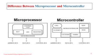
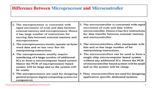
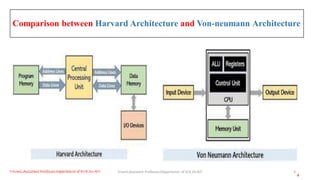
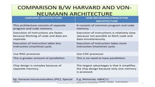
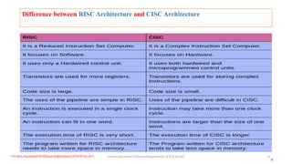
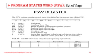
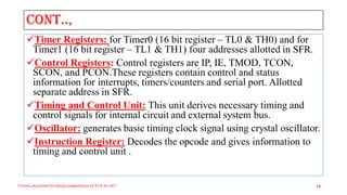
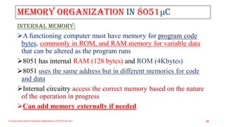
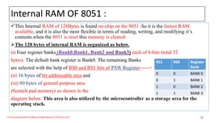
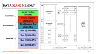
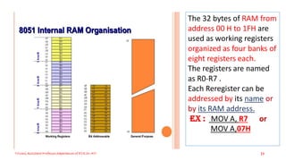
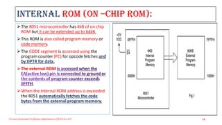
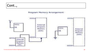
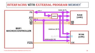
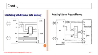
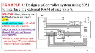
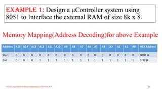
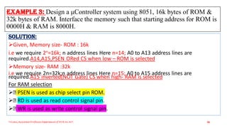
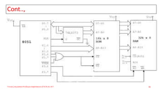
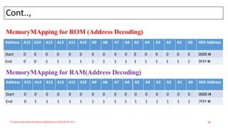
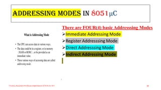
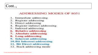
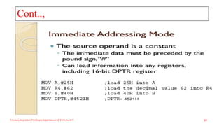
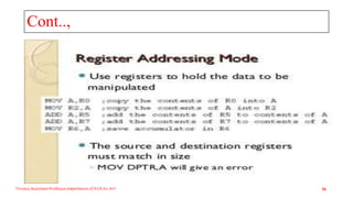
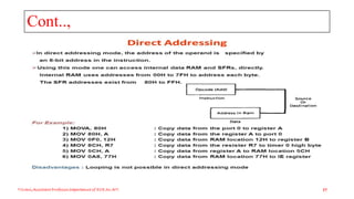
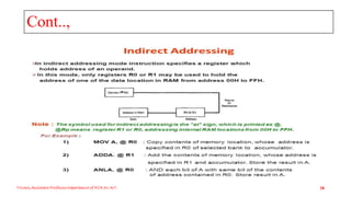
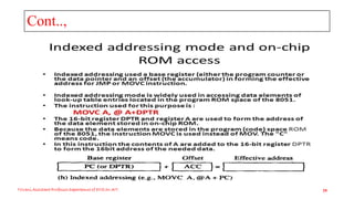
“Microcontrollers and Applications”
8051 Microcontroller
Assistant Professor
ECE Departement
Dr.AIT
1
Triveni,Assistant Professor,Departemnt of ECE,Dr.AIT.
Difference Between Microprocessor and Microcontroller
2
Triveni,Assistant Professor,Departemnt of ECE,Dr.AIT.
Difference Between Microprocessor and Microcontroller
Triveni,Assistant Professor,Departemnt of ECE,Dr.AIT. 3
Triveni,Assistant Professor,Departemnt of ECE,Dr.AIT. 4
Comparison between Harvard Architecture and Von-neumann Architecture
Triveni,Assistant Professor,Departemnt of ECE,Dr.AIT.
4
Triveni,Assistant Professor,Departemnt of ECE,Dr.AIT. 5
Triveni,Assistant Professor,Departemnt of ECE,Dr.AIT. 6
Difference between RISC Architecture and CISC Architecture
Triveni,Assistant Professor,Departemnt of ECE,Dr.AIT.
6
Triveni,Assistant Professor,Departemnt of ECE,Dr.AIT. 7
Brief Histrory
• Intel introduced an 8-bit microcontroller called the 8051.
• It was referred as system on a chip because it had 128 bytes of RAM,
4K byte of on-chip ROM, two timers, one serial port, and 4 ports (8-
bit wide), all on a single chip.
Triveni,Assistant Professor,Departemnt of ECE,Dr.AIT. 8
Block Diagram of 8051 Microcontroller
Triveni,Assistant Professor,Departemnt of ECE,Dr.AIT. 9
Features of 8051 Microcontroller
Triveni,Assistant Professor,Departemnt of ECE,Dr.AIT. 10
4KB bytes on-chip program memory (ROM)
128 bytes on-chip data memory (RAM)
Four register banks
128 user defined software flags
8-bit bidirectional data bus
16-bit unidirectional address bus
32 general purpose registers each of 8-bit
16 bit Timers (usually 2, but may have more or less)
Three internal and two external Interrupts
Four 8-bit ports,(short model have two 8-bit ports)
16-bit program counter and data pointer
 8051 may also have a number of special features such as UARTs, ADC, Op-amp, etc.
Architecture of 8051 Microcontroller
Triveni,Assistant Professor,Departemnt of ECE,Dr.AIT. 11
Accumulator (Acc): Operand register, Implicit or specified in the instruction.it has an address in
on chip SFR bank
B Register:Used to store one of the operands for multiplication and division, otherwise,
scratch pad considered as a SFR.
Stack Pointer (SP): 8 bit wide register. Incremented before data is stored on to the stack using
PUSH or CALL instructions. Stack defined anywhere on the 128 byte RAM.
Data Pointer (DPTR): 16 bit register contains DPH and DPL Pointer to external RAM address.
DPH and DPL allotted separate addresses in SFR bank
Port 0 To 3 Latches & Drivers: Each I/O port allotted a latch and a driver Latches allotted
address in SFR. User can communicate via these ports P0, P1, P2, and P3.
Serial Data Buffer: Internally had TWO independent registers, TRANSMIT buffer (parallel in
serial out – PISO) and RECEIVE buffer (serial in parallel out –SIPO) identified by SBUF and
allotted an address in SFR.
Triveni,Assistant Professor,Departemnt of ECE,Dr.AIT. 12
 Program Status Word (PSW): Set of flags
Triveni,Assistant Professor,Departemnt of ECE,Dr.AIT. 13
Cont..,
Timer Registers: for Timer0 (16 bit register – TL0 & TH0) and for
Timer1 (16 bit register – TL1 & TH1) four addresses allotted in SFR.
Control Registers: Control registers are IP, IE, TMOD, TCON,
SCON, and PCON.These registers contain control and status
information for interrupts, timers/counters and serial port. Allotted
separate address in SFR.
Timing and Control Unit: This unit derives necessary timing and
control signals for internal circuit and external system bus.
Oscillator: generates basic timing clock signal using crystal oscillator.
Instruction Register: Decodes the opcode and gives information to
timing and control unit .
Triveni,Assistant Professor,Departemnt of ECE,Dr.AIT. 14
Cont..,
• EPROM & program address Register: provide on chip EPROM and mechanism to
• address it. All versions don’t have EPROM.
• Ram & Ram Address Register: provide internal 128 bytes RAM and a mechanism to
• address internally
• ALU: Performs 8 bit arithmetic and logical operations over the operands held by TEMP1
• and TEMP 2.User cannot access temporary registers.
• SFR Register Bank: set of special function registers address range: 80 H to FF H.
• Interrupt, serial port and timer units control and perform specific functions under the
• control of timing and control unit.
Triveni,Assistant Professor,Departemnt of ECE,Dr.AIT. 15
8051 pin diagram
Pins 1 to 8 − these pins are known as
Port 1. This port doesn’t serve any
other functions.It is internally pulled
up, bi-directional I/O port.
Pin 9 − It is a RESET pin, which is
used to reset the microcontroller to
its initial values.
Pins 10 to 17 − These pins are known
as Port 3. This port serves some
alternate functions like interrupts,
timer input, control signals, serial
communication signals RxD and TxD,
Triveni,Assistant Professor,Departemnt of ECE,Dr.AIT. 16
PORT 3 PIN FUNCTIONS
Triveni,Assistant Professor,Departemnt of ECE,Dr.AIT. 17
17 16 15 14 13 12 11 10 <--- PIN
NO.,
Cont.,
• Pins 18 & 19 − These pins are used for interfacing an external crystal to get
the system clock.
• Pin 20 − This pin provides the power supply to the circuit.
• Pins 21 to 28 − These pins are known as Port 2. It serves as I/O port. Higher
order address bus signals are also multiplexed using this port.
• Pin 29 − This is PSEN pin which stands for Program Store Enable. It is used
to read a signal from the external program memory.
• Pin 30 − This is EA pin which stands for External Access input. It is used to
enable/disable the external memory interfacing.
• Pin 31 − This is ALE pin which stands for Address Latch Enable. It is used
to demultiplex the address-data signal of port.
• Pins 32 to 39 − These pins are known as Port 0. It serves as I/O port. Lower
order address and data bus signals are multiplexed using this port.
• Pin 40 − This pin is used to provide power supply to the circuit.
Triveni,Assistant Professor,Departemnt of ECE,Dr.AIT. 18
Triveni,Assistant Professor,Departemnt of ECE,Dr.AIT. 19
Triveni,Assistant Professor,Departemnt of ECE,Dr.AIT. 20
INTERNAL MEMORY:
commonly in ROM, and RAM memory for variable data
8051 has internal RAM (128 bytes) and ROM (4Kbytes)
8051 uses the same address but in different memories for code
and data
Internal circuitry access the correct memory based on the nature
of the operation in progress
Can add memory externally if needed
Memory organization in 8051μC
Internal RAM OF 8051 :
This Internal RAM of 128Bytes is found on-chip on the 8051 .So it is the fastest RAM
available, and it is also the most flexible in terms of reading, writing, and modifying it’s
contents.when the 8051 is reset this memory is cleared.
The 128 bytes of internal RAM is organized as below.
(i) Four register banks ) each of 8-bits (total 32
bytes). The default bank register is Bank0. The remaining Banks
are selected with the help of RS0 and RS1 bits of PSW Register------>
(ii) of bit addressable area and
(iii) 80 bytes of general purpose area
(Scratch pad memory) as shown in the
diagram below. This area is also utilized by the microcontroller as a storage area for the
operating stack.
Triveni,Assistant Professor,Departemnt of ECE,Dr.AIT. 21
RS1 RS0 Register
Bank
0 0 BANK 0
0 1 BANK 1
1 0 BANK 2
1 1 BANK 3
Data(RAM) memory
Triveni,Assistant Professor,Departemnt of ECE,Dr.AIT. 22
Triveni,Assistant Professor,Departemnt of ECE,Dr.AIT. 23
The 32 bytes of RAM from
address 00 H to 1FH are
used as working registers
organized as four banks of
eight registers each.
The registers are named
as R0-R7 .
Each Reregister can be
addressed by its name or
by its RAM address.
EX : MOV A, R7 or
MOV A,07H
Internal ROM (On –chip ROM):
The 8051 microcontroller has 4kB of on chip
ROM but it can be extended up to 64kB.
This ROM is also called program memory or
code memory.
The CODE segment is accessed using the
program counter (PC) for opcode fetches and
by DPTR for data.
The external ROM
.
When the Internal ROM address is exceeded
the 8051 automatically fetches the code
bytes from the external program memory.
Triveni,Assistant Professor,Departemnt of ECE,Dr.AIT. 24
Cont..,
Triveni,Assistant Professor,Departemnt of ECE,Dr.AIT. 25
Interfacing with External Program Memory
Triveni,Assistant Professor,Departemnt of ECE,Dr.AIT. 26
Cont..,
Triveni,Assistant Professor,Departemnt of ECE,Dr.AIT. 27
Example 1: Design a μController system using 8051
to Interface the external RAM of size 8k x 8.
Solution: Given, Memory size:
8k Which means, we require
2n=8k:
n address lines Here n=13: A0-12
address lines are required.
A13,A14 and A15 are connected
through OR gate to CS pin of
external RAM.
When A13,A14 and A15 both
are low (logic ‘0’), external data
memory (RAM) is selected.
Triveni,Assistant Professor,Departemnt of ECE,Dr.AIT. 28
Example 1: Design a μController system using
8051 to Interface the external RAM of size 8k x 8.
Triveni,Assistant Professor,Departemnt of ECE,Dr.AIT. 29
Address A15 A14 A13 A12 A11 A10 A9 A8 A7 A6
Start 0 0 0 0 0 0 0 0 0 0
End 0 0 0 1 1 1 1 1 1 1
A5 A4 A3 A2 A1 A0 HEX Address
0 0 0 0 0 0 0000 H
1 1 1 1 1 1 1FFF H
Memory Mapping(Address Decoding)for above Example
Example 3: Design a μController system using 8051, 16k bytes of ROM &
32k bytes of RAM. Interface the memory such that starting address for ROM is
0000H & RAM is 8000H.
Triveni,Assistant Professor,Departemnt of ECE,Dr.AIT. 30
Solution:
Given, Memory size- ROM : 16k
i.e we require 2n=16k; n address lines Here n=14; A0 to A13 address lines are
required.A14,A15,PSEN ORed CS when low – ROM is selected
Memory size- RAM :32k
i.e we require 2n=32k;n address lines Here n=15; A0 to A15 address lines are
required.A15 inverted(NOT Gate) CS when high- RAM is selected
For RAM selection
 PSEN is used as chip select pin ROM.
 RD is used as read control signal pin.
 WR is used as write control signal pin.
Cont..,
Triveni,Assistant Professor,Departemnt of ECE,Dr.AIT. 31
Triveni,Assistant Professor,Departemnt of ECE,Dr.AIT. 32
Address A15 A14 A13 A12 A11 A10 A9 A8 A7 A6
Start 0 0 0 0 0 0 0 0 0 0
End 0 0 1 1 1 1 1 1 1 1
A5 A4 A3 A2 A1 A0 HEX Address
0 0 0 0 0 0 0000 H
1 1 1 1 1 1 3FFF H
Address A15 A14 A13 A12 A11 A10 A9 A8 A7 A6
Start 0 0 0 0 0 0 0 0 0 0
End 0 1 1 1 1 1 1 1 1 1
A5 A4 A3 A2 A1 A0 HEX Address
0 0 0 0 0 0 0000 H
1 1 1 1 1 1 7FFF H
Cont..,
MemoryMApping for ROM (Address Decoding)
MemoryMApping for RAM(Address Decoding)
Addressing Modes in 8051μC
Triveni,Assistant Professor,Departemnt of ECE,Dr.AIT. 33
There are FOUR(4) basic Addresssing Modes
Immediate Addressing Mode
Register Addresssing Mode
Direct Addresssing Mode
Indirect Addressing Mode
Cont..,
Triveni,Assistant Professor,Departemnt of ECE,Dr.AIT. 34
Cont..,
Triveni,Assistant Professor,Departemnt of ECE,Dr.AIT. 35
Cont..,
Triveni,Assistant Professor,Departemnt of ECE,Dr.AIT. 36
Cont..,
Triveni,Assistant Professor,Departemnt of ECE,Dr.AIT. 37
Cont..,
Triveni,Assistant Professor,Departemnt of ECE,Dr.AIT. 38
Cont..,
Triveni,Assistant Professor,Departemnt of ECE,Dr.AIT. 39
Cont..,
Triveni,Assistant Professor,Departemnt of ECE,Dr.AIT. 40
Cont..,
Triveni,Assistant Professor,Departemnt of ECE,Dr.AIT. 41
Cont..,
Triveni,Assistant Professor,Departemnt of ECE,Dr.AIT. 42
Triveni,Assistant Professor,Departemnt of ECE,Dr.AIT. 43

21ECU502_UNIT1.pdf

  • 1.
    “Microcontrollers and Applications” 8051Microcontroller Assistant Professor ECE Departement Dr.AIT 1 Triveni,Assistant Professor,Departemnt of ECE,Dr.AIT.
  • 2.
    Difference Between Microprocessorand Microcontroller 2 Triveni,Assistant Professor,Departemnt of ECE,Dr.AIT.
  • 3.
    Difference Between Microprocessorand Microcontroller Triveni,Assistant Professor,Departemnt of ECE,Dr.AIT. 3
  • 4.
    Triveni,Assistant Professor,Departemnt ofECE,Dr.AIT. 4 Comparison between Harvard Architecture and Von-neumann Architecture Triveni,Assistant Professor,Departemnt of ECE,Dr.AIT. 4
  • 5.
  • 6.
    Triveni,Assistant Professor,Departemnt ofECE,Dr.AIT. 6 Difference between RISC Architecture and CISC Architecture Triveni,Assistant Professor,Departemnt of ECE,Dr.AIT. 6
  • 7.
  • 8.
    Brief Histrory • Intelintroduced an 8-bit microcontroller called the 8051. • It was referred as system on a chip because it had 128 bytes of RAM, 4K byte of on-chip ROM, two timers, one serial port, and 4 ports (8- bit wide), all on a single chip. Triveni,Assistant Professor,Departemnt of ECE,Dr.AIT. 8
  • 9.
    Block Diagram of8051 Microcontroller Triveni,Assistant Professor,Departemnt of ECE,Dr.AIT. 9
  • 10.
    Features of 8051Microcontroller Triveni,Assistant Professor,Departemnt of ECE,Dr.AIT. 10 4KB bytes on-chip program memory (ROM) 128 bytes on-chip data memory (RAM) Four register banks 128 user defined software flags 8-bit bidirectional data bus 16-bit unidirectional address bus 32 general purpose registers each of 8-bit 16 bit Timers (usually 2, but may have more or less) Three internal and two external Interrupts Four 8-bit ports,(short model have two 8-bit ports) 16-bit program counter and data pointer  8051 may also have a number of special features such as UARTs, ADC, Op-amp, etc.
  • 11.
    Architecture of 8051Microcontroller Triveni,Assistant Professor,Departemnt of ECE,Dr.AIT. 11
  • 12.
    Accumulator (Acc): Operandregister, Implicit or specified in the instruction.it has an address in on chip SFR bank B Register:Used to store one of the operands for multiplication and division, otherwise, scratch pad considered as a SFR. Stack Pointer (SP): 8 bit wide register. Incremented before data is stored on to the stack using PUSH or CALL instructions. Stack defined anywhere on the 128 byte RAM. Data Pointer (DPTR): 16 bit register contains DPH and DPL Pointer to external RAM address. DPH and DPL allotted separate addresses in SFR bank Port 0 To 3 Latches & Drivers: Each I/O port allotted a latch and a driver Latches allotted address in SFR. User can communicate via these ports P0, P1, P2, and P3. Serial Data Buffer: Internally had TWO independent registers, TRANSMIT buffer (parallel in serial out – PISO) and RECEIVE buffer (serial in parallel out –SIPO) identified by SBUF and allotted an address in SFR. Triveni,Assistant Professor,Departemnt of ECE,Dr.AIT. 12
  • 13.
     Program StatusWord (PSW): Set of flags Triveni,Assistant Professor,Departemnt of ECE,Dr.AIT. 13
  • 14.
    Cont.., Timer Registers: forTimer0 (16 bit register – TL0 & TH0) and for Timer1 (16 bit register – TL1 & TH1) four addresses allotted in SFR. Control Registers: Control registers are IP, IE, TMOD, TCON, SCON, and PCON.These registers contain control and status information for interrupts, timers/counters and serial port. Allotted separate address in SFR. Timing and Control Unit: This unit derives necessary timing and control signals for internal circuit and external system bus. Oscillator: generates basic timing clock signal using crystal oscillator. Instruction Register: Decodes the opcode and gives information to timing and control unit . Triveni,Assistant Professor,Departemnt of ECE,Dr.AIT. 14
  • 15.
    Cont.., • EPROM &program address Register: provide on chip EPROM and mechanism to • address it. All versions don’t have EPROM. • Ram & Ram Address Register: provide internal 128 bytes RAM and a mechanism to • address internally • ALU: Performs 8 bit arithmetic and logical operations over the operands held by TEMP1 • and TEMP 2.User cannot access temporary registers. • SFR Register Bank: set of special function registers address range: 80 H to FF H. • Interrupt, serial port and timer units control and perform specific functions under the • control of timing and control unit. Triveni,Assistant Professor,Departemnt of ECE,Dr.AIT. 15
  • 16.
    8051 pin diagram Pins1 to 8 − these pins are known as Port 1. This port doesn’t serve any other functions.It is internally pulled up, bi-directional I/O port. Pin 9 − It is a RESET pin, which is used to reset the microcontroller to its initial values. Pins 10 to 17 − These pins are known as Port 3. This port serves some alternate functions like interrupts, timer input, control signals, serial communication signals RxD and TxD, Triveni,Assistant Professor,Departemnt of ECE,Dr.AIT. 16
  • 17.
    PORT 3 PINFUNCTIONS Triveni,Assistant Professor,Departemnt of ECE,Dr.AIT. 17 17 16 15 14 13 12 11 10 <--- PIN NO.,
  • 18.
    Cont., • Pins 18& 19 − These pins are used for interfacing an external crystal to get the system clock. • Pin 20 − This pin provides the power supply to the circuit. • Pins 21 to 28 − These pins are known as Port 2. It serves as I/O port. Higher order address bus signals are also multiplexed using this port. • Pin 29 − This is PSEN pin which stands for Program Store Enable. It is used to read a signal from the external program memory. • Pin 30 − This is EA pin which stands for External Access input. It is used to enable/disable the external memory interfacing. • Pin 31 − This is ALE pin which stands for Address Latch Enable. It is used to demultiplex the address-data signal of port. • Pins 32 to 39 − These pins are known as Port 0. It serves as I/O port. Lower order address and data bus signals are multiplexed using this port. • Pin 40 − This pin is used to provide power supply to the circuit. Triveni,Assistant Professor,Departemnt of ECE,Dr.AIT. 18
  • 19.
  • 20.
    Triveni,Assistant Professor,Departemnt ofECE,Dr.AIT. 20 INTERNAL MEMORY: commonly in ROM, and RAM memory for variable data 8051 has internal RAM (128 bytes) and ROM (4Kbytes) 8051 uses the same address but in different memories for code and data Internal circuitry access the correct memory based on the nature of the operation in progress Can add memory externally if needed Memory organization in 8051μC
  • 21.
    Internal RAM OF8051 : This Internal RAM of 128Bytes is found on-chip on the 8051 .So it is the fastest RAM available, and it is also the most flexible in terms of reading, writing, and modifying it’s contents.when the 8051 is reset this memory is cleared. The 128 bytes of internal RAM is organized as below. (i) Four register banks ) each of 8-bits (total 32 bytes). The default bank register is Bank0. The remaining Banks are selected with the help of RS0 and RS1 bits of PSW Register------> (ii) of bit addressable area and (iii) 80 bytes of general purpose area (Scratch pad memory) as shown in the diagram below. This area is also utilized by the microcontroller as a storage area for the operating stack. Triveni,Assistant Professor,Departemnt of ECE,Dr.AIT. 21 RS1 RS0 Register Bank 0 0 BANK 0 0 1 BANK 1 1 0 BANK 2 1 1 BANK 3
  • 22.
  • 23.
    Triveni,Assistant Professor,Departemnt ofECE,Dr.AIT. 23 The 32 bytes of RAM from address 00 H to 1FH are used as working registers organized as four banks of eight registers each. The registers are named as R0-R7 . Each Reregister can be addressed by its name or by its RAM address. EX : MOV A, R7 or MOV A,07H
  • 24.
    Internal ROM (On–chip ROM): The 8051 microcontroller has 4kB of on chip ROM but it can be extended up to 64kB. This ROM is also called program memory or code memory. The CODE segment is accessed using the program counter (PC) for opcode fetches and by DPTR for data. The external ROM . When the Internal ROM address is exceeded the 8051 automatically fetches the code bytes from the external program memory. Triveni,Assistant Professor,Departemnt of ECE,Dr.AIT. 24
  • 25.
  • 26.
    Interfacing with ExternalProgram Memory Triveni,Assistant Professor,Departemnt of ECE,Dr.AIT. 26
  • 27.
  • 28.
    Example 1: Designa μController system using 8051 to Interface the external RAM of size 8k x 8. Solution: Given, Memory size: 8k Which means, we require 2n=8k: n address lines Here n=13: A0-12 address lines are required. A13,A14 and A15 are connected through OR gate to CS pin of external RAM. When A13,A14 and A15 both are low (logic ‘0’), external data memory (RAM) is selected. Triveni,Assistant Professor,Departemnt of ECE,Dr.AIT. 28
  • 29.
    Example 1: Designa μController system using 8051 to Interface the external RAM of size 8k x 8. Triveni,Assistant Professor,Departemnt of ECE,Dr.AIT. 29 Address A15 A14 A13 A12 A11 A10 A9 A8 A7 A6 Start 0 0 0 0 0 0 0 0 0 0 End 0 0 0 1 1 1 1 1 1 1 A5 A4 A3 A2 A1 A0 HEX Address 0 0 0 0 0 0 0000 H 1 1 1 1 1 1 1FFF H Memory Mapping(Address Decoding)for above Example
  • 30.
    Example 3: Designa μController system using 8051, 16k bytes of ROM & 32k bytes of RAM. Interface the memory such that starting address for ROM is 0000H & RAM is 8000H. Triveni,Assistant Professor,Departemnt of ECE,Dr.AIT. 30 Solution: Given, Memory size- ROM : 16k i.e we require 2n=16k; n address lines Here n=14; A0 to A13 address lines are required.A14,A15,PSEN ORed CS when low – ROM is selected Memory size- RAM :32k i.e we require 2n=32k;n address lines Here n=15; A0 to A15 address lines are required.A15 inverted(NOT Gate) CS when high- RAM is selected For RAM selection  PSEN is used as chip select pin ROM.  RD is used as read control signal pin.  WR is used as write control signal pin.
  • 31.
  • 32.
    Triveni,Assistant Professor,Departemnt ofECE,Dr.AIT. 32 Address A15 A14 A13 A12 A11 A10 A9 A8 A7 A6 Start 0 0 0 0 0 0 0 0 0 0 End 0 0 1 1 1 1 1 1 1 1 A5 A4 A3 A2 A1 A0 HEX Address 0 0 0 0 0 0 0000 H 1 1 1 1 1 1 3FFF H Address A15 A14 A13 A12 A11 A10 A9 A8 A7 A6 Start 0 0 0 0 0 0 0 0 0 0 End 0 1 1 1 1 1 1 1 1 1 A5 A4 A3 A2 A1 A0 HEX Address 0 0 0 0 0 0 0000 H 1 1 1 1 1 1 7FFF H Cont.., MemoryMApping for ROM (Address Decoding) MemoryMApping for RAM(Address Decoding)
  • 33.
    Addressing Modes in8051μC Triveni,Assistant Professor,Departemnt of ECE,Dr.AIT. 33 There are FOUR(4) basic Addresssing Modes Immediate Addressing Mode Register Addresssing Mode Direct Addresssing Mode Indirect Addressing Mode
  • 34.
  • 35.
  • 36.
  • 37.
  • 38.
  • 39.
  • 40.
  • 41.
  • 42.
  • 43.