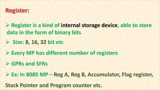
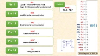
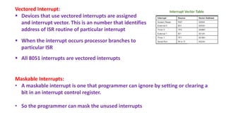
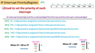
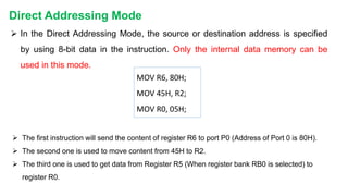
Fundamentals of Microcontroller
8051
Stay Home Stay Safe
By
Dr. Jogade S M
Let us Revise…….  Binary Number
 Bit
 Byte
 Word
 Bus
 Types of Buses
 Register
 IC
 Block Diagram of Computer
 Microprocessor
Binary Number:
Bit: Nibble:
Byte:
Word:
Binary number is a number represented in Base-2 number system,
which consist of only two distinct numbers and
Single binary number or digit Group of binary numbers
Group of binary numbers
Group of binary numbers processed at a time,
it may be of size 4, 8, 16, 32 etc
0 1
4
8
BUS: A Group of conducting lines to carry digital information
Address bus:
Used to carry address of memory and I/O device
and it is unidirectional
Data bus:
Used to carry data and it is bidirectional
Control bus:
Used to carry control signals and it is bidirectional
Types of
Bus
Size of bus is
measured in
terms of Bits
Address Calculation……
Number of
Address bits
Base
21
= 2
Accessing
capacity
22
= 4
23
= 8
24
= 16
25
= 32
26
= 64
28
= 256
29
= 512
27
= 128
2n
= m
n = Number of Address bits (size of address bus)
m = Number of memory locations can be accessed
.
.
.
.
.
211 = 2KB
220
= 1MB
210
= 1024 = 1KB 230
= 1GB
224= 16MB
214 = 16KB 234
= 16GB
212 = 4KB
=
213 8KB
230 = 1GB
220 = 1MB 240 = 1TB
Address calculation continued…….
Finally…….
210 = 1KB
.
.
.
.
.
Register:
 Register is a kind of internal storage device, able to store
data in the form of binary bits
 Size: 8, 16, 32 bit etc
 Every MP has different number of registers
 GPRs and SFRs
 Ex: In 8085 MP – Reg A, Reg B, Accumulator, Flag register,
Stack Pointer and Program counter etc.
Integrated circuit (IC):
Also called as chip, is an entire
electronic circuit consisting of
multiple individual components such as transistors,
diodes, resistors, capacitors and their interconnections
all are fabricated on a single silicon crystal.
Ex: Logic gate ICs (7408), Regulator ICs (7805), IC 555,
Microprocessors (8085), Microcontrollers (8051)
I/P
Devices
O/P
Devices
Block Diagram of computer
Memory
Control Unit
Registers
Arithmetic and Logic Unit
Processor
CPU
(Brain/Heart)
Microprocessor (µP) 8085 Microprocessor
Processor in
the form of IC
is called
Microprocessor
(µP)
Comparison of Microprocessor and Microcontroller
MP consists of ALU, some set of registers, flags, timing and
Control unit
MC contains CPU, Internal RAM, ROM, I/O ports
Timer/counter and interrupts
More number of data transfer instructions Less number of data transfer instructions
Access time for memory and I/O devices is more Access time for memory and I/O devices is less
Cost is high Cost is low
RAM
I//O
ports
µC
CPU
Timers/
counters
Interrupts
ROM
Serial Comm
ports
CPU
ALU
Timing and
Control Unit
Registers
µP
CPU
It cannot be used as standalone It can be used as standalone
Microprocessor based systems are flexible Microcontroller based systems are not flexible
Features of 8051
Microcontroller
Manufacturers
• Introduced by Intel corporation in 1981
• Texas Instruments
• NXP
• Atmel
Package
40 pin
Dual In Line (DIP)
128 bytes
RAM
4KB
ROM
2 Timers
16 bit each
Timers
4 I/O Ports
each of 8 bit
I/O Ports
8 bit
Data Bus
16 bit
Address Bus
6 Interrupts
Interrupts
One
Serial Port
Around
12MHZ
Crystal
Frequency
128 bytes
Can be
extended
upto 64KB
4KB
Can be
extended
upto 64KB
Each timer
is of 16 bits
size
P0 P1 P3
P2
Architecture
of
8051 µC
ALU
CU
Registers
Port 0
Port 3
Port 2
Port 1
Port
P0
P0.0
P0.1
P0.2
P0.4
P0.3
P0.5
P0.6
P0.7
P0, P1, P2, P3
Each of – 8 bits
IO Ports
RST
Logic 1 = Microcontroller is reset
Logic 0 = Microcontroller works normal
Pin 9
RXD
Used for serial communication
Pin 10
TXD
Used for serial communication
Pin 11
INT0’
External interrupt 0
Pin 12
T0
Timer/Counter 0
Pin 14
INT1’
External interrupt 1
Pin 13
Port 1
P1.0 – P1.7
Pin 1 to 8
T1
Timer/Counter 1
Pin 15
WR’
Write Enable
Pin 16
RD’
Read Enable
Pin 17
XTAL2
Provide external clock
Pin 18
XTAL1
Provide external clock
Pin 19
Port 3
P3.0 to P3.7
Pin 10-17
Port 2/ A8-A15
> If the external memory is not used then
these pins are used as I/O port (port 2)
> In case external memory is used the Higher byte
address A8-A15 will appear on these pins
Pin 21 - 28
PSEN’
> Program Store Enable
> Used enable external
ROM memory chip
Pin 29
EA’
> External Access
> EA = Logic 1 = On chip memory accessed
> EA = Logic 0 = External memory accessed
Pin 31
ALE
Used to demultiplex
address and data
Pin 30
Port 0/ A0-A7
> If the external memory is not used then
These pins are used as I/O port (port 0)
> In case external memory is used these pins
are configured as Lower byte address A0-A7 when ALE=1
and Configured as data pins Do-D7 when ALE = 0
Pin 32 - 39
8051 µC
External
ROM
64K
31 EA
29 PSEN
= 0
= 0
PSEN and EA Pins
Memory Organization of 8051 Microcontroller
It provides two memories:
 ROM (Read Only Memory)
 RAM (Random Access Memory)
RAM Memory Organization of 8051µC
RAM/Data
Memory
128 bytes
Decimal Address
0 - 127
Hexadecimal Address
00h - 7Fh
.
.
.
.
0
127
Address in
Decimal
7Fh
00h
Address in
Hexadecimal
RAM
RAM
Memory
128 bytes
7Fh
00h
.
.
.
.
00
07
08
0F
10
17
18
1F
20
2F
30
7F
Bank 0
Bank 2
Bank 1
Bit Addressable RAM
General Purpose Area
(Scratch Pad Memory)
Bank 3
32
bytes
16
bytes
80
bytes
R7
R6
R5
R4
R3
R2
R1
R7
R6
R5
R4
R3
R2
R1
R0
R7
R6
R5
R4
R3
R2
R1
R0
R7
R6
R5
R4
R3
R2
R1
R0
Bank 0 Bank 1
Bank 2 Bank 3
R0
07
03
04
06
05
02
01
00
0F
0B
0C
0E
0D
0A
09
08
1F
1B
1C
1E
1D
1A
19
18
17
13
14
16
15
12
11
10
00 – 1F
Register Bank
Address in
RAM Memory
PSW is a SFR
used to select
‘’Register
Banks”
All bank
registers are
byte
addressable
Bank1- Bank3
locations can
also be used
as Stack
Memory
Register Bank Area in RAM
(32bytes)
Bit Addressable RAM Area
(16 Bytes)
Byte
Address
Bit
Address
General purpose/Scratch Pad RAM Area
(80 Bytes)
On-Chip RAM/ Data Memory Organization in 8051 Microcontroller
Register Banks
32bytes (Reg Banks) + 16bytes (Bit Addressable space) + 80bytes (General Purpose space)
= 128bytes (RAM/Data Memory)
Highlights of RAM Memory Organization…….
 RAM memory is used to store input variables and data types
which are used in the program
ROM/Program
Memory
4 KB
Decimal Address
0 - 4095
Hexadecimal Address
0000h - 0FFFh
.
.
.
.
0
4095
Address in
Decimal
0FFFh
0000h
Address in
Hexadecimal
ROM Memory Organization of 8051µC
ROM
4KB
Internal
ROM
+
60KB
External
ROM
1.
64KB
External
ROM
2.
0000H
0FFFH
1000H
FFFFH
0000H
FFFFH
8051 has
16bit address bus
so
at a time we can use
64KB ROM memory
In both case we need to configure
control pins
ALE, PSEN and EA
 Size of on chip ROM or Program Memory is 4 KB
 Using 16bit address bus 64K of external memory can be accessed
 Either we can use 4K internal ROM plus 60K of external memory or
only external memory of 64K
 Address space of program memory will be 0000H – 0FFFH if only 4K
internal memory is used
 Address space of program memory will be 0000H – FFFFH if 64K memory
is used
Highlights of ROM Memory Organization…….
 ROM memory is used to store the complete program
Special function Registers
00 – 1F: Register Bank Area
20 – 2F: Bit Addressable Area
30 – 7F: General Purpose Area
80 – FF: SFRs
Different Addresses in RAM Memory of 8051
 A Special Function Register (SFR) is a register within a
microcontroller that controls or monitors the various functions
of a microcontroller.
 An SFR can be accessed by its name or by its address.
 A special function register can have an address between 80H to
FFH. As the addresses from 00 to 7FH are the addresses of RAM
memory inside the 8051.
 Not all the address space of 80 to FF are used by the SFR.
Unused locations are reserved and must not be used by the 8051
programmer. Only 21 SFRs are supported by 8051 MC.
Special Function Register (SFR)
It is an 8-bit register
It holds data and receives the result of arithmetic instructions
Can be accessed in several ways
- Implicitly in opcodes (CMA)
- As ACC or A for instructions that allow specifying register (MOV A, R0)
- By its SFR address 0E0H
Bit addressable: to access second bit of accumulator address 0E1H
can be used and for third bit 0E2H and so on
Accumulator (ACC)
Example: MOV A, #09h
 It is an 8-bit register commonly used as temporary register
 Mainly used for multiplication and division
--MUL AB, DIV AB
 B register holds the second operand and part off the result
- Upper 8-bits of the multiplication result
- Remainder in case of division
 Can also be accessed by its SFR address 0F0H
 Bit addressable
Register B
Example: MOV B, #03h
• It can also be used to access RAM memory
 Stack is a section of RAM used to store information temporarily
 Stack Pointer (SP) is 8-bit wide, used to access the stack
 On-Power up or Reset, SP=07H
-24-bytes of RAM memory area - 08H to 1FH
-Register Banks (1,2,3) can be used for stack
 PUSH and POP Instructions
 Stack can be extended: 30H to 7FH
Stack Pointer (SP) (81H)
(99H)
Timer 0 / T0
8A
8C
Timer 1 / T1
8D 8B
0000H
0001H
0002H
.
.
.
.
FFFFH
 8051 has two 16-bit timers (Timer-0 and Timer-1)
 Which can be used either as timer to generate time delay or as counter
to count external events happening outside the microcontroller
Timers
T0 T1
 TF1: Timer 1 overflow flag. Set by hardware when Timer/Counter 1 overflows
 TF0: Timer 0 overflow flag. Set by hardware when Timer/Counter 0 overflows
 TR1: Timer 1 run control bit. Set/cleared by software to turn timer/counter 1 ON/OFF
 TR0: Timer 0 run control bit. Set/cleared by software to turn timer/counter 0 ON/OFF
 IE1: External Interrupt 1(INT1’) flag. When external interrupt occurs, IE1 = 1 otherwise IE1 = 0
 IE0: External Interrupt 0 (INT0’) flag. When external interrupt occurs, IE0 = 1 otherwise IE0 = 0
 IT1: Interrupt 1 type control bit. If IT1 = 1, INT1’ is edge triggering and if IT1 = 0, INT1’ is level triggering
 IT0: Interrupt 0 type control bit. If IT0 = 1, INT0’ is edge triggering and if IT0 = 0, INT0’ is level triggering
(88H) TCON.0
TCON.1
TCON.2
TCON.3
TCON.4
TCON.5
TCON.6
TCON.7
(89H)
TMOD.0
TMOD.1
TMOD.2
TMOD.3
TMOD.4
TMOD.5
TMOD.6
TMOD.7
 8051 has four ports (P0, P1,
P2 and P3) which can be used
as input and/or output port
 Each port has a corresponding
register with same names (i.e.,
P0, P1, P2, P3)
 Each bit in these SFR’s
corresponds to one physical pin
on 8051 IC
 SM0 and SM1: To select different modes of serial port
 SM2: used for multiprocessor communication. Modes 2 and 3 are multiprocessor modes.
To operate Serial modes 2 and 3, this bit should be 1
To operate serial modes 0 and 1, this bit should be 0
 REN: Receiver Enable Bit
When REN=1 then microcontroller can receive serial data from external devices
 TB8: This bit is used in serial mode 2 and 3. It is the 9th bit along with data byte in multiprocessing
When TB8 = 1, byte transmitted is data byte. When TB8 = 0, byte transmitted is address byte
 TI: Transmit Interrupt Flag. When one byte of data transmission is complete through TxD pin, then TI=1
 RI: Receive Interrupt Flag. When one byte of data reception is complete through RxD pin, then RI=1
 RB8: This bit is used in serial mode 2 and 3. It is the 9th bit along with data byte in multiprocessing
When RB8 = 1, byte received is data byte. When RB8 = 0, byte received is address byte
(98H)
PSW (Program Status Word) (D0)
7 6 5 4 3 2 1 0
 As the name indicates, this register is used for efficient power management of 8051 micro
controller. Commonly referred to as PCON register, this is a dedicated SFR for power
management alone.
 From the figure above you can observe that there are 2 modes for this register :-
Idle mode and Power down mode
• During Idle Mode, the Microcontroller will stop the Clock Signal to the ALU (CPU) but it is given
to other peripherals like Timer, Serial, Interrupts, etc.
• In the Power Down Mode, the oscillator will be stopped and the power will be reduced to 2V.
There are two general purpose Flag Bits in the PCON Register, which can be used by the
programmer during execution.
 The SMOD Bit is used to control the Baud Rate of the Serial Port.
PCON (Power Control)
(87H)
Interrupts
Definition: An interrupt is an external or internal event that interrupts the
microcontroller to inform it that a device needs a service
ISR:
• After receiving an interrupt signal, the microcontroller stops current
execution and provides the service to the Interrupted device.
• It provides the service by executing some set of instructions called as
Interrupt Service Routine (ISR) or interrupt handler
• For every interrupt there is a Interrupt Service Routine (ISR) or Interrupt
Handler
• There is a fixed location in memory that holds the address of every ISR
• The group of memory locations to hold the address of ISRs is called
Interrupt Vector Table
Vectored Interrupt:
 Devices that use vectored interrupts are assigned
and interrupt vector. This is an number that identifies
address of ISR routine of particular interrupt
 When the interrupt occurs processor branches to
particular ISR
 All 8051 interrupts are vectored interrupts
Maskable Interrupts:
• A maskable interrupt is one that programmer can ignore by setting or clearing a
bit in an interrupt control register.
• So the programmer can mask the unused interrupts
Interrupt Vector Table
 IP (Interrupt Priority)
 IE (Interrupt Enable)
8051 has 5 Interrupts
Interrupts Priorities
INT0
TF0
INT1
TF1
RI/TI
High
Low
Hardware Interrupts: Interrupt generated due to
External devices through interrupt signal
(INTO and INT1)
Software Interrupts: Interrupt generated due to
program instruction
(TFO, TF1 and RI/TI)
Used to set the priority of each
interrupt
An interrupt having high priority is acknowledged first then low priority interrupt is acknowledged
IE.0
IE.6 IE.3
IE.4
IE.5
IE.7 IE.1
IE.2
IP (Interrupt Priority)Register (B8)
(IP.4) PS = 1 high priority is assigned to serial port interrupt and vice versa
(IP.3) PT1 = 1 high priority is assigned to Timer 1 interrupt and vice versa
(IP.2) PX1 = 1 high priority is assigned to External Interrupt (INT1) interrupt and vice versa
(IP.0) PX0 = 1 high priority is assigned to External Interrupt (INT0) interrupt and vice versa
(IP.1) PT0 = 1 high priority is assigned to Timer 0 interrupt and vice versa
Interrupts
INT0
TF0
INT1
TF1
RI/TI
H
L
When IP = 10H
Interrupts
INT0
TF0
INT1
TF1
RI/TI
H
L
When IP = 00 or FF
 Interrupts can be enabled or disabled by
using this IE register
IE (Interrupt Enable )Register
 EA (IE.7) - It is the global enable bit. When EA=1 all interrupts are enabled,
provided corresponding interrupt enable bit is to be set
When EA=0, all interrupts are disabled
 X (IE.6 and IE.5) – Not used
 ES (IE.4) - When ES=1, Serial port interrupt is enabled and vice versa (provided EA=1).
 ET1 (IE.3) - When ET1=1, Timer 1 interrupt is enabled and vice versa (provided EA=1).
 EX1 (IE.2) - When EX1=1, External Interrupt (INT1) is enabled and vice versa (provided EA=1).
 ET0 (IE.1) - When ET0=1, Timer 0 interrupt is enabled and vice versa (provided EA=1).
 EX0 (IE.0) - When EX0=1, External Interrupt (INT0) is enabled and vice versa (provided EA=1).
IE.0
IE.6 IE.3
IE.4
IE.5
IE.7 IE.1
IE.2
(A8)
Minimum Requirement of 8051 MC
 Power supply
 Reset Circuit
 Clock Circuit
RESET Circuit is connected to Pin 9 of microcontroller to
make microcontroller reset
It is an active high input and normally it is low
The 8051 is reset by holding the RST pin high for at
least two machine cycles and then returning it low
After reset all registers and program counter goes back to
value zero
Reset Circuit
Minimum Requirement of 8051 Microcontroller
 But the content of on-chip RAM is not affected.
VCC
Gnd
5V
8051
There are two method of reset circuit
8051
 Initially RST pin is low
 When power is turned on, capacitor starts
charging and during charging – RST pin goes high
 After some time capacitor becomes fully charged,
when it fully charged it blocks DC current
and RST pin is now directly connected to ground,
so it becomes low again
Power On Reset
Manual Reset
Minimum Requirement of 8051 Microcontroller
Clock Circuit
 All internal operations of the 8051 microcontroller are synchronized by the clock pulses.
These clock pulses are generated by oscillator circuit
 XTAL1 (19) and XTAL2 (18) pins provided by 8051 to connect crystal resonant circuit
as shown in the fig
 Operating frequency range - 1MHz to 12MHz
 8051 has an on-chip oscillator. It needs an external crystal that decides the operating
frequency of the 8051
Machine cycle:
The machine cycle is defined as the smallest interval of time required to
execute any instruction
In 8051 one machine cycle consist of 6 states,
One machine cycle = 6 states
Each state = 2 Oscillator pulses
Instructions may require one, two or four machine cycles to execute any instructions
depending on the type of instructions
Time needed to execute an instruction is calculated as,
T = C x 12
f
Where,
T – Time for instruction to be executed
C – Number of machine cycles
f – Crystal frequency
 In 1981, Intel Corporation introduced an 8-bit microcontroller called the 8051.
 This microcontroller had 128 bytes of RAM, 4K bytes of on-chip ROM, two timers, one serial port, and four ports
(8-bit) all on a single chip.
 Intel's original MCS-51 family was developed using N-type metal-oxide-semiconductor (NMOS) technology like
its predecessor Intel MCS-48, but later versions, identified by a letter C in their name (e.g., 80C51) use
complementary metal–oxide–semiconductor (CMOS) technology and consume less power than their NMOS
predecessors. This made them more suitable for battery-powered devices.
 The 8051 became widely popular after Intel allowed other manufacturers to make any flavor of the 8051 they
please with the condition that they remain code compatible with the 8051.This has led to many versions of the
8051 with different speeds and amount of on-chip ROM marketed by more than half a dozen manufacturers. It is
important to know that although there are different flavors of the 8051, they are all compatible with the original
8051 as far as the instructions are concerned. This means that if you write your program for one, it will run on
any one of them regardless of the manufacturer.
 The major 8051 manufacturers are Intel, Atmel, Dallas Semiconductors, Philips Corporation, Infineon. The
Microcontrollers manufactured by these companies which were based on 8051 architecture are the MCS-51
based microcontrollers.
 The other two members of MCS-51 series were 8052 and 8031 with different features.
Overview and features of MCS-51 Family
Features of 8051 Microcontroller
•4KB bytes on-chip program memory (ROM)
•128 bytes on-chip data memory (RAM)
•Four register banks
•8-bit bidirectional data bus
•16-bit unidirectional address bus
•32 general purpose registers each of 8-bit
•16 bit Timers (usually 2, but may have more or less)
•Three internal and two external Interrupts
•Four 8-bit ports,(short model have two 8-bit ports)
•16-bit program counter and data pointer
Instruction Set of 8051
Opcode Operand
Instruction Format
 Opcode is a operational
code which contains all the
information about the
operation to be performed,
Registers used and memory
location to be accessed
 Operand is data which is to
be operated to perform a
specific task
ADD A, R5
Addressing Mode
The way of specifying data or operand in instruction is called addressing mode
• Immediate Addressing Mode
• Register Addressing Mode
• Direct Addressing Mode
• Register Indirect Addressing Mode
• Indexed Addressing Mode
• Implied Addressing Mode
In 8051 There are six types of addressing modes.
MOV A, #0AFH;
MOV R3, #45H;
MOV DPTR, #FE00H;
Immediate addressing mode
In these instructions, the # symbol is used for immediate data.
In the first instruction, the immediate data is AFH, but one 0 is added at the
beginning. So when the data is starting with A to F, the data should be preceded
by 0.
In the last instruction, there is DPTR. The DPTR stands for Data Pointer. Using this,
it points the external data memory location.
In Immediate Addressing Mode, the data is provided in the instruction itself.
The data is provided immediately after the opcode.
In the register addressing mode the source or destination
data should be present in a register (R0 to R7).
MOV A, R5;
MOV R2, #45H;
MOV R0, A;
Register addressing mode
 In 8051, there is no instruction like MOV R5, R7. But we can get the same result by using this
instruction MOV R5, 07H, or by using MOV 05H, R7.
 But these two instruction will work when the selected register bank is RB0.
 To use another register bank and to get the same effect, we have to add the starting address of
that register bank with the register number. For an example, if the RB2 is selected, and we want to
access R5, then the address will be (10H + 05H = 15H), so the instruction will look like this MOV
15H, R7. Here 10H is the starting address of Register Bank 2.
 In the Direct Addressing Mode, the source or destination address is specified
by using 8-bit data in the instruction. Only the internal data memory can be
used in this mode.
 The first instruction will send the content of register R6 to port P0 (Address of Port 0 is 80H).
 The second one is used to move content from 45H to R2.
 The third one is used to get data from Register R5 (When register bank RB0 is selected) to
register R0.
Direct Addressing Mode
MOV R6, 80H;
MOV 45H, R2;
MOV R0, 05H;
R6
80
7F
81
05
Add
Memory
05
MOV R6, 80H;
Direct Addressing Mode
R2
03
03
MOV 80H, R2;
Direct Addressing Mode
 In this mode, the source or destination address is given in the register (R0, R1, DPTR)
 By using register indirect addressing mode, the internal or external addresses can be accessed.
 The R0 and R1 are used for 8-bit addresses, and DPTR is used for 16-bit addresses, no other registers
can be used for addressing purposes.
Register Indirect Addressing Mode
MOV A, @R0
MOVX A, @DPTR;
ADD A, @R1
MOV@R1, 80H
 In the instructions, the @ symbol is used for register indirect addressing
 In instructions, the X in MOVX indicates the external data memory
 In the first instruction if the R0 is holding 40H, then A will get the content
of internal RAM location 40H
 In the second one, the content of A is overwritten in the location pointed
by DPTR
Register Indirect Addressing Mode
MOV A, @R0
R0
03
80
A
03
Register Indirect Addressing Mode
MOV @R1, 45H
R1
03
80
03
If u want to transfer data from
memory location 45H to memory location 80H
 In the indexed addressing mode, the source memory can only be accessed from
program memory.
 The destination operand is always the register A.
MOVC A, @A+PC;
MOVX A, @DPTR;
 The C in MOVC instruction refers to code memory.
 For the first instruction, let us consider A holds 30H. And the PC value is1125H. The
contents of program memory location 1155H (30H + 1125H) are moved to register A.
Indexed addressing mode
 In the implied addressing mode, there will be a single operand
 These types of instruction can work on specific registers only
 These types of instructions are also known as register specific instruction
RLA;
SWAPA;
 These are 1- byte instruction
 The first one is used to rotate the A register content to the Left
 The second one is used to swap the nibbles in A
Implied Addressing Mode
8051 Microcontroller Instruction Set
• Instruction is a command which is given to the microcontroller to perform
specific task
• Entire group of instructions is called Instruction Set. And a set of instructions
written in a sequence is called program
• Just as our sentences are made of words, a Microcontroller’s program is
made of Instructions. Instructions written in a program tell the Microcontroller
which operation to perform.
• 8051 can have 2 = 256 instructions
8
Types of Instructions in 8051 Microcontroller
Instruction Set
• An Instruction consists of an Opcode followed by Operand(s).
• The Op-Code part of the instruction contains the Mnemonic, which specifies the type of
operation to be performed. All Mnemonics or the Opcode part of the instruction are of
One Byte size.
• Coming to the Operand part of the instruction, it defines the data being processed by
the instructions.
• Operand of size Zero Byte, One Byte or Two Bytes
• The operand can be any of the following:
 No Operand
 Data value
 I/O Port
 Memory Location
 CPU register
MOV R0, #75
ADD A, R5
Opcode Operand
• Based on the operation they perform, all the instructions in the
8051 Microcontroller Instruction Set are divided into five groups.
 Data Transfer Instructions
 Arithmetic Instructions
 Logical Instructions
 Boolean or Bit Manipulation Instructions
 Program Branching Instructions
Data Transfer Instructions
The Data Transfer Instructions are associated with transfer
of data between registers or external program memory or
external data memory. The Mnemonics associated with
Data Transfer are given below.
•MOV
•MOVC
•MOVX
•PUSH
•POP
•XCH
•XCHD
Data Transfer
Instructions
Arithmetic Instructions
Using Arithmetic Instructions, you can perform addition, subtraction,
multiplication and division. The arithmetic instructions also include increment
by one, decrement by one and a special instruction called Decimal Adjust
Accumulator.
The Mnemonics associated with the Arithmetic Instructions of the 8051
Microcontroller Instruction Set are:
• ADD
• ADDC
• SUBB
• INC
• DEC
• MUL
• DIV
• DA A
Also, the operations performed by the arithmetic instructions affect flags like
carry, overflow, zero, etc. in the PSW Register.
Arithmetic
Instructions
Logical Instructions
The next group of instructions are the Logical Instructions, which perform
logical operations like AND, OR, XOR, NOT, Rotate, Clear and Swap.
Logical Instruction are performed on Bytes of data on a bit-by-bit basis.
Mnemonics associated with Logical Instructions are as follows:
•ANL
•ORL
•XRL
•CLR
•CPL
•RL
•RLC
•RR
•RRC
•SWAP
Logical
Instructions
1 0 0 0 0 1 1 0
ACC = 86H
ANL A, #12H
1 0 0 0 0 1 1 0
0 0 0 1 0 0 1 0
0 0 0 0 0 0 1 0
0 0 0 0 0 0 1 0
ACC = 02H
Example:
Result:
1 0 0 0 0 1 1 0
ACC = 86H
ANL A, 55H
1 0 0 0 0 1 1 0
1 0 1 1 0 0 0 1
1 0 0 0 0 0 0 0
1 0 0 0 0 0 0 0
ACC = 80H
Result:
1 0 1 1 0 0 0 1
55 = B1H
Boolean or Bit Manipulation Instructions
As the name suggests, Boolean or Bit Manipulation Instructions will deal with
bit variables. We know that there is a special bit-addressable area in the
RAM and some of the Special Function Registers (SFRs) are also bit
addressable.
The Mnemonics corresponding to the Boolean or Bit Manipulation
instructions are:
• CLR
• SETB
• MOV
• JC
• JNC
• JB
• JNB
• JBC
• ANL
• ORL
• CPL
Boolean
Instructions
Program Branching Instructions
The last group of instructions in the 8051 Microcontroller Instruction Set are the Program
Branching Instructions. These instructions control the flow of program logic. The mnemonics of
the Program Branching Instructions are as follows.
• LJMP
• AJMP
•SJMP
• JZ
• JNZ
• CJNE
• DJNZ
• NOP
• LCALL
• ACALL
• RET
• RETI
• JMP
All these instructions, except the NOP (No Operation) affect the Program Counter (PC) in one
way or other. Some of these instructions has decision making capability before transferring
control to other part of the program.
Branching
Instructions
• An assembly language program is a program written by using assembly
language statements or also called as mnemonics such as MOV, ADD etc., and
directives such as ORG and END.
• Mnemonics tells the microcontroller what to do
• Where as directives ORG and END are used indicate start and end of the
program to the assembler
• Assembler: Is a software which converts source file (assembly language
program) into object file (machine language program)
• An assembly language program consists of for fields: Label, mnemonic,
operands and comment
Assembly Language Programming
1. WAP to to load a byte into memory location 8000H and increment the content of memory location
ORG 0000H
MOV DPTR, #8000H //DPTR = 8000
MOV A, #34H //A = 34H
MOV @DPTR, A //8000 = 34H
INC A //A = 35H
MOV @DPTR, A //8000 = 35H
END
2. WAP to store 01H, 02H, 03H and 04H into registers R1, R2, R3 and R4 of Bank3 and exchange the
contents of R1 and R2
ORG 0000H
SETB PSW.3
SETB PSW.4
MOV R1, #01H
MOV R2, #02H
MOV R3, #03H
MOV R4, #04H
MOV A, R1 //A = 01H
XCH A, R2 //A = 02H and R2 = 01H
MOV R1, A //R1 = 02
END
1. WAP to perform logical AND, OR and complementary operations
MOV A, #67H //8-bit value 67 is loaded into accumulator
MOV R0, #33H // 8-bit value 33 is loaded into R3
ANL A, R0 //logical AND operation with values of Acc and R3
END //end of program
MOV A, #44H
MOV R0, #33H
ORL A, R0
END
MOV A, #22H
MOV R0, #55H
XRL A, R0
END
MOV A, #05H
CPL A
END
Logical Operations
1. WAP to add two 8-bit numbers
ORG 0000H
MOV A, #12H
MOV R0, #34H
ADD A, R0
END
2. WAP to subtract two 8-bit numbers
ORG 0000H
MOV A, #33H
SUBB A, #11H
END
3. WAP to multiply two 8-bit numbers
ORG 0000H
MOV A, #08H
MOV 0F0, #02H
MUL AB
END
4. WAP to divide two 8-bit numbers
ORG 0000H
MOV A, #08H
MOV 0F0, #02H
DIV AB
END
Arithmetic Operations
Jump and Loop
1. WAP to multiply 25 by 10 using the technique of repeated addition and store the
result in R5
ORG 0000H
MOV A, #00H //clear accumulator
MOV R2, #10H //multiplier is placed in R2
AGAIN: ADD A, #25H //add multiplicand to the accumulator
DJNZ R2, AGAIN //repeat until R2 = 0
MOV R5, A //store result in R5
END
2. WAP to add first ten natural numbers
ORG 0000H
MOV A, #00H //clear accumulator
MOV R2, #10H //Load counter value in R2
MOV R0, #00H //Initialize R0 to 0
AGAIN: INC R0 //R0 is incremented by 1 to hold the natural number
ADD A, R0 //add first number to accumulator
DJNZ R2, AGAIN //repeat until R2 = 0 (10 times)
MOV 45H, A //save the result into internal mem loc 45
END
Jump and Loop
WAP to put 55H into the upper RAM locations of 90 – 99H
ORG 0000H
MOV A, #55H //A = 55
MOV R2, #10H //Load counter value in R2
MOV R0, #90H //Initialize R0 with 90
BACK: MOV @R0, A //55 is loaded in mem loc 90 initialised by R0
INC R0
DJNZ R2, BACK //Repeat until R2 becomes 0
END
Jump and Loop
WAP to move the content of 7th bit of Accumulator to pin P0.7 and
also save it in RAM location 08H
ORG 0000H
MOV C, ACC.7
MOV P0.7, C
MOV 08, C
END
Bit manipulation
I/O ports / bit manipulation/delay
WAP to put 55H into the upper RAM locations of 90 – 99H
ORG 0000H
MOV A, #55H //A = 55
MOV R2, #10H //Load counter value in R2
MOV R0, #90H //Initialize R0 with 90
BACK: MOV @R0, A //55 is loaded in mem loc 90 initialised by R0
INC R0
DJNZ R2, BACK //Repeat until R2 becomes 0
END
Fundamentals of Microcontroller 8051 by Dr. Jogade S M, Assistant Professor, Sangameshwar College (Autonomous), Solapur

Fundamentals of Microcontroller 8051 by Dr. Jogade S M, Assistant Professor, Sangameshwar College (Autonomous), Solapur

  • 1.
    Fundamentals of Microcontroller 8051 StayHome Stay Safe By Dr. Jogade S M
  • 2.
    Let us Revise……. Binary Number  Bit  Byte  Word  Bus  Types of Buses  Register  IC  Block Diagram of Computer  Microprocessor
  • 3.
    Binary Number: Bit: Nibble: Byte: Word: Binarynumber is a number represented in Base-2 number system, which consist of only two distinct numbers and Single binary number or digit Group of binary numbers Group of binary numbers Group of binary numbers processed at a time, it may be of size 4, 8, 16, 32 etc 0 1 4 8
  • 4.
    BUS: A Groupof conducting lines to carry digital information Address bus: Used to carry address of memory and I/O device and it is unidirectional Data bus: Used to carry data and it is bidirectional Control bus: Used to carry control signals and it is bidirectional Types of Bus Size of bus is measured in terms of Bits
  • 5.
    Address Calculation…… Number of Addressbits Base 21 = 2 Accessing capacity 22 = 4 23 = 8 24 = 16 25 = 32 26 = 64 28 = 256 29 = 512 27 = 128 2n = m n = Number of Address bits (size of address bus) m = Number of memory locations can be accessed . . . . .
  • 6.
    211 = 2KB 220 =1MB 210 = 1024 = 1KB 230 = 1GB 224= 16MB 214 = 16KB 234 = 16GB 212 = 4KB = 213 8KB 230 = 1GB 220 = 1MB 240 = 1TB Address calculation continued……. Finally……. 210 = 1KB . . . . .
  • 7.
    Register:  Register isa kind of internal storage device, able to store data in the form of binary bits  Size: 8, 16, 32 bit etc  Every MP has different number of registers  GPRs and SFRs  Ex: In 8085 MP – Reg A, Reg B, Accumulator, Flag register, Stack Pointer and Program counter etc.
  • 8.
    Integrated circuit (IC): Alsocalled as chip, is an entire electronic circuit consisting of multiple individual components such as transistors, diodes, resistors, capacitors and their interconnections all are fabricated on a single silicon crystal. Ex: Logic gate ICs (7408), Regulator ICs (7805), IC 555, Microprocessors (8085), Microcontrollers (8051)
  • 9.
    I/P Devices O/P Devices Block Diagram ofcomputer Memory Control Unit Registers Arithmetic and Logic Unit Processor CPU (Brain/Heart)
  • 10.
    Microprocessor (µP) 8085Microprocessor Processor in the form of IC is called Microprocessor (µP)
  • 11.
    Comparison of Microprocessorand Microcontroller MP consists of ALU, some set of registers, flags, timing and Control unit MC contains CPU, Internal RAM, ROM, I/O ports Timer/counter and interrupts More number of data transfer instructions Less number of data transfer instructions Access time for memory and I/O devices is more Access time for memory and I/O devices is less Cost is high Cost is low RAM I//O ports µC CPU Timers/ counters Interrupts ROM Serial Comm ports CPU ALU Timing and Control Unit Registers µP CPU It cannot be used as standalone It can be used as standalone Microprocessor based systems are flexible Microcontroller based systems are not flexible
  • 12.
    Features of 8051 Microcontroller Manufacturers •Introduced by Intel corporation in 1981 • Texas Instruments • NXP • Atmel Package 40 pin Dual In Line (DIP) 128 bytes RAM 4KB ROM 2 Timers 16 bit each Timers 4 I/O Ports each of 8 bit I/O Ports 8 bit Data Bus 16 bit Address Bus 6 Interrupts Interrupts One Serial Port Around 12MHZ Crystal Frequency
  • 13.
    128 bytes Can be extended upto64KB 4KB Can be extended upto 64KB Each timer is of 16 bits size P0 P1 P3 P2 Architecture of 8051 µC ALU CU Registers
  • 14.
    Port 0 Port 3 Port2 Port 1 Port P0 P0.0 P0.1 P0.2 P0.4 P0.3 P0.5 P0.6 P0.7 P0, P1, P2, P3 Each of – 8 bits IO Ports
  • 15.
    RST Logic 1 =Microcontroller is reset Logic 0 = Microcontroller works normal Pin 9 RXD Used for serial communication Pin 10 TXD Used for serial communication Pin 11 INT0’ External interrupt 0 Pin 12 T0 Timer/Counter 0 Pin 14 INT1’ External interrupt 1 Pin 13 Port 1 P1.0 – P1.7 Pin 1 to 8
  • 16.
    T1 Timer/Counter 1 Pin 15 WR’ WriteEnable Pin 16 RD’ Read Enable Pin 17 XTAL2 Provide external clock Pin 18 XTAL1 Provide external clock Pin 19 Port 3 P3.0 to P3.7 Pin 10-17
  • 17.
    Port 2/ A8-A15 >If the external memory is not used then these pins are used as I/O port (port 2) > In case external memory is used the Higher byte address A8-A15 will appear on these pins Pin 21 - 28 PSEN’ > Program Store Enable > Used enable external ROM memory chip Pin 29 EA’ > External Access > EA = Logic 1 = On chip memory accessed > EA = Logic 0 = External memory accessed Pin 31 ALE Used to demultiplex address and data Pin 30 Port 0/ A0-A7 > If the external memory is not used then These pins are used as I/O port (port 0) > In case external memory is used these pins are configured as Lower byte address A0-A7 when ALE=1 and Configured as data pins Do-D7 when ALE = 0 Pin 32 - 39
  • 18.
    8051 µC External ROM 64K 31 EA 29PSEN = 0 = 0 PSEN and EA Pins
  • 20.
    Memory Organization of8051 Microcontroller It provides two memories:  ROM (Read Only Memory)  RAM (Random Access Memory)
  • 21.
    RAM Memory Organizationof 8051µC RAM/Data Memory 128 bytes Decimal Address 0 - 127 Hexadecimal Address 00h - 7Fh . . . . 0 127 Address in Decimal 7Fh 00h Address in Hexadecimal RAM
  • 22.
    RAM Memory 128 bytes 7Fh 00h . . . . 00 07 08 0F 10 17 18 1F 20 2F 30 7F Bank 0 Bank2 Bank 1 Bit Addressable RAM General Purpose Area (Scratch Pad Memory) Bank 3 32 bytes 16 bytes 80 bytes
  • 23.
    R7 R6 R5 R4 R3 R2 R1 R7 R6 R5 R4 R3 R2 R1 R0 R7 R6 R5 R4 R3 R2 R1 R0 R7 R6 R5 R4 R3 R2 R1 R0 Bank 0 Bank1 Bank 2 Bank 3 R0 07 03 04 06 05 02 01 00 0F 0B 0C 0E 0D 0A 09 08 1F 1B 1C 1E 1D 1A 19 18 17 13 14 16 15 12 11 10 00 – 1F Register Bank Address in RAM Memory PSW is a SFR used to select ‘’Register Banks” All bank registers are byte addressable Bank1- Bank3 locations can also be used as Stack Memory Register Bank Area in RAM (32bytes)
  • 24.
    Bit Addressable RAMArea (16 Bytes) Byte Address Bit Address
  • 25.
    General purpose/Scratch PadRAM Area (80 Bytes)
  • 26.
    On-Chip RAM/ DataMemory Organization in 8051 Microcontroller Register Banks 32bytes (Reg Banks) + 16bytes (Bit Addressable space) + 80bytes (General Purpose space) = 128bytes (RAM/Data Memory)
  • 27.
    Highlights of RAMMemory Organization…….  RAM memory is used to store input variables and data types which are used in the program
  • 28.
    ROM/Program Memory 4 KB Decimal Address 0- 4095 Hexadecimal Address 0000h - 0FFFh . . . . 0 4095 Address in Decimal 0FFFh 0000h Address in Hexadecimal ROM Memory Organization of 8051µC ROM
  • 29.
    4KB Internal ROM + 60KB External ROM 1. 64KB External ROM 2. 0000H 0FFFH 1000H FFFFH 0000H FFFFH 8051 has 16bit addressbus so at a time we can use 64KB ROM memory In both case we need to configure control pins ALE, PSEN and EA
  • 30.
     Size ofon chip ROM or Program Memory is 4 KB  Using 16bit address bus 64K of external memory can be accessed  Either we can use 4K internal ROM plus 60K of external memory or only external memory of 64K  Address space of program memory will be 0000H – 0FFFH if only 4K internal memory is used  Address space of program memory will be 0000H – FFFFH if 64K memory is used Highlights of ROM Memory Organization…….  ROM memory is used to store the complete program
  • 31.
  • 32.
    00 – 1F:Register Bank Area 20 – 2F: Bit Addressable Area 30 – 7F: General Purpose Area 80 – FF: SFRs Different Addresses in RAM Memory of 8051
  • 33.
     A SpecialFunction Register (SFR) is a register within a microcontroller that controls or monitors the various functions of a microcontroller.  An SFR can be accessed by its name or by its address.  A special function register can have an address between 80H to FFH. As the addresses from 00 to 7FH are the addresses of RAM memory inside the 8051.  Not all the address space of 80 to FF are used by the SFR. Unused locations are reserved and must not be used by the 8051 programmer. Only 21 SFRs are supported by 8051 MC. Special Function Register (SFR)
  • 37.
    It is an8-bit register It holds data and receives the result of arithmetic instructions Can be accessed in several ways - Implicitly in opcodes (CMA) - As ACC or A for instructions that allow specifying register (MOV A, R0) - By its SFR address 0E0H Bit addressable: to access second bit of accumulator address 0E1H can be used and for third bit 0E2H and so on Accumulator (ACC) Example: MOV A, #09h
  • 38.
     It isan 8-bit register commonly used as temporary register  Mainly used for multiplication and division --MUL AB, DIV AB  B register holds the second operand and part off the result - Upper 8-bits of the multiplication result - Remainder in case of division  Can also be accessed by its SFR address 0F0H  Bit addressable Register B Example: MOV B, #03h
  • 39.
    • It canalso be used to access RAM memory
  • 40.
     Stack isa section of RAM used to store information temporarily  Stack Pointer (SP) is 8-bit wide, used to access the stack  On-Power up or Reset, SP=07H -24-bytes of RAM memory area - 08H to 1FH -Register Banks (1,2,3) can be used for stack  PUSH and POP Instructions  Stack can be extended: 30H to 7FH Stack Pointer (SP) (81H)
  • 41.
  • 42.
    Timer 0 /T0 8A 8C Timer 1 / T1 8D 8B 0000H 0001H 0002H . . . . FFFFH  8051 has two 16-bit timers (Timer-0 and Timer-1)  Which can be used either as timer to generate time delay or as counter to count external events happening outside the microcontroller Timers T0 T1
  • 43.
     TF1: Timer1 overflow flag. Set by hardware when Timer/Counter 1 overflows  TF0: Timer 0 overflow flag. Set by hardware when Timer/Counter 0 overflows  TR1: Timer 1 run control bit. Set/cleared by software to turn timer/counter 1 ON/OFF  TR0: Timer 0 run control bit. Set/cleared by software to turn timer/counter 0 ON/OFF  IE1: External Interrupt 1(INT1’) flag. When external interrupt occurs, IE1 = 1 otherwise IE1 = 0  IE0: External Interrupt 0 (INT0’) flag. When external interrupt occurs, IE0 = 1 otherwise IE0 = 0  IT1: Interrupt 1 type control bit. If IT1 = 1, INT1’ is edge triggering and if IT1 = 0, INT1’ is level triggering  IT0: Interrupt 0 type control bit. If IT0 = 1, INT0’ is edge triggering and if IT0 = 0, INT0’ is level triggering (88H) TCON.0 TCON.1 TCON.2 TCON.3 TCON.4 TCON.5 TCON.6 TCON.7
  • 44.
  • 45.
     8051 hasfour ports (P0, P1, P2 and P3) which can be used as input and/or output port  Each port has a corresponding register with same names (i.e., P0, P1, P2, P3)  Each bit in these SFR’s corresponds to one physical pin on 8051 IC
  • 46.
     SM0 andSM1: To select different modes of serial port  SM2: used for multiprocessor communication. Modes 2 and 3 are multiprocessor modes. To operate Serial modes 2 and 3, this bit should be 1 To operate serial modes 0 and 1, this bit should be 0  REN: Receiver Enable Bit When REN=1 then microcontroller can receive serial data from external devices  TB8: This bit is used in serial mode 2 and 3. It is the 9th bit along with data byte in multiprocessing When TB8 = 1, byte transmitted is data byte. When TB8 = 0, byte transmitted is address byte  TI: Transmit Interrupt Flag. When one byte of data transmission is complete through TxD pin, then TI=1  RI: Receive Interrupt Flag. When one byte of data reception is complete through RxD pin, then RI=1  RB8: This bit is used in serial mode 2 and 3. It is the 9th bit along with data byte in multiprocessing When RB8 = 1, byte received is data byte. When RB8 = 0, byte received is address byte (98H)
  • 47.
    PSW (Program StatusWord) (D0) 7 6 5 4 3 2 1 0
  • 48.
     As thename indicates, this register is used for efficient power management of 8051 micro controller. Commonly referred to as PCON register, this is a dedicated SFR for power management alone.  From the figure above you can observe that there are 2 modes for this register :- Idle mode and Power down mode • During Idle Mode, the Microcontroller will stop the Clock Signal to the ALU (CPU) but it is given to other peripherals like Timer, Serial, Interrupts, etc. • In the Power Down Mode, the oscillator will be stopped and the power will be reduced to 2V. There are two general purpose Flag Bits in the PCON Register, which can be used by the programmer during execution.  The SMOD Bit is used to control the Baud Rate of the Serial Port. PCON (Power Control) (87H)
  • 49.
    Interrupts Definition: An interruptis an external or internal event that interrupts the microcontroller to inform it that a device needs a service ISR: • After receiving an interrupt signal, the microcontroller stops current execution and provides the service to the Interrupted device. • It provides the service by executing some set of instructions called as Interrupt Service Routine (ISR) or interrupt handler • For every interrupt there is a Interrupt Service Routine (ISR) or Interrupt Handler • There is a fixed location in memory that holds the address of every ISR • The group of memory locations to hold the address of ISRs is called Interrupt Vector Table
  • 50.
    Vectored Interrupt:  Devicesthat use vectored interrupts are assigned and interrupt vector. This is an number that identifies address of ISR routine of particular interrupt  When the interrupt occurs processor branches to particular ISR  All 8051 interrupts are vectored interrupts Maskable Interrupts: • A maskable interrupt is one that programmer can ignore by setting or clearing a bit in an interrupt control register. • So the programmer can mask the unused interrupts Interrupt Vector Table
  • 51.
     IP (InterruptPriority)  IE (Interrupt Enable) 8051 has 5 Interrupts Interrupts Priorities INT0 TF0 INT1 TF1 RI/TI High Low Hardware Interrupts: Interrupt generated due to External devices through interrupt signal (INTO and INT1) Software Interrupts: Interrupt generated due to program instruction (TFO, TF1 and RI/TI)
  • 52.
    Used to setthe priority of each interrupt An interrupt having high priority is acknowledged first then low priority interrupt is acknowledged IE.0 IE.6 IE.3 IE.4 IE.5 IE.7 IE.1 IE.2 IP (Interrupt Priority)Register (B8) (IP.4) PS = 1 high priority is assigned to serial port interrupt and vice versa (IP.3) PT1 = 1 high priority is assigned to Timer 1 interrupt and vice versa (IP.2) PX1 = 1 high priority is assigned to External Interrupt (INT1) interrupt and vice versa (IP.0) PX0 = 1 high priority is assigned to External Interrupt (INT0) interrupt and vice versa (IP.1) PT0 = 1 high priority is assigned to Timer 0 interrupt and vice versa Interrupts INT0 TF0 INT1 TF1 RI/TI H L When IP = 10H Interrupts INT0 TF0 INT1 TF1 RI/TI H L When IP = 00 or FF
  • 53.
     Interrupts canbe enabled or disabled by using this IE register IE (Interrupt Enable )Register  EA (IE.7) - It is the global enable bit. When EA=1 all interrupts are enabled, provided corresponding interrupt enable bit is to be set When EA=0, all interrupts are disabled  X (IE.6 and IE.5) – Not used  ES (IE.4) - When ES=1, Serial port interrupt is enabled and vice versa (provided EA=1).  ET1 (IE.3) - When ET1=1, Timer 1 interrupt is enabled and vice versa (provided EA=1).  EX1 (IE.2) - When EX1=1, External Interrupt (INT1) is enabled and vice versa (provided EA=1).  ET0 (IE.1) - When ET0=1, Timer 0 interrupt is enabled and vice versa (provided EA=1).  EX0 (IE.0) - When EX0=1, External Interrupt (INT0) is enabled and vice versa (provided EA=1). IE.0 IE.6 IE.3 IE.4 IE.5 IE.7 IE.1 IE.2 (A8)
  • 54.
    Minimum Requirement of8051 MC  Power supply  Reset Circuit  Clock Circuit
  • 55.
    RESET Circuit isconnected to Pin 9 of microcontroller to make microcontroller reset It is an active high input and normally it is low The 8051 is reset by holding the RST pin high for at least two machine cycles and then returning it low After reset all registers and program counter goes back to value zero Reset Circuit Minimum Requirement of 8051 Microcontroller  But the content of on-chip RAM is not affected.
  • 56.
    VCC Gnd 5V 8051 There are twomethod of reset circuit 8051  Initially RST pin is low  When power is turned on, capacitor starts charging and during charging – RST pin goes high  After some time capacitor becomes fully charged, when it fully charged it blocks DC current and RST pin is now directly connected to ground, so it becomes low again Power On Reset Manual Reset Minimum Requirement of 8051 Microcontroller
  • 57.
    Minimum Requirement of8051 Microcontroller Clock Circuit  All internal operations of the 8051 microcontroller are synchronized by the clock pulses. These clock pulses are generated by oscillator circuit  XTAL1 (19) and XTAL2 (18) pins provided by 8051 to connect crystal resonant circuit as shown in the fig  Operating frequency range - 1MHz to 12MHz  8051 has an on-chip oscillator. It needs an external crystal that decides the operating frequency of the 8051
  • 58.
    Machine cycle: The machinecycle is defined as the smallest interval of time required to execute any instruction In 8051 one machine cycle consist of 6 states, One machine cycle = 6 states Each state = 2 Oscillator pulses Instructions may require one, two or four machine cycles to execute any instructions depending on the type of instructions
  • 59.
    Time needed toexecute an instruction is calculated as, T = C x 12 f Where, T – Time for instruction to be executed C – Number of machine cycles f – Crystal frequency
  • 60.
     In 1981,Intel Corporation introduced an 8-bit microcontroller called the 8051.  This microcontroller had 128 bytes of RAM, 4K bytes of on-chip ROM, two timers, one serial port, and four ports (8-bit) all on a single chip.  Intel's original MCS-51 family was developed using N-type metal-oxide-semiconductor (NMOS) technology like its predecessor Intel MCS-48, but later versions, identified by a letter C in their name (e.g., 80C51) use complementary metal–oxide–semiconductor (CMOS) technology and consume less power than their NMOS predecessors. This made them more suitable for battery-powered devices.  The 8051 became widely popular after Intel allowed other manufacturers to make any flavor of the 8051 they please with the condition that they remain code compatible with the 8051.This has led to many versions of the 8051 with different speeds and amount of on-chip ROM marketed by more than half a dozen manufacturers. It is important to know that although there are different flavors of the 8051, they are all compatible with the original 8051 as far as the instructions are concerned. This means that if you write your program for one, it will run on any one of them regardless of the manufacturer.  The major 8051 manufacturers are Intel, Atmel, Dallas Semiconductors, Philips Corporation, Infineon. The Microcontrollers manufactured by these companies which were based on 8051 architecture are the MCS-51 based microcontrollers.  The other two members of MCS-51 series were 8052 and 8031 with different features. Overview and features of MCS-51 Family
  • 62.
    Features of 8051Microcontroller •4KB bytes on-chip program memory (ROM) •128 bytes on-chip data memory (RAM) •Four register banks •8-bit bidirectional data bus •16-bit unidirectional address bus •32 general purpose registers each of 8-bit •16 bit Timers (usually 2, but may have more or less) •Three internal and two external Interrupts •Four 8-bit ports,(short model have two 8-bit ports) •16-bit program counter and data pointer
  • 63.
  • 64.
    Opcode Operand Instruction Format Opcode is a operational code which contains all the information about the operation to be performed, Registers used and memory location to be accessed  Operand is data which is to be operated to perform a specific task ADD A, R5
  • 65.
    Addressing Mode The wayof specifying data or operand in instruction is called addressing mode • Immediate Addressing Mode • Register Addressing Mode • Direct Addressing Mode • Register Indirect Addressing Mode • Indexed Addressing Mode • Implied Addressing Mode In 8051 There are six types of addressing modes.
  • 66.
    MOV A, #0AFH; MOVR3, #45H; MOV DPTR, #FE00H; Immediate addressing mode In these instructions, the # symbol is used for immediate data. In the first instruction, the immediate data is AFH, but one 0 is added at the beginning. So when the data is starting with A to F, the data should be preceded by 0. In the last instruction, there is DPTR. The DPTR stands for Data Pointer. Using this, it points the external data memory location. In Immediate Addressing Mode, the data is provided in the instruction itself. The data is provided immediately after the opcode.
  • 67.
    In the registeraddressing mode the source or destination data should be present in a register (R0 to R7). MOV A, R5; MOV R2, #45H; MOV R0, A; Register addressing mode  In 8051, there is no instruction like MOV R5, R7. But we can get the same result by using this instruction MOV R5, 07H, or by using MOV 05H, R7.  But these two instruction will work when the selected register bank is RB0.  To use another register bank and to get the same effect, we have to add the starting address of that register bank with the register number. For an example, if the RB2 is selected, and we want to access R5, then the address will be (10H + 05H = 15H), so the instruction will look like this MOV 15H, R7. Here 10H is the starting address of Register Bank 2.
  • 68.
     In theDirect Addressing Mode, the source or destination address is specified by using 8-bit data in the instruction. Only the internal data memory can be used in this mode.  The first instruction will send the content of register R6 to port P0 (Address of Port 0 is 80H).  The second one is used to move content from 45H to R2.  The third one is used to get data from Register R5 (When register bank RB0 is selected) to register R0. Direct Addressing Mode MOV R6, 80H; MOV 45H, R2; MOV R0, 05H;
  • 69.
  • 70.
  • 71.
     In thismode, the source or destination address is given in the register (R0, R1, DPTR)  By using register indirect addressing mode, the internal or external addresses can be accessed.  The R0 and R1 are used for 8-bit addresses, and DPTR is used for 16-bit addresses, no other registers can be used for addressing purposes. Register Indirect Addressing Mode MOV A, @R0 MOVX A, @DPTR; ADD A, @R1 MOV@R1, 80H  In the instructions, the @ symbol is used for register indirect addressing  In instructions, the X in MOVX indicates the external data memory  In the first instruction if the R0 is holding 40H, then A will get the content of internal RAM location 40H  In the second one, the content of A is overwritten in the location pointed by DPTR
  • 72.
    Register Indirect AddressingMode MOV A, @R0 R0 03 80 A 03
  • 73.
    Register Indirect AddressingMode MOV @R1, 45H R1 03 80 03 If u want to transfer data from memory location 45H to memory location 80H
  • 74.
     In theindexed addressing mode, the source memory can only be accessed from program memory.  The destination operand is always the register A. MOVC A, @A+PC; MOVX A, @DPTR;  The C in MOVC instruction refers to code memory.  For the first instruction, let us consider A holds 30H. And the PC value is1125H. The contents of program memory location 1155H (30H + 1125H) are moved to register A. Indexed addressing mode
  • 75.
     In theimplied addressing mode, there will be a single operand  These types of instruction can work on specific registers only  These types of instructions are also known as register specific instruction RLA; SWAPA;  These are 1- byte instruction  The first one is used to rotate the A register content to the Left  The second one is used to swap the nibbles in A Implied Addressing Mode
  • 76.
    8051 Microcontroller InstructionSet • Instruction is a command which is given to the microcontroller to perform specific task • Entire group of instructions is called Instruction Set. And a set of instructions written in a sequence is called program • Just as our sentences are made of words, a Microcontroller’s program is made of Instructions. Instructions written in a program tell the Microcontroller which operation to perform. • 8051 can have 2 = 256 instructions 8
  • 77.
    Types of Instructionsin 8051 Microcontroller Instruction Set • An Instruction consists of an Opcode followed by Operand(s). • The Op-Code part of the instruction contains the Mnemonic, which specifies the type of operation to be performed. All Mnemonics or the Opcode part of the instruction are of One Byte size. • Coming to the Operand part of the instruction, it defines the data being processed by the instructions. • Operand of size Zero Byte, One Byte or Two Bytes • The operand can be any of the following:  No Operand  Data value  I/O Port  Memory Location  CPU register MOV R0, #75 ADD A, R5 Opcode Operand
  • 78.
    • Based onthe operation they perform, all the instructions in the 8051 Microcontroller Instruction Set are divided into five groups.  Data Transfer Instructions  Arithmetic Instructions  Logical Instructions  Boolean or Bit Manipulation Instructions  Program Branching Instructions
  • 79.
    Data Transfer Instructions TheData Transfer Instructions are associated with transfer of data between registers or external program memory or external data memory. The Mnemonics associated with Data Transfer are given below. •MOV •MOVC •MOVX •PUSH •POP •XCH •XCHD
  • 80.
  • 81.
    Arithmetic Instructions Using ArithmeticInstructions, you can perform addition, subtraction, multiplication and division. The arithmetic instructions also include increment by one, decrement by one and a special instruction called Decimal Adjust Accumulator. The Mnemonics associated with the Arithmetic Instructions of the 8051 Microcontroller Instruction Set are: • ADD • ADDC • SUBB • INC • DEC • MUL • DIV • DA A Also, the operations performed by the arithmetic instructions affect flags like carry, overflow, zero, etc. in the PSW Register.
  • 82.
  • 83.
    Logical Instructions The nextgroup of instructions are the Logical Instructions, which perform logical operations like AND, OR, XOR, NOT, Rotate, Clear and Swap. Logical Instruction are performed on Bytes of data on a bit-by-bit basis. Mnemonics associated with Logical Instructions are as follows: •ANL •ORL •XRL •CLR •CPL •RL •RLC •RR •RRC •SWAP
  • 84.
    Logical Instructions 1 0 00 0 1 1 0 ACC = 86H ANL A, #12H 1 0 0 0 0 1 1 0 0 0 0 1 0 0 1 0 0 0 0 0 0 0 1 0 0 0 0 0 0 0 1 0 ACC = 02H Example: Result: 1 0 0 0 0 1 1 0 ACC = 86H ANL A, 55H 1 0 0 0 0 1 1 0 1 0 1 1 0 0 0 1 1 0 0 0 0 0 0 0 1 0 0 0 0 0 0 0 ACC = 80H Result: 1 0 1 1 0 0 0 1 55 = B1H
  • 85.
    Boolean or BitManipulation Instructions As the name suggests, Boolean or Bit Manipulation Instructions will deal with bit variables. We know that there is a special bit-addressable area in the RAM and some of the Special Function Registers (SFRs) are also bit addressable. The Mnemonics corresponding to the Boolean or Bit Manipulation instructions are: • CLR • SETB • MOV • JC • JNC • JB • JNB • JBC • ANL • ORL • CPL
  • 86.
  • 87.
    Program Branching Instructions Thelast group of instructions in the 8051 Microcontroller Instruction Set are the Program Branching Instructions. These instructions control the flow of program logic. The mnemonics of the Program Branching Instructions are as follows. • LJMP • AJMP •SJMP • JZ • JNZ • CJNE • DJNZ • NOP • LCALL • ACALL • RET • RETI • JMP All these instructions, except the NOP (No Operation) affect the Program Counter (PC) in one way or other. Some of these instructions has decision making capability before transferring control to other part of the program.
  • 88.
  • 89.
    • An assemblylanguage program is a program written by using assembly language statements or also called as mnemonics such as MOV, ADD etc., and directives such as ORG and END. • Mnemonics tells the microcontroller what to do • Where as directives ORG and END are used indicate start and end of the program to the assembler • Assembler: Is a software which converts source file (assembly language program) into object file (machine language program) • An assembly language program consists of for fields: Label, mnemonic, operands and comment Assembly Language Programming
  • 90.
    1. WAP toto load a byte into memory location 8000H and increment the content of memory location ORG 0000H MOV DPTR, #8000H //DPTR = 8000 MOV A, #34H //A = 34H MOV @DPTR, A //8000 = 34H INC A //A = 35H MOV @DPTR, A //8000 = 35H END 2. WAP to store 01H, 02H, 03H and 04H into registers R1, R2, R3 and R4 of Bank3 and exchange the contents of R1 and R2 ORG 0000H SETB PSW.3 SETB PSW.4 MOV R1, #01H MOV R2, #02H MOV R3, #03H MOV R4, #04H MOV A, R1 //A = 01H XCH A, R2 //A = 02H and R2 = 01H MOV R1, A //R1 = 02 END
  • 91.
    1. WAP toperform logical AND, OR and complementary operations MOV A, #67H //8-bit value 67 is loaded into accumulator MOV R0, #33H // 8-bit value 33 is loaded into R3 ANL A, R0 //logical AND operation with values of Acc and R3 END //end of program MOV A, #44H MOV R0, #33H ORL A, R0 END MOV A, #22H MOV R0, #55H XRL A, R0 END MOV A, #05H CPL A END Logical Operations
  • 92.
    1. WAP toadd two 8-bit numbers ORG 0000H MOV A, #12H MOV R0, #34H ADD A, R0 END 2. WAP to subtract two 8-bit numbers ORG 0000H MOV A, #33H SUBB A, #11H END 3. WAP to multiply two 8-bit numbers ORG 0000H MOV A, #08H MOV 0F0, #02H MUL AB END 4. WAP to divide two 8-bit numbers ORG 0000H MOV A, #08H MOV 0F0, #02H DIV AB END Arithmetic Operations
  • 93.
    Jump and Loop 1.WAP to multiply 25 by 10 using the technique of repeated addition and store the result in R5 ORG 0000H MOV A, #00H //clear accumulator MOV R2, #10H //multiplier is placed in R2 AGAIN: ADD A, #25H //add multiplicand to the accumulator DJNZ R2, AGAIN //repeat until R2 = 0 MOV R5, A //store result in R5 END
  • 94.
    2. WAP toadd first ten natural numbers ORG 0000H MOV A, #00H //clear accumulator MOV R2, #10H //Load counter value in R2 MOV R0, #00H //Initialize R0 to 0 AGAIN: INC R0 //R0 is incremented by 1 to hold the natural number ADD A, R0 //add first number to accumulator DJNZ R2, AGAIN //repeat until R2 = 0 (10 times) MOV 45H, A //save the result into internal mem loc 45 END Jump and Loop
  • 95.
    WAP to put55H into the upper RAM locations of 90 – 99H ORG 0000H MOV A, #55H //A = 55 MOV R2, #10H //Load counter value in R2 MOV R0, #90H //Initialize R0 with 90 BACK: MOV @R0, A //55 is loaded in mem loc 90 initialised by R0 INC R0 DJNZ R2, BACK //Repeat until R2 becomes 0 END Jump and Loop
  • 96.
    WAP to movethe content of 7th bit of Accumulator to pin P0.7 and also save it in RAM location 08H ORG 0000H MOV C, ACC.7 MOV P0.7, C MOV 08, C END Bit manipulation
  • 97.
    I/O ports /bit manipulation/delay WAP to put 55H into the upper RAM locations of 90 – 99H ORG 0000H MOV A, #55H //A = 55 MOV R2, #10H //Load counter value in R2 MOV R0, #90H //Initialize R0 with 90 BACK: MOV @R0, A //55 is loaded in mem loc 90 initialised by R0 INC R0 DJNZ R2, BACK //Repeat until R2 becomes 0 END