Disadvantages of microprocessor
•The overall system cost is high
• A large sized PCB is required for
assembling all the components
• Overall product design requires more time
• Physical size of the product is big
• A discrete components are used, the
system is not reliable
SJCET
3.
Advantages of Microcontroller
basedSystem
• As the peripherals are integrated into a single chip, the overall
system cost is very less
• The product is of small size compared to micro processor based
system
• The system design now requires very little efforts
• As the peripherals are integrated with a microprocessor the
system is more reliable
• Though microcontroller may have on chip ROM,RAM and I/O
ports, addition ROM, RAM I/O ports may be interfaced
externally if required
• On chip ROM provide a software security
SJCET
4.
Three criteria inChoosing a
Microcontroller
• meeting the computing needs of the task efficiently and
cost effectively
– speed, the amount of ROM and RAM, the number of I/O ports
and timers, size, packaging, power consumption
– easy to upgrade
– cost per unit
– Noise of environment
• availability of software development tools
– assemblers, debuggers, C compilers, emulator, simulator,
technical support
• wide availability and reliable sources of the
microcontrollers
5.
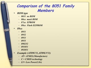
Comparison of the8051 Family
Members
• ROM type
– 8031 no ROM
– 80xx mask ROM
– 87xx EPROM
– 89xx Flash EEPROM
• 89xx
– 8951
– 8952
– 8953
– 8955
– 898252
– 891051
– 892051
• Example (AT89C51,AT89LV51)
– AT= ATMEL(Manufacture)
– C = CMOS technology
– LV= Low Power(3.0v)
6.
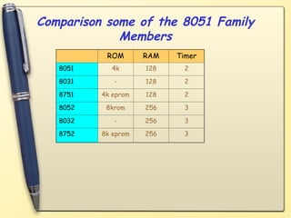
Comparison some ofthe 8051 Family
Members
ROM RAM Timer
8051 4k 128 2
8031 - 128 2
8751 4k eprom 128 2
8052 8krom 256 3
8032 - 256 3
8752 8k eprom 256 3
7.
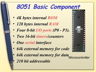
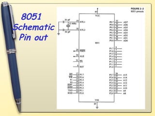
8051 Basic Component
•4K bytes internal ROM
• 128 bytes internal RAM
• Four 8-bit I/O ports (P0 - P3).
• Two 16-bit timers/counters
• One serial interface
• 64k external memory for code
• 64k external memory for data
• 210 bit addressable
Microcontroller
8.
8
The basic 8051Core
• 8-bit CPU optimized for control applications
• Capability for single bit Boolean operations.
• Supports up to 64K of program memory.
• Supports up to 64K of data memory.
• 4 K bytes of on-chip program memory.
• Newer devices provide more.
• 128 or 256 bytes of on-chip data RAM
• Four 8 bit ports.
• Two 16-bit timer/counters
• UART
• Interrupts
• On-chip clock oscillator
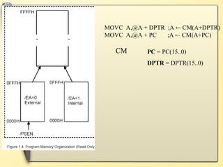
Port 0 withPull-Up Resistors
P0.0
P0.1
P0.2
P0.3
P0.4
P0.5
P0.6
P0.7
DS5000
8751
8951
Vcc
10 K
Port
0
15.
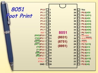
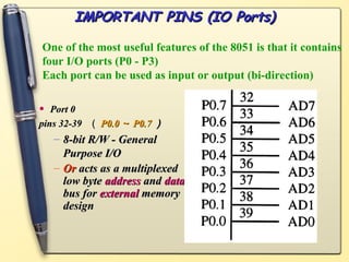
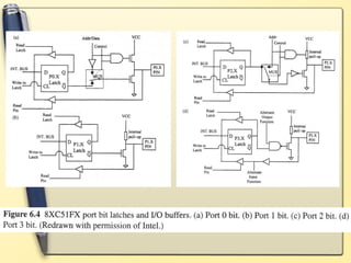
IMPORTANT PINS (IOPorts)
IMPORTANT PINS (IO Ports)
• Port 0
Port 0
pins 32-39
pins 32-39 (
( P0.0
P0.0 ~
~ P0.7
P0.7 )
)
– 8-bit R/W - General
8-bit R/W - General
Purpose I/O
Purpose I/O
– Or
Or acts as a multiplexed
acts as a multiplexed
low byte
low byte address
address and
and data
data
bus for
bus for external
external memory
memory
design
design
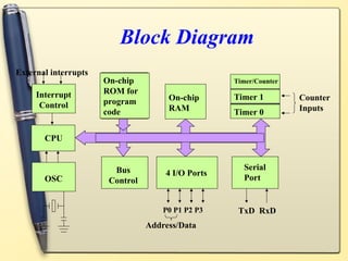
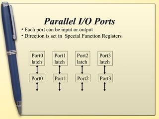
One of the most useful features of the 8051 is that it contains
four I/O ports (P0 - P3)
Each port can be used as input or output (bi-direction)
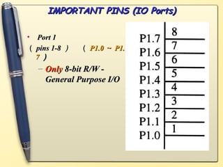
16.
IMPORTANT PINS (IOPorts)
IMPORTANT PINS (IO Ports)
• Port 1
Port 1
(
( pins 1-8
pins 1-8 )
) (
( P1.0
P1.0 ~
~ P1.
P1.
7
7 )
)
– Only
Only 8-bit R/W -
8-bit R/W -
General Purpose I/O
General Purpose I/O
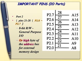
17.
IMPORTANT PINS (IOPorts)
IMPORTANT PINS (IO Ports)
• Port 2
Port 2
• (
( pins 21-28
pins 21-28 (
( P2.0
P2.0 ~
~
P2.7
P2.7 )
)
– 8-bit R/W -
8-bit R/W -
General Purpose
General Purpose
I/O
I/O
– Or
Or high
high byte of
byte of
the
the address
address bus
bus
for external
for external
memory design
memory design
18.
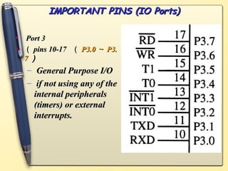
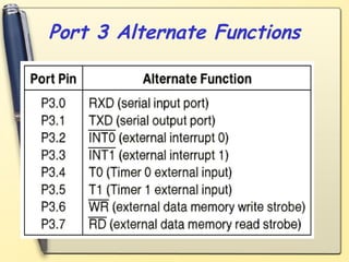
IMPORTANT PINS (IOPorts)
IMPORTANT PINS (IO Ports)
• Port 3
Port 3
• (
( pins 10-17
pins 10-17 (
( P3.0
P3.0 ~
~ P3.
P3.
7
7 )
)
– General Purpose I/O
General Purpose I/O
– if not using any of the
if not using any of the
internal peripherals
internal peripherals
(timers) or external
(timers) or external
interrupts.
interrupts.
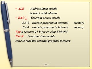
• ALE -Address latch enable
to select valid address
• EA/Vpp - External access enable
EA-0 execute program in external memory
EA-1 execute program in internal memory
Vpp it receives 21 V for on chip EPROM
PSEN Program store enable
store to read the external program memory
SJCET
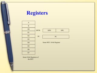
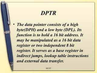
DPTR
• The datapointer consists of a high
byte(DPH) and a low byte (DPL). Its
function is to hold a 16 bit address. It
may be manipulated as a 16 bit data
register or two independent 8 bit
register. It serves as a base register in
indirect jumps, lookup table instructions
and external data transfer.
SJCET
25.
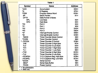
PROGRAM STATUS WORD(PSW)
CY AC F0 RS1 RS0 OV P
SJCET
RS0 RS1 BANK SELECTION
0 0 00H – 07H BANK0
0 1 08H – 0FH BANK 1
1 0 10H – 17H BANK2
1 1 18H – 1FH BANK 3
26.
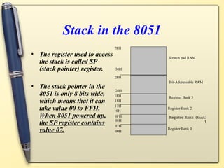
Stack in the8051
• The register used to access
the stack is called SP
(stack pointer) register.
• The stack pointer in the
8051 is only 8 bits wide,
which means that it can
take value 00 to FFH.
When 8051 powered up,
the SP register contains
value 07.
7FH
30H
2FH
20H
1FH
17H
10H
0FH
07H
08H
18H
00H
Register Bank 0
(
Stack
)
Register Bank
1
Register Bank 2
Register Bank 3
Bit-Addressable RAM
Scratch pad RAM
27.
Memory Organization
• The8051 memory organization is rather complex.
• The 8051 has separate address spaces for Program Memory, Data Memory, and
external RAM.
• This is refereed to as a Harvard architecture.
– The early Mark I (1944) computer developed at Harvard was of this type of
architecture.
– Von Neumann at Princeton pointed out that it was not necessary to put
instructions and data in separate memories.
– Most machines have been Princeton architecture.
– Recently Harvard architecture has been employed to help alleviate the
memory bottleneck.
• Both program memory and external data memory are 8 bits wide and use 16 bits
of address. The internal data memory is accessed using an 8-bit address.
• Since the same address can refer to different locations the specific location is
determined by the type of instruction.
28.
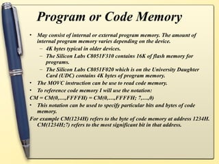
Program or CodeMemory
• May consist of internal or external program memory. The amount of
internal program memory varies depending on the device.
– 4K bytes typical in older devices.
– The Silicon Labs C8051F310 contains 16K of flash memory for
programs.
– The Silicon Labs C8051F020 which is on the University Daughter
Card (UDC) contains 4K bytes of program memory.
• The MOVC instruction can be use to read code memory.
• To reference code memory I will use the notation:
CM = CM(0,…,FFFFH) = CM(0,…,FFFFH; 7,…,0)
• This notation can be used to specify particular bits and bytes of code
memory.
For example CM(1234H) refers to the byte of code memory at address 1234H.
CM(1234H;7) refers to the most significant bit in that address.
29.
CM
MOVC A,@A +DPTR ;A CM(A+DPTR)
MOVC A,@A + PC ;A CM(A+PC)
PC = PC(15..0)
DPTR = DPTR(15..0)
30.
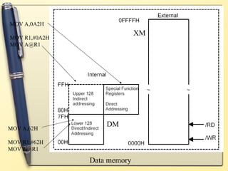
External Memory
• Supportsup to 64K bytes external memory.
– XM(0000,…,FFFF)
= XM(0000,…,FFFF; 7,…,0)
– Accessed by using the MOVX instruction.
• On the original using external memory reduces
number of available I/O ports.
• On some new devices this is not the case.
– For example in C8051F020 64K bytes of external memory
has been included in the chip.
– The 4 standard 8051 ports are available and three
additional ports have been added.
MOVX A,@DPTR ;A XM(DPTR)
MOVX A,@Rn ;A XM(P2|Rn)
MOVX @DPTR,A ;XM(DPTR) A
MOVX @Rn,A ;XM(P2|Rn) A
31.
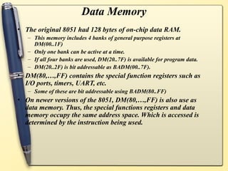
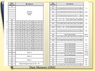
Data Memory
• Theoriginal 8051 had 128 bytes of on-chip data RAM.
– This memory includes 4 banks of general purpose registers at
DM(00..1F)
– Only one bank can be active at a time.
– If all four banks are used, DM(20..7F) is available for program data.
– DM(20..2F) is bit addressable as BADM(00..7F).
• DM(80,…,FF) contains the special function registers such as
I/O ports, timers, UART, etc.
– Some of these are bit addressable using BADM(80..FF)
• On newer versions of the 8051, DM(80,…,FF) is also use as
data memory. Thus, the special functions registers and data
memory occupy the same address space. Which is accessed is
determined by the instruction being used.
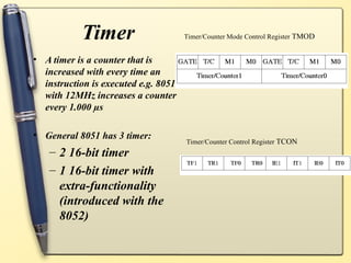
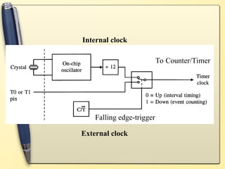
Timer
• A timeris a counter that is
increased with every time an
instruction is executed e.g. 8051
with 12MHz increases a counter
every 1.000 µs
• General 8051 has 3 timer:
– 2 16-bit timer
– 1 16-bit timer with
extra-functionality
(introduced with the
8052)
Timer/Counter Mode Control Register TMOD
Timer/Counter Control Register TCON
37.
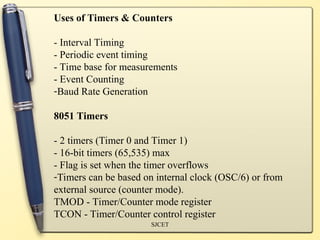
SJCET
Uses of Timers& Counters
- Interval Timing
- Periodic event timing
- Time base for measurements
- Event Counting
-Baud Rate Generation
8051 Timers
- 2 timers (Timer 0 and Timer 1)
- 16-bit timers (65,535) max
- Flag is set when the timer overflows
-Timers can be based on internal clock (OSC/6) or from
external source (counter mode).
TMOD - Timer/Counter mode register
TCON - Timer/Counter control register
38.
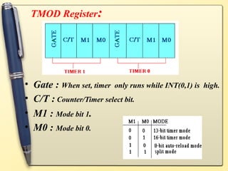
TMOD Register:
• Gate: When set, timer only runs while INT(0,1) is high.
• C/T : Counter/Timer select bit.
• M1 : Mode bit 1.
• M0 : Mode bit 0.
39.
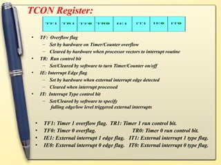
TCON Register:
• TF1:Timer 1 overflow flag. TR1: Timer 1 run control bit.
• TF0: Timer 0 overflag. TR0: Timer 0 run control bit.
• IE1: External interrupt 1 edge flag. IT1: External interrupt 1 type flag.
• IE0: External interrupt 0 edge flag. IT0: External interrupt 0 type flag.
• TF: Overflow flag
– Set by hardware on Timer/Counter overflow
– Cleared by hardware when processor vectors to interrupt routine
• TR: Run control bit
– Set/Cleared by software to turn Timer/Counter on/off
• IE: Interrupt Edge flag
– Set by hardware when external interrupt edge detected
– Cleared when interrupt processed
• IT: Interrupt Type control bit
– Set/Cleared by software to specify
falling edge/low level triggered external interrupts
SJCET
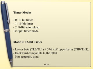
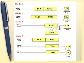
Timer Modes
- 0:13 bit timer
- 1: 16-bit timer
- 2: 8-Bit auto reload
-3: Split timer mode
Mode 0: 13-Bit Timer
- Lower byte (TL0/TL1) + 5 bits of upper bytes (TH0/TH1).
- Backward compatible to the 8048
- Not generally used
42.
SJCET
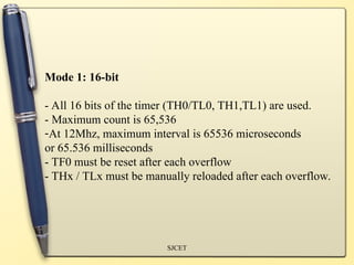
Mode 1: 16-bit
-All 16 bits of the timer (TH0/TL0, TH1,TL1) are used.
- Maximum count is 65,536
-At 12Mhz, maximum interval is 65536 microseconds
or 65.536 milliseconds
- TF0 must be reset after each overflow
- THx / TLx must be manually reloaded after each overflow.
43.
SJCET
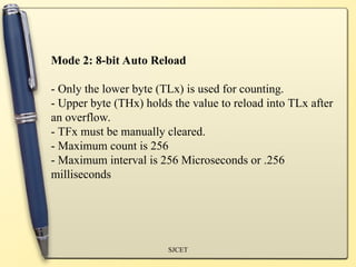
Mode 2: 8-bitAuto Reload
- Only the lower byte (TLx) is used for counting.
- Upper byte (THx) holds the value to reload into TLx after
an overflow.
- TFx must be manually cleared.
- Maximum count is 256
- Maximum interval is 256 Microseconds or .256
milliseconds
44.
SJCET
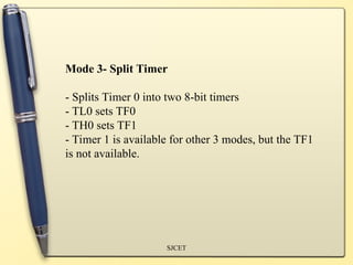
Mode 3- SplitTimer
- Splits Timer 0 into two 8-bit timers
- TL0 sets TF0
- TH0 sets TF1
- Timer 1 is available for other 3 modes, but the TF1
is not available.
SJCET
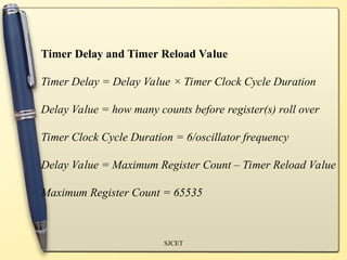
Timer Delay andTimer Reload Value
Timer Delay = Delay Value × Timer Clock Cycle Duration
Delay Value = how many counts before register(s) roll over
Timer Clock Cycle Duration = 6/oscillator frequency
Delay Value = Maximum Register Count – Timer Reload Value
Maximum Register Count = 65535