The document provides an overview of the Intel 8051 microcontroller, including:
- Its internal architecture which includes CPU, RAM, ROM, registers, timers, serial port, and I/O ports.
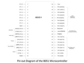
- Pin descriptions and functions for the 40-pin chip.
- Memory organization and interfacing with external memory.
- Clock generation using an external crystal oscillator.
- Features like timers, interrupts, and serial communication.


![The DPL and DPH Registers
• Two 8-bit registers that can be combined into a 16-bit DPTR – Data
Pointer.
• Used by commands that access external memory
• Also used for storing 16bit values
mov DPTR, #data16
; setup DPTR with 16bit ext address
movx A, @DPTR
; copy mem[DPTR] to A
• Can be accessed as 2 separate 8-bit registers if needed.
• DPTR is useful for string operations and Look-Up-Table (LUT)
operations.](https://image.slidesharecdn.com/mpmcunitiv-210531100531/85/8051-Microcontroller-28-320.jpg)


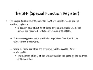
![Data Storage
• The 8051 has 256 bytes of RAM on-chip.
– The lower 128 bytes are intended for internal data storage.
– The upper 128 bytes are the Special Function Registers
(SFR).
• The lower 128 bytes are not to be used as standard RAM.
– Internally 8051’s registers default to stack area, and other
features. [00-7FH]
Link: Memory Organization](https://image.slidesharecdn.com/mpmcunitiv-210531100531/85/8051-Microcontroller-42-320.jpg)
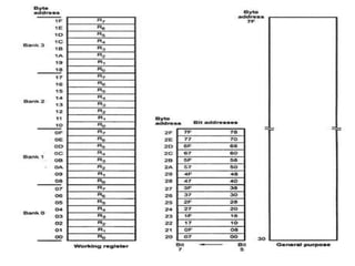
![Data Storage [Cont...]
• The lowest 32 bytes of the on-chip RAM form 4 banks of 8
registers each.
• Only one of these banks can be active at any time.
• Bank is chosen by setting 2 bits in PSW
– Default bank (at power up) is bank 0 (locations 00 – 07).
• The 8 registers in any active bank are referred to as R0 through
R7
• Given that each register has a specific address, it can be
accessed directly using that address even if its bank is not the
active one.](https://image.slidesharecdn.com/mpmcunitiv-210531100531/85/8051-Microcontroller-43-320.jpg)
![Data Storage [Cont...]
• The next 16 bytes – locations 20H to 2FH – form a block that
can be addressed as either bytes or individual bits.
– The bytes have addresses 20H to 2FH.
– The bits have addresses 00H to 7FH.
– Specific instructions are used for accessing
the bits.
• Locations 30H to 7FH are general purpose RAM.
Link: Memory Organization](https://image.slidesharecdn.com/mpmcunitiv-210531100531/85/8051-Microcontroller-44-320.jpg)
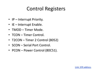
![The Elements of SFR
• ACC and B registers – 8 bit each
• DPTR : [DPH:DPL] – 16 bit combined
• PC (Program Counter) – 16 bits
• SP (Stack Pointer) – 8 bit
• PSW (Program Status Word)
• Port Latches
• Serial Data Buffer
• Timer Registers
• Control Registers
Link: SFR Elements](https://image.slidesharecdn.com/mpmcunitiv-210531100531/85/8051-Microcontroller-46-320.jpg)


![Microcontroller Intel 8051
[Instruction Set]](https://image.slidesharecdn.com/mpmcunitiv-210531100531/85/8051-Microcontroller-62-320.jpg)
![Structure of Assembly Language
[ label: ] mnemonic [operands] [ ;comment ]
Example:
MOV R1, #25H ; load data 25H into R1
63](https://image.slidesharecdn.com/mpmcunitiv-210531100531/85/8051-Microcontroller-63-320.jpg)


![ADDA, Source ;A=A+SOURCE
ADDA,#6 ;A=A+6
ADDA,R6 ;A=A+R6
ADD A,6 ;A=A+[6] or A=A+R6
ADD A,0F3H ;A=A+[0F3H]
SUBB A, Source ;A=A-SOURCE-C
SUBB A,#6 ;A=A-6
SUBB A,R6 ;A=A+R6](https://image.slidesharecdn.com/mpmcunitiv-210531100531/85/8051-Microcontroller-91-320.jpg)


![DEC byte ;byte=byte-1
INC byte ;byte=byte+1
INC R7
DEC A
DEC 40H ; [40]=[40]-1](https://image.slidesharecdn.com/mpmcunitiv-210531100531/85/8051-Microcontroller-94-320.jpg)


![ADD TWO 8 BIT NUMBERS
MOV DPTR, #2400
MOVX A,@DPTR INPUTS:
MOV R1,A [2400]: 08
INC DPTR [2401]:07
MOVX A,@DPTR OUTPUTS: [2402]:0F
MOV R0,#00 [2403]:00
ADD A,R1 AA+R1
JNC L1
INC RO
L1: INC DPTR
MOVX @DPTR,A
INC DPTR
MOV A,RO
MOVX @DPTR,A
L2:SJMP:L2](https://image.slidesharecdn.com/mpmcunitiv-210531100531/85/8051-Microcontroller-106-320.jpg)
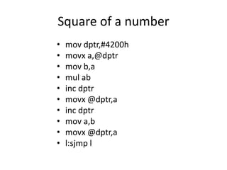
![Multiplication of two numbers
MOV DPTR,#2400
MOVX A,@DPTR
MOV B,A
INC DPTR [2401]
MOVX A,@DPTR
MUL AB
INC DPTR [2402]
MOVX @DPTR,A
INC DPTR [2403]
MOV A,B
MOVX @DPTR,A
L1:SJMP:L1](https://image.slidesharecdn.com/mpmcunitiv-210531100531/85/8051-Microcontroller-107-320.jpg)