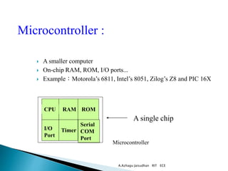
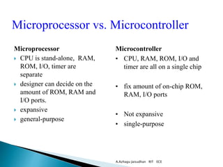
The document provides an overview of the 8051 microcontroller, including its basic architecture and components. It describes the CPU, memory organization, registers, I/O ports, timers and interrupts. Diagrams show the pin connections for external memory and crystal oscillator. Key aspects covered include the 8051 having 4K of on-chip ROM, 128 bytes of RAM, four 8-bit I/O ports, two 16-bit timers, and support for external memory, interrupts and serial communication. Designers need to understand both the programmer and hardware views of microcontrollers.
The document provides an introduction to embedded systems, describing their basic components including hardware, software, and additional electrical and mechanical parts combined on a single microcontroller chip. It then discusses specific microcontrollers like the 8051 and 8085, outlining their architecture, programming, and common applications in devices like digital clocks and traffic lights. Pinouts and programming of timers, interrupts, and I/O are described for the 8051 and 8085 microcontrollers.
The document describes the Intel 8086 microprocessor, which was launched in 1978 as the first 16-bit microprocessor. It had major improvements over the 8085 microprocessor, with higher execution speeds. The 8086 had a 16-bit data bus, 20-bit address bus, and could address up to 1MB of memory. It included features like multiplication and division support. The document provides detailed information on the various pins and signals of the 8086 microprocessor.
The document discusses the 8051 microcontroller. It describes the basic components of the 8051 including 4K bytes of internal ROM, 128 bytes of internal RAM, four 8-bit I/O ports, two 16-bit timers/counters, and one serial interface. It also provides details on the block diagram, important pins like ports and serial interface pins, and how to connect an external clock source to the 8051.
The document discusses various aspects of 8051 assembly language programming including:
- The most commonly used 8-bit registers in the 8051 and the 16-bit program counter and data pointer registers.
- Examples of MOV and ADD instructions to move data between registers and perform arithmetic operations in the accumulator register.
- The steps required to assemble and run an 8051 program, including creating an assembly source file, assembling it to produce object and list files, and optionally linking files to run on a simulator.
- Memory allocation and usage in the 8051 including the 64KB program memory space accessed by the 16-bit program counter and RAM allocation for registers and stack.
The document discusses the 8051 microcontroller, including its architecture, pin configuration, memory organization, timers, interrupts, and interfacing capabilities. It describes the 8051's features like on-chip RAM, ROM, timers and low power consumption which make it suitable for control applications. The document outlines the differences between microprocessors and microcontrollers, and covers various interfacing examples like switches, LEDs, 7-segment displays, LCDs, ADCs and relay interfacing. It concludes with common applications of the 8051 such as in automobiles, industrial processing, robotics and consumer electronics.
Microprocessors are computer components made from transistors on a single chip that serve as the central processing unit (CPU) of computers. Microcontrollers are specialized microprocessors designed to control electronic devices. The key differences are that microcontrollers incorporate additional features like RAM, ROM, I/O ports directly on the chip to be self-sufficient, whereas microprocessors rely on external components. An 80286 microprocessor has features like a 16-bit data bus, 24-bit address bus, and memory management abilities. It was used in early PCs and can address up to 16MB of RAM. Microcontrollers are commonly found in embedded systems like appliances and control specific tasks without changes throughout their lifetime.
The document describes the 8051 microcontroller, its features which include 4 I/O ports, 2 timers, serial communication interface, and interrupts. It discusses the internal architecture such as memory organization, registers, and oscillator circuit. The document also provides details on the ports, timers, serial communication, and power modes of the 8051 microcontroller.
This document discusses JK flip-flops and their applications in counters and seven segment displays. It describes the structure of a JK flip-flop, including its inputs of J, K, PR, CLR and CLK, and its outputs of Q and Q'. It explains the four modes of operation for a JK flip-flop: hold, set, reset, and toggle. Counters are described as using multiple flip-flops connected in series to count pulses. Seven segment displays are discussed as a way to display numbers visually using an arrangement of LED segments, with drivers needed to interpret BCD input for the display.
This document provides an introduction to pins, ports, and configuring pins on the ARM LPC2148 microcontroller. It discusses pin configuration, the different ports on the LPC2148, and how to configure pins as inputs, outputs, or alternate functions using the various IO registers. It also provides an example program for blinking an LED connected to pin P1.16 to demonstrate basic pin configuration and output. The document concludes with an assignment to draw the LED blinking circuit and modify the program to blink LEDs on pins P0.16 through P0.23.
This document provides an overview of assembly language programming for the 8085 microprocessor. It discusses the 8085 programming model including registers, flags, and addressing modes. The document also covers the instruction set categories such as data transfer, arithmetic, logical and branching instructions. Examples are given to demonstrate how to write an assembly language program for the 8085 including analyzing a problem, developing an algorithm, flowchart, and coding the solution. Input/output and memory addressing modes are also explained.
The document provides information about the Intel 8085 microprocessor. Some key details include:
- It is an 8-bit processor that operates on a 5V power supply with a maximum clock frequency of 3MHz.
- It has 40 pins and uses a multiplexed address/data bus. It can access 64KB of memory space and 256 I/O ports.
- It has one accumulator, flag, and six general purpose registers. It supports various addressing modes and 74 instructions.
- Interrupts include TRAP, RST 5.5, RST 6.5, RST 7.5, and INTR. Serial I/O is also supported directly.
-
The document is a seminar report on FPGA technology in outer space applications. It discusses the history and evolution of FPGA technology over time, including increasing gate densities and falling prices. It describes typical FPGA architecture which includes configurable logic blocks, interconnects, and I/O pads. Modern FPGAs integrate additional resources like memory blocks, DSP slices, and soft processor cores. The document highlights applications of FPGAs in aerospace, including COTS boards and development kits. It also outlines future potential for FPGAs in more complex roles in space systems.
The Atmega328 is a low-power 8-bit microcontroller based on AVR architecture that can achieve throughputs of 1 MIPS per MHz. It has 32KB of flash memory, 1KB of EEPROM, 2KB of SRAM, 3 I/O ports, 32 general purpose registers, and a 16-bit timer/counter that can generate delays of up to 262ms when running on a 16MHz oscillator.
The instruction set of the 8085 microprocessor contains 246 instructions that are classified into different types such as data transfer, arithmetic, logical, branching, and control instructions. Data transfer instructions move data between registers and memory locations. Arithmetic instructions perform operations like addition, subtraction, increment, and decrement. Logical instructions perform logical operations like AND, OR, XOR on registers and memory.
The document provides an overview of microcontrollers and the 8051 microcontroller. It begins with a brief history of microcontrollers and how they evolved from microprocessors by integrating RAM, ROM, I/O and other components onto a single chip. It then describes the architecture and components of the 8051 microcontroller, including its memory mapping, registers, I/O ports, timers and interrupts. Examples are given of how the 8051's timers and I/O ports can be programmed. The document aims to educate designers on the capabilities and programming of the 8051 microcontroller.
This document describes the features and specifications of the ATmega32 8-bit microcontroller. It includes details on the microcontroller's architecture such as its AVR CPU core, 32K bytes of flash memory, 1024 bytes of EEPROM, 2K bytes of SRAM, and various peripherals. It also provides information on the microcontroller's pins and packages, operating voltages, speed grades, and power consumption. The document is intended to provide an overview of the capabilities and technical specifications of the ATmega32 microcontroller.
Interrupt programming with 8051 microcontrollerAnkit Bhatnagar
this ppt is related to the intrupts related to the 8051 microcontroller ..
topics are introduction to intrupts
intrerrupts vs pollings
difference between intrupts snd pollings
An LCD display is specifically designed to interface with microcontrollers and not standard ICs. It can display letters, symbols, and user-defined characters. Interfacing an LCD with an 8051 microcontroller involves understanding the LCD's pins and commands, and using C or assembly code to control write and read operations to the LCD. More details on interfacing LCDs with 8051 microcontrollers can be found on the listed websites.
The document discusses programming the 8051 microcontroller. It can be programmed using low-level assembly language or high-level languages like C. Assembly language code is faster but more difficult to write and less portable, while C code is easier but slower. The document provides examples of adding two numbers in both C and assembly. It also discusses the 8051 instruction set, addressing modes, subroutines, and arithmetic operations.
The document discusses the 8051 microcontroller, including its features, applications, and programming. It provides an overview of the 8051 architecture, describing its registers, memory mapping, I/O ports, timers, and interrupts. It also discusses how the 8051 is commonly used in applications like home appliances, industrial equipment, and toys.
This document provides an introduction to PIC microcontrollers. It discusses the architecture of PIC microcontrollers, including the 16C6x and 16C7x architectures. It describes the registers, memory, and instruction set of PIC microcontrollers. Some key points covered include the Harvard architecture, pipelining, addressing modes, arithmetic, logical, and conditional instructions. Peripherals like timers and interrupts are also mentioned.
The Intel 8086 is a 16-bit microprocessor that can access up to 1 MB of memory. It has two main components: the Bus Interface Unit (BIU) handles bus operations like instruction fetching and memory access, while the Execution Unit (EU) decodes and executes instructions. The BIU contains registers for the code, data, extra, and stack segments as well as an instruction queue. The EU has registers for accumulation, base, count, data, pointers, and flags, and contains an ALU and decoder. It executes instructions from the queued bytes using a pipeline architecture.
The document discusses the ATmega32 microcontroller. It begins by defining a microcontroller as a small computer containing a processor, memory, and programmable input/output pins. It then lists some key features of the ATmega32 microcontroller, which include 32 I/O pins, 32KB of flash memory, 1024 bytes of EEPROM, and the ability to handle 3 external interrupts. The document also briefly covers the Von Neumann and Harvard architectures and how the ATmega32 is programmed using languages like Assembly, C, and C++ through the AVR studio software.
This document discusses interfacing devices like LEDs, LCDs, and keyboards to an 8051 microcontroller. It begins by explaining what input/output interfacing is and the differences that exist between CPUs and peripheral devices. It then reviews the pin configuration of the 8051 and the specific devices that will be interfaced: LEDs, an LCD, and a keyboard. Wiring diagrams and code examples are provided for interfacing each device. Key concepts like scanning keyboard rows and columns, sending commands and data to an LCD, and checking an LCD's busy flag are explained.
This document is a practical training report submitted by Roshan Mani, a student of Electronics and Communication Engineering at GCET Bikaner, as part of an industrial training completed at CMC Academy in Jaipur. The report provides details about the training, including an overview of CMC Academy and the topics covered during the training such as microprocessors vs microcontrollers, embedded systems, memory addressing types, and the AT89C51 microcontroller. It also describes various electronic components and a bidirectional visitor counter home automation project developed during the training.
The document provides an overview of the Intel 8051 microcontroller, including:
- Its internal architecture which includes CPU, RAM, ROM, registers, timers, serial port, and I/O ports.
- Pin descriptions and functions for the 40-pin chip.
- Memory organization and interfacing with external memory.
- Clock generation using an external crystal oscillator.
- Features like timers, interrupts, and serial communication.
The AT89S52 is a low-power microcontroller with 8K bytes of in-system programmable flash memory. It has various features such as timers, serial communication, interrupts, I/O ports. It is compatible with the 80C51 instruction set and operates between 4.0-5.5V with a clock speed of up to 33 MHz. It provides a cost-effective solution for embedded control applications.
The document describes the internal architecture of the 89C52 microcontroller. It has the following on-chip facilities: 4k ROM, 128 byte RAM, one USRT, 32 I/O port lines, two 16-bit timers/counters, six interrupt sources, and an on-chip clock oscillator. Other family members have variations like 8k ROM, 256 byte RAM, and an extra timer/counter. The 89C52 architecture includes ports, memory, a CPU, and peripherals that allow it to interface with external devices.
Presentation On: "Micro-controller 8051 & Embedded System"surabhii007
The presentation is dealing with majors about 'An Embedded System' along with 'Micro-controller' with it's base peripherals & parameters.
Hope It'll be helpfull!
The document discusses the Intel 8051 microcontroller. It provides an overview of the 8051, including that it is an 8-bit microcontroller developed by Intel in 1981. It describes some key features, such as having 128 bytes of RAM, 4K bytes of ROM, timers, ports, and that it can be programmed using 8051 assembly language. It also provides details on the architecture of the 8051, describing components like the CPU, memory, buses, interrupts, timers/counters, and input/output ports. It includes a diagram of the pinout of the 8051 microcontroller.
The 8085 microprocessor has three main sections: the arithmetic and logic section containing an accumulator, temporary register, ALU, and flag register; the register section containing general purpose registers and special purpose registers like the program counter and stack pointer; and the control section which fetches and decodes instructions and controls timing. It has limitations like an 8-bit word length resulting in slow processing speed, limited addressing modes, and inability to access more than 64KB of memory.
A microprocessor is an electronic component that is used by a computer to do its work. It is a central processing unit on a single integrated circuit chip containing millions of very small components including transistors, resistors, and diodes that work together. Some microprocessors in the 20th century required several chips. Microprocessors help to do everything from controlling elevators to searching the Web. Everything a computer does is described by instructions of computer programs, and microprocessors carry out these instructions many millions of times a second. [1]
Microprocessors were invented in the 1970s for use in embedded systems. The majority are still used that way, in such things as mobile phones, cars, military weapons, and home appliances. Some microprocessors are microcontrollers, so small and inexpensive that they are used to control very simple products like flashlights and greeting cards that play music when you open them. A few especially powerful microprocessors are used in personal computers.
The AT89S52 is a low-power, high-performance CMOS 8-bit microcontroller with 8K
bytes of in-system programmable Flash memory. The device is manufactured using
Atmel’s high-density nonvolatile memory technology and is compatible with the industry-
standard 80C51 instruction set and pinout. The on-chip Flash allows the program
memory to be reprogrammed in-system or by a conventional nonvolatile memory programmer.
By combining a versatile 8-bit CPU with in-system programmable Flash on
a monolithic chip, the Atmel AT89S52 is a powerful microcontroller which provides a
highly-flexible and cost-effective solution to many embedded control applications.
The AT89S52 provides the following standard features: 8K bytes of Flash, 256 bytes
of RAM, 32 I/O lines, Watchdog timer, two data pointers, three 16-bit timer/counters, a
six-vector two-level interrupt architecture, a full duplex serial port, on-chip oscillator,
and clock circuitry. In addition, the AT89S52 is designed with static logic for operation
down to zero frequency and supports two software selectable power saving modes.
The Idle Mode stops the CPU while allowing the RAM, timer/counters, serial port, and
interrupt system to continue functioning. The Power-down mode saves the RAM contents
but freezes the oscillator, disabling all other chip functions until the next interrupt
or hardware reset
This document discusses an embedded systems presentation submitted by Amandeep Singh. It provides definitions and examples of embedded systems, noting they are designed for specific applications like industrial machines, medical equipment, and toys. It also summarizes key aspects of embedded system components like microcontrollers, addressing modes, and applications. Recent examples highlighted are devices that aid communication for the deaf, integrate weighing and dimension measuring, and allow adjustable cushioning in smart shoes.
The document describes the AT89S51 microcontroller. It has 4K bytes of in-system programmable flash memory, 128 bytes of RAM, 32 I/O lines, and features like timers, serial communication, and low power modes. The microcontroller is compatible with the 80C51 instruction set and provides a flexible and cost-effective solution for embedded applications.
This document discusses the architecture and programming of the 8051 microcontroller. It begins by outlining the objectives and outcomes of studying the 8051. It then provides details on the basics of the 8051 architecture, including its internal blocks like RAM, registers, timers, ports, and memory organization. It also compares microcontrollers to general purpose microprocessors. Finally, it discusses the internal registers of the 8051 like the program counter, stack pointer, and special function registers in detail.
EMBEDDED SYSTEMS AND IOT lab manual for enginnering studentseceprinter6
This document outlines the course objectives and units of an embedded systems and IoT course. The course aims to teach students about embedded processor architecture and programming, interfacing I/O devices, the evolution of the Internet of Things, and building low-cost embedded and IoT systems using platforms like Arduino and Raspberry Pi. The units cover topics like 8-bit embedded processors, embedded C programming, IoT and Arduino programming, IoT communication protocols, and applications development for home automation, smart agriculture, and smart cities.
To understand the basic concepts of 8085 microprocessor, microcontroller. The students will also learn about the programming methods and integration of peripherals to the micro-controller.
The AT89C4051 is a low-voltage, high-performance CMOS 8-bit microcontroller with
4K bytes of Flash programmable and erasable read-only memory. The device is manufactured
using Atmel’s high-density nonvolatile memory technology and is
compatible with the industry-standard MCS-51 instruction set. By combining a versatile
8-bit CPU with Flash on a monolithic chip, the Atmel AT89C4051 is a powerful
microcontroller which provides a highly-flexible and cost-effective solution to many
embedded control applications.
The AT89C4051 provides the following standard features: 4K bytes of Flash,
128 bytes of RAM, 15 I/O lines, two 16-bit timer/counters, a five-vector, two-level interrupt
architecture, a full duplex serial port, a precision analog comparator, on-chip
oscillator and clock circuitry. In addition, the AT89C4051 is designed with static logic
for operation down to zero frequency and supports two software-selectable power
saving modes. The Idle Mode stops the CPU while allowing the RAM, timer/counters,
serial port and interrupt system to continue functioning. The power-down mode saves
the RAM contents but freezes the oscillator disabling all other chip functions until the
next hardware reset.
The AT89S51 is a low-power, high-performance CMOS 8-bit microcontroller with 4K
bytes of In-System Programmable Flash memory. The device is manufactured using
Atmel’s high-density nonvolatile memory technology and is compatible with the industry-
standard 80C51 instruction set and pinout. The on-chip Flash allows the program
memory to be reprogrammed in-system or by a conventional nonvolatile memory programmer.
By combining a versatile 8-bit CPU with In-System Programmable Flash on
a monolithic chip, the Atmel AT89S51 is a powerful microcontroller which provides a
highly-flexible and cost-effective solution to many embedded control applications.
The AT89S51 provides the following standard features: 4K bytes of Flash, 128 bytes
of RAM, 32 I/O lines, Watchdog timer, two data pointers, two 16-bit timer/counters, a
five-vector two-level interrupt architecture, a full duplex serial port, on-chip oscillator,
and clock circuitry. In addition, the AT89S51 is designed with static logic for operation
down to zero frequency and supports two software selectable power saving modes.
The Idle Mode stops the CPU while allowing the RAM, timer/counters, serial port, and
interrupt system to continue functioning. The Power-down mode saves the RAM contents
but freezes the oscillator, disabling all other chip functions until the next external
interrupt or hardware reset.
8-bit
Microcontroller
with 4K Bytes
In-System
Programmable
Flash
AT89S51
2487D
The document discusses the 8051 microcontroller. It begins by describing the key features of the 8051 microcontroller, including that it has an 8-bit CPU, 4KB of internal program memory, 128 bytes of internal data memory, 32 I/O lines that can be used as ports, and two 16-bit timer counters. It then provides more details on the internal architecture, describing the ALU, registers, memory organization, and other components. It concludes by explaining features like the register banks and stack memory.
Technology is constantly changing. New microcontrollers become available every year. The one thing that has stayed the same is the C programming language used to program these microcontrollers. If you would like to learn this standard language to program microcontrollers, then this book is for you!
Arduino is the hardware platform used to teach the C programming language as Arduino boards are available worldwide and contain the popular AVR microcontrollers from Atmel.
The document describes the features and specifications of the AT89C2051 microcontroller. It has 2K bytes of flash memory, 128 bytes of RAM, 15 I/O lines, two timers, serial communication capabilities, and low power modes. The microcontroller has various registers and can be programmed to store instructions in flash memory using an algorithm that involves setting control pins and pulsing other pins in a specific sequence.
The AT89C2051 is a low-voltage, high-performance CMOS 8-bit microcomputer with
2K bytes of Flash programmable and erasable read-only memory (PEROM). The
device is manufactured using Atmel’s high-density nonvolatile memory technology
and is compatible with the industry-standard MCS-51 instruction set. By combining a
versatile 8-bit CPU with Flash on a monolithic chip, the Atmel AT89C2051 is a powerful
microcomputer which provides a highly-flexible and cost-effective solution to many
embedded control applications.
DEEP LEARNING FOR SMART GRID INTRUSION DETECTION: A HYBRID CNN-LSTM-BASED MODELgerogepatton
As digital technology becomes more deeply embedded in power systems, protecting the communication
networks of Smart Grids (SG) has emerged as a critical concern. Distributed Network Protocol 3 (DNP3)
represents a multi-tiered application layer protocol extensively utilized in Supervisory Control and Data
Acquisition (SCADA)-based smart grids to facilitate real-time data gathering and control functionalities.
Robust Intrusion Detection Systems (IDS) are necessary for early threat detection and mitigation because
of the interconnection of these networks, which makes them vulnerable to a variety of cyberattacks. To
solve this issue, this paper develops a hybrid Deep Learning (DL) model specifically designed for intrusion
detection in smart grids. The proposed approach is a combination of the Convolutional Neural Network
(CNN) and the Long-Short-Term Memory algorithms (LSTM). We employed a recent intrusion detection
dataset (DNP3), which focuses on unauthorized commands and Denial of Service (DoS) cyberattacks, to
train and test our model. The results of our experiments show that our CNN-LSTM method is much better
at finding smart grid intrusions than other deep learning algorithms used for classification. In addition,
our proposed approach improves accuracy, precision, recall, and F1 score, achieving a high detection
accuracy rate of 99.50%.
ACEP Magazine edition 4th launched on 05.06.2024Rahul
This document provides information about the third edition of the magazine "Sthapatya" published by the Association of Civil Engineers (Practicing) Aurangabad. It includes messages from current and past presidents of ACEP, memories and photos from past ACEP events, information on life time achievement awards given by ACEP, and a technical article on concrete maintenance, repairs and strengthening. The document highlights activities of ACEP and provides a technical educational article for members.
We have compiled the most important slides from each speaker's presentation. This year’s compilation, available for free, captures the key insights and contributions shared during the DfMAy 2024 conference.
HEAP SORT ILLUSTRATED WITH HEAPIFY, BUILD HEAP FOR DYNAMIC ARRAYS.
Heap sort is a comparison-based sorting technique based on Binary Heap data structure. It is similar to the selection sort where we first find the minimum element and place the minimum element at the beginning. Repeat the same process for the remaining elements.
2. Introduction
Block Diagram and Pin Description of the 8051
Registers
Memory mapping in 8051
I/O Port Programming
Timer
Interrupt
A.Azhagu Jaisudhan RIT ECE
3. The microprocessor is the core of computer
systems.
Nowadays many communication, digital
entertainment, portable devices, are
controlled by them.
A designer should know what types of
components he needs, ways to reduce
production costs and product reliable.
A.Azhagu Jaisudhan RIT ECE
4. A.Azhagu Jaisudhan RIT ECE
Hardware :Interface to the real world
Software :order how to deal with inputs
5. CPU: Central Processing Unit
I/O: Input /Output
Bus: Address bus & Data bus
Memory: RAM & ROM
Timer
Interrupt
Serial Port
Parallel Port
A.Azhagu Jaisudhan RIT ECE
8. Microprocessor
CPU is stand-alone, RAM,
ROM, I/O, timer are
separate
designer can decide on the
amount of ROM, RAM and
I/O ports.
expansive
general-purpose
A.Azhagu Jaisudhan RIT ECE
Microcontroller
• CPU, RAM, ROM, I/O and
timer are all on a single chip
• fix amount of on-chip ROM,
RAM, I/O ports
• Not expansive
• single-purpose
Microprocessor vs. Microcontroller
9. A.Azhagu Jaisudhan RIT ECE
CPU
On-chip
RAM
On-chip
ROM for
program
code
4 I/O Ports
Timer 0
Serial
PortOSC
Interrupt
Control
External interrupts
Timer 1
Timer/Counter
Bus
Control
TxD RxDP0 P1 P2 P3
Address/Data
Counter
Inputs
10. The Intel 8051 is a very popular general purpose microcontroller
widely used for small scale embedded systems.
Many vendors such as Atmel, Philips, and Texas Instruments
produce MCS-51 family microcontroller chips.
The 8051 is an 8-bit microcontroller with 8 bit data bus and 16-
bit address bus.
The 16 bit address bus can address a 64K( 216) byte code
memory space and a separate 64K byte of data memory space.
The 8051 has 4K on-chip read only code memory and 128 bytes
of internal Random Access Memory (RAM)
A.Azhagu Jaisudhan RIT ECE
11. Besides internal RAM, the 8051 has various Special Function Registers
(SFR) such as the Accumulator, the B register, and many other control
registers.
34 8-bit general purpose registers in total.
The ALU performs one 8-bit operation at a time.
Two 16 bit /Counter timers
3 internal interrupts (one serial), 2 external interrupts.
4 8-bit I/O ports (3 of them are dual purposed). One of them used for
serial port
Some 8051 chips come with UART for serial communication and ADC
for analog to digital conversion.
A.Azhagu Jaisudhan RIT ECE
12. 40 pins on the 8051 chip.
Most of these pins are used to connect to I/O devices or external data
and code memory.
4 I/O port take 32 pins(4 x 8 bits) plus a pair of XTALS pins for
crystal clock
A pair of Vcc and GND pins for power supply (the 8051 chip
needs +5V 500mA to function properly)
A pair of timer pins for timing controls, a group of pins (EA, ALE,
PSEN, WR, RD) for internal and external data and code memory
access controls
One Reset pin for reboot purpose
A.Azhagu Jaisudhan RIT ECE
14. Port 0
(enable Ex. Memory)
Port 2
ALE Address Latch Enable
EA’
PSEN’
RD’
WR’ Ex.Data RAM write
OE’
A8 - A15
A0 – A7
D0 – D7
Ex. Data RAM Reade
Extensl Code Memory
ROM or EPROM
8051
adress
multiplex
latch
The Pin Connection for External Code and Data Memory
A.Azhagu Jaisudhan RIT ECE
15. The EA' (External Access) pin is used to control the internal or
external memory access.
The signal 0 is for external memory access and
signal 1 for internal memory access.
The PSEN' (Program Store Enable) is for reading external
code memory when it is low (0) and EA is also 0.
A.Azhagu Jaisudhan RIT ECE
16. The ALE (Address Latch Enable) activates the port 0 joined with port 2 to
provide 16 bit external address bus to access the external memory. The
ALE multiplexes the P0:
1 for latching address on P0 as A0-A7 in the 16 bit address buss, 0
for latching P0 as data I/O.
P0.x is named ADx because P0 is multiplexed for Address bus and Data
bus at different clock time.
WR' only provides the signal to write external data memory
RD' provides the signal to read external data and code memory.
A.Azhagu Jaisudhan RIT ECE
17. The 8051 requires an external oscillator circuit. The
oscillator circuit usually runs around 12MHz. the
crystal generates 12M pulses in one second. The pulse
is used to synchronize the system operation in a
controlled pace..
A machine cycle is minimum amount time a simplest
machine instruction must take
An 8051 machine cycle consists of 12 crystal pulses
(clock cycle).
instruction with a memory operand so that it needs
multiple memory accesses.
A.Azhagu Jaisudhan RIT ECE
18. The first 6 crystal pulses (clock cycle) is used to fetch
the opcode and the second 6 pulses are used to
perform the operation on the operands in the ALU.
This gives an effective machine cycle rate at 1MIPS
(Million Instructions Per Second).
XTAL!
XTAL2
GND
Crystal
Crystal to 8051 XTAL 1/2A.Azhagu Jaisudhan RIT ECE
19. The 8031 requires external instruction memory.
◦ It can be as large as 64K Bytes.
◦ You lose 2 ports for interfacing to the external memory.
You can replace these by interfacing the chip to an I/O
port controller like the 8255.
The 8051 is the original member of the Intel MCS-51 family
of Microcontrollers.
◦ There are several varieties that differ slightly in the
available features.
A.Azhagu Jaisudhan RIT ECE
20. Programmer’s View
◦ Memory Organization
◦ Register Set
◦ Instruction Set
Hardware Designer’s View
◦ Pin-out
◦ Timing characteristics
◦ Current / Voltage requirements
A.Azhagu Jaisudhan RIT ECE
23. Internal ROM and RAM
I/O Ports with programmable Pins
ALU
Working Registers
Clock Circuits
Timers and Counters
Serial Data Communication.
A.Azhagu Jaisudhan RIT ECE
24. A.Azhagu Jaisudhan RIT ECE
The CPU has many important registers. The Program Count
(PC) always holds the code memory location of next
instruction.
The CPU is the heart of any computer which is in charge of
computer operations.
It fetches instructions from the code memory into the
instruction Register (IR), analyzes the opcode of the
instruction.
updates the PC to the location of next instruction, fetches the
operand from the data memory if necessary, and finally
performs the operation in the Arithmetic-Logic Unit (ALU)
within the CPU.
25. A.Azhagu Jaisudhan RIT ECE
The B register is a register just for multiplication and
division operation which requires more register
spaces for the product of multiplication and the
quotient and the remainder for the division.
The immediate result is stored in the accumulator
register (Acc) for next operation and the Program
Status Word (PSW) is updated depending on the
status of the operation result
26. Commonly used as a temporary registe
Used by two op-codes
◦ MUL AB, div AB
B register holds the second operand and will hold
part of the result
◦ Upper 8 bits of the multiplication result
◦ Remainder in case of division.
Bit addressable.
A.Azhagu Jaisudhan RIT ECE
27. Two 8-bit registers that can be combined into a 16-bit
DPTR – Data Pointer.
Used by commands that access external memory
Also used for storing 16bit values
mov DPTR, #data16
; setup DPTR with 16bit ext address
movx A, @DPTR
; copy mem[DPTR] to A
Can be accessed as 2 separate 8-bit registers if needed.
DPTR is useful for string operations and Look-Up-Table
(LUT) operations.
A.Azhagu Jaisudhan RIT ECE
28. SP is the stack pointer.
SP points to the last used location of the stack.
◦ Push operation will first increment SP and then copy data.
◦ Pop operation will first copy data and then decrement SP.
In 8051, stack grows upwards (from low memory to high
memory) and can be in the internal RAM only.
On power-up, SP points to 07H.
◦ Register banks 2,3,4 (08H to 1FH) form the default stack
area.
Stack can be relocated by setting SP to the upper memory
area in 30H to 7FH.
◦ mov SP, #32H
A.Azhagu Jaisudhan RIT ECE
29. Totally 34 general purpose registers or working registers.
Two of these A and B hold results of many instructions,
particularly math and logical operations of 8051 cpu.
The other 32 are in four banks,B0 – B3 of eight registers
each.
A(accumulator) is used for
addition,subtraction,mul,div,boolean bit manipulation and
for data transfers.
But B register can only be used for mul and div operations.
A.Azhagu Jaisudhan RIT ECE
30. Serial Port Data Buffer.
2 registers at the same location
◦ One is read-only used for reading serial input data.
Serial Data Receive Buffer.
◦ The other is write-only used for storing serial
output data.
Serial Data Transmit Buffer.
A.Azhagu Jaisudhan RIT ECE Link: SFR address
31. The high and low bytes of the 16-bit counting
register for timer/counter T0.
There is also a TH1 / TL1 pair for the T1 timer.
In the 8052, one more pair exists (TH2) / (TL2) for
the T2 timer.
(RCAP2H) and (RCAP2L) exist only in the 8052 and
they are copies of the TH2 and TL2 registers.
A.Azhagu Jaisudhan RIT ECE Link: SFR address
32. IP – Interrupt Priority.
IE – Interrupt Enable.
TMOD – Timer Mode.
TCON – Timer Control.
T2CON – Timer 2 Control (8052)
SCON – Serial Port Control.
PCON – Power Control (80C51).
A.Azhagu Jaisudhan RIT ECE Link: SFR address
33. Program Status Word is a “bit addressable” 8-bit
register that has all the flags.
A.Azhagu Jaisudhan RIT ECE
MSB LSB
CY AC F0 RS1 RS2 OV - P
Symbol Position Function
CY PSW.7 Carry Flag
AC PSW.6 Auxiliary Carry Flag. For BCD
Operations
F0 PSW.5 Flag 0. Available to the user for general
purposes.
RS1 PSW.4 Register bank select bits. Set by
software to determine which register
bank is being used.
RS2 PSW.3
OV PSW.2 Overflow Flag
- PSW.1 Not used
P PSW.0 Parity Flag. Even Parity.
34. PSW Register
A.Azhagu Jaisudhan RIT ECE
CY AC F0 RS1 OVRS0 P--
CYPSW.7Carry flag
ACPSW.6Auxiliary carry flag
--PSW.5Available to the user for general purpose
RS1PSW.4Register Bank selector bit 1
RS0PSW.3Register Bank selector bit 0
OVPSW.2Overflow flag
--PSW.1User define bit
PPSW.0Parity flag Set/Reset odd/even parity
RS1 RS0 Register Bank Address
0 0 0 00H-07H
0 1 1 08H-0FH
1 0 2 10H-17H
1 1 3 18H-1FH
35. A.Azhagu Jaisudhan RIT ECE
There are 4 8-bit ports: P0, P1, P2 and P3. All of them are dual
purpose ports except P1 which is only used for I/O. The
following diagram shows a single bit in an 8051 I/O port.
Internal data bus(one bit)
D Q
CL Q’
Latch
Read latch Read pin
Vcc(5v)
Port pin
10k
FET
Single Bit In I/O Port
36. A.Azhagu Jaisudhan RIT ECE
PORT P1 (Pins 1 to 8): The port P1 is a port dedicated for general
I/O purpose. The other ports P0, P2 and P3 have dual roles in
addition to their basic I/O function.
PORT P0 (pins 32 to 39): When the external memory access is
required then Port P0 is multiplexed for address bus and data
bus that can be used to access external memory in conjunction
with port P2. P0 acts as A0-A7 in address bus and D0-D7 for port
data. It can be used for general purpose I/O if no external
memory presents.
PORT P2 (pins 21 to 28): Similar to P0, the port P2 can also play a
role (A8-A15) in the address bus in conjunction with PORT P0 to
access external memory.
37. A.Azhagu Jaisudhan RIT ECE
PORT P3 (Pins 10 to 17):
In addition to acting as a normal I/O port,
P3.0 can be used for serial receive input pin(RXD)
P3.1 can be used for serial transmit output pin(TXD)
in a serial port,
P3.2 and P3.3 can be used as external interrupt
pins(INT0’ and INT1’),
P3.4 and P3.5 are used for external counter input
pins(T0 and T1),
P3.6 and P3.7 can be used as external data memory
write and read control signal pins(WR’ and RD’)read
and write pins for memory access.
38. The 8051 has separate address spaces for
program storage and data storage.
◦ Depending on the type of instruction, the same
address can refer to two logically and physically
different memory locations.
A.Azhagu Jaisudhan RIT ECE
39. After reset, the MCS-51 starts fetching instructions
from 0000H.
◦ This can be either on-chip or external depending
on the value of the EA input pin.
If EA* is low, then the program memory is external.
If EA* is high, then addresses from 0000 to 0FFF will
refer to on-chip memory and addresses 1000 up to
FFFF refer to external memory.
◦ Note that the 8031 must have its EA connected
low as all of its memory is external.
A.Azhagu Jaisudhan RIT ECE Link: EA connection
40. Port 0 acts as a multiplexed address/data bus.
Sending the low byte of the program counter (PCL)
as an address.
Port 2 sends the program counter high byte (PCH)
directly to the external memory.
The signal ALE operates as in the 8051 to allow an
external latch to store the PCL byte while the
multiplexed bus is made ready to receive the code
byte from the external memory.
Port 0 then switches function and becomes the
data bus receiving the byte from memory.
A.Azhagu Jaisudhan RIT ECE Link: H/w Interfacing
41. The 8051 has 256 bytes of RAM on-chip.
◦ The lower 128 bytes are intended for internal
data storage.
◦ The upper 128 bytes are the Special Function
Registers (SFR).
The lower 128 bytes are not to be used as standard
RAM.
◦ Internally 8051’s registers default to stack area,
and other features. [00-7FH]
A.Azhagu Jaisudhan RIT ECELink: Memory Organization
42. The lowest 32 bytes of the on-chip RAM form 4
banks of 8 registers each.
Only one of these banks can be active at any time.
Bank is chosen by setting 2 bits in PSW
◦ Default bank (at power up) is bank 0 (locations 00 – 07).
The 8 registers in any active bank are referred to as
R0 through R7
Given that each register has a specific address, it can
be accessed directly using that address even if its
bank is not the active one.
A.Azhagu Jaisudhan RIT ECE
43. The next 16 bytes – locations 20H to 2FH – form a
block that can be addressed as either bytes or
individual bits.
◦ The bytes have addresses 20H to 2FH.
◦ The bits have addresses 00H to 7FH.
◦ Specific instructions are used for accessing
the bits.
Locations 30H to 7FH are general purpose RAM.
A.Azhagu Jaisudhan RIT ECELink: Memory Organization
44. The upper 128 bytes of the on-chip RAM are used to house
special function registers.
In reality, only about 25 of these bytes are actually used.
The others are reserved for future versions of the 8051.
◦ These are registers associated with important functions in
the operation of the MCS-51.
◦ Some of these registers are bit-addressable as well as
byte-addressable.
The address of bit 0 of the register will be the same as
the address of the register.
A.Azhagu Jaisudhan RIT ECE
45. ACC and B registers – 8 bit each
DPTR : [DPH:DPL] – 16 bit combined
PC (Program Counter) – 16 bits
SP (Stack Pointer) – 8 bit
PSW (Program Status Word)
Port Latches
Serial Data Buffer
Timer Registers
Control Registers
A.Azhagu Jaisudhan RIT ECE Link: SFR Elements
46. When connecting an 8051 to an external memory, the 8051
uses ports to send addresses and read instructions.
◦ 16-bit address:P0 provides both address A0-A7, P2 provides address
A8-A15.
◦ Also, P0 provides data lines D0-D7.
When P0 is used for address/data multiplexing, it is
connected to the 74LS373 to latch the address.
A.Azhagu Jaisudhan RIT ECE
I/O Port Programming
47.
Port 1(pins 1-8)
Port 1 is denoted by P1.
◦ P1.0 ~ P1.7
◦ P1 as an output port (i.e., write CPU data to the external pin)
◦ P1 as an input port (i.e., read pin data into CPU bus)
A.Azhagu Jaisudhan RIT ECE
48. The ALE pin is used for de-multiplexing the address
and data by connecting to the G pin of the 74LS373
latch.
◦ When ALE=0, P0 provides data D0-D7.
◦ When ALE=1, P0 provides address A0-A7.
◦ The reason is to allow P0 to multiplex address and data.
A.Azhagu Jaisudhan RIT ECE
49. Although port 3 is configured as an output port upon reset,
this is not the way it is most commonly used.
Port 3 has the additional function of providing signals.
◦ Serial communications signal:RxD, TxD
◦ External interrupt:/INT0, /INT1
◦ Timer/counter:T0, T1
◦ External memory accesses :/WR, /RD
A.Azhagu Jaisudhan RIT ECE
50. A.Azhagu Jaisudhan RIT ECE
17RDP3.7
16WRP3.6
15T1P3.5
14T0P3.4
13INT1P3.3
12INT0P3.2
11TxDP3.1
10RxDP3.0
PinFunctionP3 Bit
51. Immediate
Register
Direct
Register Indirect
Indexed
A.Azhagu Jaisudhan RIT ECE
The way in which the instruction is
specified.
52. Immediate Data is specified in the instruction itself
Egs:
MOVA,#65H
MOVA,#’A’
MOVR6,#65H
MOVDPTR,#2343H
MOVP1,#65H
A.Azhagu Jaisudhan RIT ECE
54. Although the entire of 128 bytes of RAM can be
accessed using direct addressing mode, it is most often
used to access RAM loc. 30 – 7FH.
MOVR0, 40H
MOV56H, A
MOVA, 4 ; ≡ MOV A, R4
MOV6, 2 ; copy R2 to R6
; MOV R6,R2 is invalid !
A.Azhagu Jaisudhan RIT ECE
55. In this mode, register is used as a pointer to the data.
MOV A,@Ri
; move content of RAM loc. Where address is held by Ri into
A
( i=0 or 1 )
MOV @R1,B
In other word, the content of register R0 or R1 is sources or
target in MOV, ADD and SUBB insructions.
A.Azhagu Jaisudhan RIT ECE
jump
56. This mode is widely used in accessing data elements
of look-up table entries located in the program
(code) space ROM at the 8051
MOVC A,@A+DPTR
A= content of address A +DPTR from ROM
Note:
Because the data elements are stored in the program
(code ) space ROM of the 8051, it uses the
instruction MOVC instead of MOV. The “C” means
code.
A.Azhagu Jaisudhan RIT ECE
58. [ label: ] mnemonic[operands] [
;comment ]
Example:
MOV R1, #25H ; load data 25H into
R1
A.Azhagu Jaisudhan RIT ECE
59. Registers
A.Azhagu Jaisudhan RIT ECE
MOV Instruction:
MOV destination, source
Example:
1. MOV A, $55H
2. MOV R0, A
3. MOV A, R3
60. The 8051 has 255 instructions
◦ Every 8-bit opcode from 00 to FF is used except
for A5.
The instructions are grouped into 5 groups
◦ Arithmetic
◦ Logic
◦ Data Transfer
◦ Boolean
◦ Branching
A.Azhagu Jaisudhan RIT ECE
61. ADD
◦ 8-bit addition between the accumulator (A) and a
second operand.
The result is always in the accumulator.
The CY flag is set/reset appropriately.
ADDC
◦ 8-bit addition between the accumulator, a second
operand and the previous value of the CY flag.
Useful for 16-bit addition in two steps.
The CY flag is set/reset appropriately.
A.Azhagu Jaisudhan RIT ECE
62. DA
◦ Decimal adjust the accumulator.
Format the accumulator into a proper 2 digit packed BCD
number.
Operates only on the accumulator.
Works only after the ADD instruction.
SUBB
◦ Subtract with Borrow.
Subtract an operand and the previous value of the borrow
(carry) flag from the accumulator.
A A - <operand> - CY.
The result is always saved in the accumulator.
The CY flag is set/reset appropriately.
A.Azhagu Jaisudhan RIT ECE
63. INC
◦ Increment the operand by one.
The operand can be a register, a direct address, an
indirect address, the data pointer.
DEC
◦ Decrement the operand by one.
The operand can be a register, a direct address, an
indirect address.
MUL AB / DIV AB
◦ Multiply A by B and place result in A:B.
◦ Divide A by B and place result in A:B.
A.Azhagu Jaisudhan RIT ECE
64. ANL / ORL
◦ Work on byte sized operands or the CY flag.
ANL A, Rn
ANL A, direct
ANL A, @Ri
ANL A, #data
ANL direct, A
ANL direct, #data
ANL C, bit
ANL C, /bit
A.Azhagu Jaisudhan RIT ECE
65. XRL
◦ Works on bytes only.
CPL / CLR
◦ Complement / Clear.
◦ Work on the accumulator or a bit.
CLR P1.2
A.Azhagu Jaisudhan RIT ECE
66. RL / RLC / RR / RRC
◦ Rotate the accumulator.
RL and RR without the carry
RLC and RRC rotate through the carry.
SWAP A
◦ Swap the upper and lower nibbles of the
accumulator.
No compare instruction.
◦ Built into conditional branching instructions.
A.Azhagu Jaisudhan RIT ECE
67. MOV
◦ 8-bit data transfer for internal RAM and the SFR.
MOV A, Rn MOV A, direct
MOV A, @Ri MOV A, #data
MOV Rn, A MOV Rn, direct
MOV Rn, #data MOV direct, A
MOV direct, Rn MOV direct, direct
MOV direct, @Ri MOV direct, #data
MOV @Ri, A MOV @Ri, direct
MOV @Ri, #data
A.Azhagu Jaisudhan RIT ECE
68. MOV
◦ 1-bit data transfer involving the CY flag
MOV C, bit
MOV bit, C
MOV
◦ 16-bit data transfer involving the DPTR
MOV DPTR, #data
A.Azhagu Jaisudhan RIT ECE
69. MOVC
◦ Move Code Byte
Load the accumulator with a byte from program
memory.
Must use indexed addressing
MOVC A, @A+DPTR
MOVC A, @A+PC
A.Azhagu Jaisudhan RIT ECE
70. MOVX
◦ Data transfer between the accumulator and a byte
from external data memory.
MOVX A, @Ri
MOVX A, @DPTR
MOVX @Ri, A
MOVX @DPTR, A
A.Azhagu Jaisudhan RIT ECE
71. PUSH / POP
◦ Push and Pop a data byte onto the stack.
◦ The data byte is identified by a direct address from
the internal RAM locations.
PUSH DPL
POP 40H
A.Azhagu Jaisudhan RIT ECE
72. XCH
◦ Exchange accumulator and a byte variable
XCH A, Rn
XCH A, direct
XCH A, @Ri
XCHD
◦ Exchange lower digit of accumulator with the lower digit of
the memory location specified.
XCHD A, @Ri
The lower 4-bits of the accumulator are exchanged with
the lower 4-bits of the internal memory location identified
indirectly by the index register.
The upper 4-bits of each are not modified.
A.Azhagu Jaisudhan RIT ECE
73. This group of instructions is associated with the
single-bit operations of the 8051.
This group allows manipulating the individual bits
of bit addressable registers and memory locations
as well as the CY flag.
◦ The P, OV, and AC flags cannot be directly
altered.
This group includes:
◦ Set, clear, and, or complement, move.
◦ Conditional jumps.
A.Azhagu Jaisudhan RIT ECE
74. CLR
◦ Clear a bit or the CY flag.
CLR P1.1
CLR C
SETB
◦ Set a bit or the CY flag.
SETB A.2
SETB C
CPL
◦ Complement a bit or the CY flag.
CPL 40H ; Complement bit 40 of the bit
addressable memory
A.Azhagu Jaisudhan RIT ECE
75. ORL / ANL
◦ OR / AND a bit with the CY flag.
ORL C, 20H ; OR bit 20 of bit addressable
; memory with the CY flag
ANL C, /34H ; AND complement of bit 34 of bit
addressable memory with the CY
flag.
MOV
◦ Data transfer between a bit and the CY flag.
MOV C, 3FH ; Copy the CY flag to bit 3F of the
bit addressable memory.
MOV P1.2, C; Copy the CY flag to bit 2 of P1.
A.Azhagu Jaisudhan RIT ECE
76. JC / JNC
◦ Jump to a relative address if CY is set / cleared.
JB / JNB
◦ Jump to a relative address if a bit is set / cleared.
JB ACC.2, <label>
JBC
◦ Jump to a relative address if a bit is set and clear the
bit.
A.Azhagu Jaisudhan RIT ECE
77. The 8051 provides four different types of
unconditional jump instructions:
◦ Short Jump – SJMP
Uses an 8-bit signed offset relative to the 1st byte of the
next instruction.
◦ Long Jump – LJMP
Uses a 16-bit address.
3 byte instruction capable of referencing any location in
the entire 64K of program memory.
A.Azhagu Jaisudhan RIT ECE
78. ◦ Absolute Jump – AJMP
Uses an 11-bit address.
2 byte instruction
The upper 3-bits of the address combine with the 5-bit
opcode to form the 1st byte and the lower 8-bits of the
address form the 2nd byte.
The 11-bit address is substituted for the lower 11-bits of
the PC to calculate the 16-bit address of the target.
The location referenced must be within the 2K Byte
memory page containing the AJMP instruction.
◦ Indirect Jump – JMP
JMP @A + DPTR
A.Azhagu Jaisudhan RIT ECE
79. The 8051 provides 2 forms for the CALL instruction:
◦ Absolute Call – ACALL
Uses an 11-bit address similar to AJMP
The subroutine must be within the same 2K page.
◦ Long Call – LCALL
Uses a 16-bit address similar to LJMP
The subroutine can be anywhere.
◦ Both forms push the 16-bit address of the next
instruction on the stack and update the stack pointer.
A.Azhagu Jaisudhan RIT ECE
80. The 8051 provides 2 forms for the return instruction:
◦ Return from subroutine – RET
Pop the return address from the stack and continue
execution there.
◦ Return from ISV – RETI
Pop the return address from the stack.
Restore the interrupt logic to accept additional
interrupts at the same priority level as the one just
processed.
Continue execution at the address retrieved from
the stack.
The PSW is not automatically restored.
A.Azhagu Jaisudhan RIT ECE
81. The 8051 supports 5 different conditional jump
instructions.
◦ ALL conditional jump instructions use an 8-bit signed
offset.
◦ Jump on Zero – JZ / JNZ
Jump if the A == 0 / A != 0
The check is done at the time of the instruction
execution.
◦ Jump on Carry – JC / JNC
Jump if the C flag is set / cleared.
A.Azhagu Jaisudhan RIT ECE
82. ◦ Jump on Bit – JB / JNB
Jump if the specified bit is set / cleared.
Any addressable bit can be specified.
◦ Jump if the Bit is set then Clear the bit – JBC
Jump if the specified bit is set.
Then clear the bit.
A.Azhagu Jaisudhan RIT ECE
83. Compare and Jump if Not Equal – CJNE
◦ Compare the magnitude of the two operands and
jump if they are not equal.
The values are considered to be unsigned.
The Carry flag is set / cleared appropriately.
CJNE A, direct, rel
CJNE A, #data, rel
CJNE Rn, #data, rel
CJNE @Ri, #data, rel
A.Azhagu Jaisudhan RIT ECE
84. Decrement and Jump if Not Zero – DJNZ
◦ Decrement the first operand by 1 and jump to the
location identified by the second operand if the
resulting value is not zero.
DJNZ Rn, rel
DJNZ direct, rel
No Operation
◦ NOP
A.Azhagu Jaisudhan RIT ECE
85. MOV dest,source ; dest = source
MOV A,#72H ;A=72H
MOV R4,#62H ;R4=62H
MOV B,0F9H ;B=the content of F9’th byte of RAM
MOV DPTR,#7634H
MOV DPL,#34H
MOV DPH,#76H
MOV P1,A ;mov A to port 1
Note 1:
MOV A,#72H ≠ MOV A,72H
After instruction “MOV A,72H ” the content of 72’th byte of RAM will
replace in Accumulator.
Note 2:
MOV A,R3 ≡ MOV A,3
A.Azhagu Jaisudhan RIT ECE
86. ADD A, Source ;A=A+SOURCE
ADD A,#6 ;A=A+6
ADD A,R6 ;A=A+R6
ADD A,6 ;A=A+[6] or A=A+R6
ADD A,0F3H ;A=A+[0F3H]
SUBB A, Source ;A=A-SOURCE-C
SUBB A,#6 ;A=A-6
SUBB A,R6 ;A=A+R6
A.Azhagu Jaisudhan RIT ECE
87. MUL AB ;B|A = A*B
MOV A,#25H
MOV B,#65H
MUL AB ;25H*65H=0E99
;B=0EH, A=99H
DIV AB ;A = A/B, B = A mod B
MOV A,#25
MOV B,#10
DIV AB ;A=2, B=5
A.Azhagu Jaisudhan RIT ECE
88. SETB bit ; bit=1
CLR bit ; bit=0
SETB C ; CY=1
SETB P0.0 ;bit 0 from port 0 =1
SETB P3.7 ;bit 7 from port 3 =1
SETB ACC.2 ;bit 2 from ACCUMULATOR =1
SETB 05 ;set high D5 of RAM loc. 20h
Note:
CLR instruction is as same as SETB
i.e.:
CLR C ;CY=0
But following instruction is only for CLR:
CLR A ;A=0
A.Azhagu Jaisudhan RIT ECE
89. DEC byte ;byte=byte-1
INC byte ;byte=byte+1
INC R7
DEC A
DEC 40H ; [40]=[40]-1
A.Azhagu Jaisudhan RIT ECE
90. RR – RL – RRC – RLC A
EXAMPLE:
RR A
RR:
RRC:
RL:
RLC:
A.Azhagu Jaisudhan RIT ECE
C
C
91. DJNZ:
Write a program to clear ACC, then
add 3 to the accumulator ten time
Solution:
MOV A,#0
MOV R2,#10
AGAIN: ADD A,#03
DJNZ R2,AGAIN ;repeat until R2=0 (10 times)
MOV R5,A
A.Azhagu Jaisudhan RIT ECE
92. Example:
Write a program to copy a block of 10 bytes from RAM location
starting at 37h to RAM location starting at 59h.
Solution:
MOV R0,#37h ; source pointer
MOV R1,#59h ; dest pointer
MOV R2,#10 ; counter
L1: MOV A,@R0
MOV @R1,A
INC R0
INC R1
DJNZ R2,L1
A.Azhagu Jaisudhan RIT ECE
93. ORG 0000H
MOV A, #05H
MOV R, #09H
ADD A, R1
MOV DPTR, #2050H
MOV @ DPTR, A
AGAIN: SJMP AGAIN
A.Azhagu Jaisudhan RIT ECE
94. Example: Read the content of external RAM
locations 10F4H and 10F5H and place values in
R6 and R7, respectively.
MOV DPTR,#10F4H
MOVX, A,@DPTR
MOV R6,A
INC DPTR
MOVX A,@DPTR
MOV R7,A
A.Azhagu Jaisudhan RIT ECE
100. TEXT BOOKS:
1. Yu-Cheng Liu, Glenn A.Gibson, “Microcomputer Systems: The 8086 /
8088 Family - Architecture, Programming and Design”, Second Edition,
Prentice Hall of India, 2007. (UNIT I- III)
2. Mohamed Ali Mazidi, Janice Gillispie Mazidi, Rolin McKinlay, “The
8051 Microcontroller and Embedded Systems: Using Assembly and C”,
Second Edition, Pearson education, 2011. (UNIT IV-V
REFERENCE:
1. Doughlas V.Hall, “Microprocessors and Interfacing, Programming and
Hardware”, TMH, 2012
2. A.K.Ray,K.M.Bhurchandi,‖Advanced Microprocessors and Peripherals
―3rd edition, TataMcGrawHill,2012
3. SK Mandal, “Microprocessor and Microcontroller”, Tata Mc Graw Hill
Education.
4. NagoorKani, “Microprocessor and Microcontroller” Tata Mc Graw Hill
Education.
A.Azhagu Jaisudhan RIT ECE