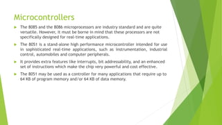
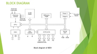
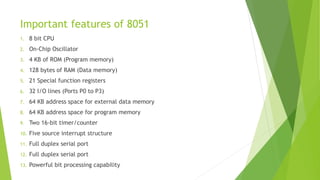
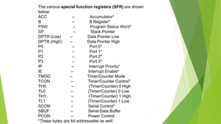
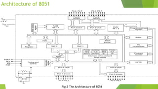
The 8051 microcontroller is designed for real-time applications like industrial control and automobiles. It has features like interrupts, bit addressability, and an enhanced instruction set that make it powerful and cost-effective. The 8051 has 4KB of internal ROM, 128 bytes of internal RAM, 32 I/O lines, and can access up to 64KB each of external program and data memory. It has various special function registers that control timers, serial ports, and interrupts to interface with peripherals. The 8051's architecture includes a CPU, program memory, data memory, ports, and special function registers connected via an internal bus.
2. Microcontrollers
The 8085 and the 8086 microprocessors are industry standard and are quite
versatile. However, it must be borne in mind that these processors are not
specifically designed for real-time applications.
The 8051 is a stand-alone high performance microcontroller intended for use
in sophisticated real-time applications, such as instrumentation, industrial
control, automobiles and computer peripherals.
It provides extra features like interrupts, bit addressability, and an enhanced
set of instructions which make the chip very powerful and cost effective.
The 8051 may be used as a controller for many applications that require up to
64 KB of program memory and/or 64 KB of data memory.
4. Important features of 8051
1. 8 bit CPU
2. On-Chip Oscillator
3. 4 KB of ROM (Program memory)
4. 128 bytes of RAM (Data memory)
5. 21 Special function registers
6. 32 I/O lines (Ports P0 to P3)
7. 64 KB address space for external data memory
8. 64 KB address space for program memory
9. Two 16-bit timer/counter
10. Five source interrupt structure
11. Full duplex serial port
12. Full duplex serial port
13. Powerful bit processing capability
5. Memory Organization
The 8051 can access up to 64 KB of program memory and 64 KB of external
data memory and also the internal data RAM locations.
The separation of code and data memory in the 8051 is different from the
usual von Neumann architecture, which defines that code and data can share
the common memory. The separated memory architecture is referred to as
Harvard architecture.
Memory mapping in 8051
6. Program memory
The processor will come to know whether the user wants to use the internal
ROM or not from the status of the 𝐄𝐀 pin.
If this pin is pulled low, it means that the user does not want to use the
internal ROM available. Hence, the processor will access 0000–FFFFH from the
external program memory.
If this pin is held high, the processor will access addresses 0000–0FFFH from
the internal ROM and as the address goes above 0FFFH, it will access the
external program memory that is interfaced with it.
If 𝐄𝐀= 0 V, External program memory = 0000–FFFFH (64K) If 𝐄𝐀= 5 V Internal
program memory (ROM) = 0000–0FFFH (4K) External program memory = 1000–
FFFFH (60K)
7. Data Memory
The 8051 can access 64 KB of the external data memory and 128 bytes of the
internal data RAM and also 21 special function registers.
For accessing the external data memory, the processor can either issue an 8-bit
address or a 16-bit address. To access the internal data memory, the 8-bit
address is used.
This 8-bit address can provide address spaces for 256 locations. The lower 128
addresses (0 to 127) are used as 128 bytes on-chip RAM and the upper part of the
address space, i.e. (128 to 255) is used to address the various special function
registers.
The lowest 32 bytes (0–31) are reserved for 4 banks of 8 registers, each R0–R7,
out of which one bank may be used at any time. Now the question that arises is,
which bank of registers is being addressed at a particular time?
Answer: Through Program Status Word (PSW).
Memory locations 20H to 2FH are bit addressable too. The address of the bits in
each byte is shown in Figure 5. Memory locations 30H–7FH are general purpose
internal RAM locations. These bytes are not bit addressable.
11. Special Function Registers
All the resources in the 8051 can be accessed through special function registers
maintained in the internal data memory. The resources like timers would require setting
the modes and controlling them. Similarly, serial data input would require a serial data
buffer as well as the control.
The 8051 offers 4 ports which can be used for various purposes like input/output,
memory interface, and so on. The functions of these resources can also be programmed
through special function registers.
There are 21 special function registers in the 8051. Some special function registers are
bit addressable.
12. The various special function registers (SFR) are shown
below:
ACC......................–.............Accumulator*
B...........................–.............B Register*
PSW......................–.............Program Status Word*
SP..........................–.............Stack Pointer
DPTR (Low)........–.............Data Pointer Low
DPTR (High).......–.............Data Pointer High
P0.........................–.............Port 0*
P1.........................–.............Port 1*
P2.........................–.............Port 2*
P3.........................–.............Port 3*
IP..........................–.............Interrupt Priority*
IE.........................–.............Interrupt Enable*
TMOD.................–.............Timer/Counter Mode
TCON..................–.............Timer/Counter Control*
TH0......................–.............(Timer/Counter) 0 High
TL0......................–.............(Timer/Counter) 0 Low
TH1......................–.............(Timer/Counter) 1 High
TL1......................–.............(Timer/Counter) 1 Low
SCON..................–.............Serial Control*
SBUF...................–.............Serial Data Buffer
PCON..................–.............Power Control
*These bytes are bit addressable as well.
13. 1. Accumulator: ACC (also called A register) is the accumulator. There are many
instructions that use the accumulator as the destination. In nearly all arithmetic
operations, ACC is used as one of the operands and after the operation, the result is also
stored in the ACC.
2. B Register: This register is mainly used for multiply and divide operations in which
this register acts as one of the operands and after the operations a part of the result is
stored in this register. This register otherwise is just like a scratch pad, i.e. a temporary
register.
3. Stack Pointer: The stack pointer in the 8051 is an 8-bit wide register. This pointer can
point to any location in the internal data RAM, i.e. locations from 0–127. When the
chip is reset, this register is initialized to 07H. During PUSH and CALL instructions the
stack pointer is first incremented and then the data is stored in the stack. That is, if
initially (SP) = 20H, then the first bytes of the data will be stored at the 21H address.
4. Data Pointer: The data pointer (DPTR) is a 16-bit register, consisting of a high byte
(DPH) and a low byte (DPL). This register normally contains a 16-bit address.
14. 5. Ports 0–3: There are 4 bidirectional input/output ports of 8 bits each. These are directly
represented as pins of the 8051 chips and are bit addressable. These are multifunctional
resources that can be programmed based on the application needs, for example
P0 and P2 can be used as I/O ports or address lines for external memory.
P1 can be used as I/O port. It plays an important role in programming of internal memory of
the 8751 and the 8051.
P3 can be used as I/O port. Its pins have other important alternate functions like Serial Input
Line (P3.0), Serial Output Line (P3.1), External Interrupt Lines (P3.2, P3.3), External Timer
Input Lines (P3.4, P3.5), External Data Memory Write Strobe (P3.6) and External Data
Memory Read Strobe (P3.7).
6. Serial Data Buffer (SBUF): This register holds the data that has to be transmitted
through the serial port and also holds the data that is received. This register is
interconnected to two 8-bit shift registers. When the data is written into the SBUF, it is
loaded in the transmit shift register and hence the process of moving a data byte into the
SBUF starts the transmission process. During reception, the data coming to the 8051 is
clocked into the receive shift register and once all the 8 bits of data or a frame is
received, it is transferred to the SBUF.
15. 7. Control and status registers: All the
special function registers (like IP, IE,
TMOD, TCON, PCON, SCON, etc.) that
are used for controlling the internal
resources or to see the status of these
resources come under this category.
These registers contain the control and
status bits of the interrupt systems,
timers, and serial port operations. The
bit addresses of various special
function registers are shown in the
following figure.
Fig.4 BIT addresses for SFR
17. The instruction decoding and control signal generation are performed using the Timing and Control
circuit block. The bidirectional ports P0 to P3 have the basic structure containing drivers and latches.
The port drivers are connected to I/O ports, whereas the latches are connected to the internal bus of
the microcontroller.
The 8051 contains 128 bytes RAM as data memory and 4 KB ROM as program memory on the chip.
Internal data RAM with address register is connected to the internal bus. The address register will get
the address from the internal bus and the data will be transferred to the specified register through the
bus.
In order to access the internal program memory (ROM) as well as the external program memory, the
program address register is interfaced to program counter which, in turn, is connected to the
incrementer circuit for incrementing the PC. A bidirectional buffer has been provided to temporarily
store the branch address as well as the operand address information. This will also facilitate the
transfer of the program counter contents to other circuits to calculate the PC relative jump address.
Ports P0 and P2 also facilitate the connection to the external memory. The lower-order address bits (A0
to A7) are sent through Port 0 (P0.0 to P0.7) and the higher order address bits (A8 to A15) are sent
through Port 2 (P2.0 to P2.7). P0 also functions as data bus during external read/write in a time
multiplexed manner which is same as in the 8085. Data pointer register (DPTR) is interfaced to the
address register. It plays a major role in external program and data memory addressing using MOVC and
MOVX instructions.
18. Two temporary registers TMP1 and TMP2 are connected to ALU. These
registers hold the operands for calculation. The PSW register is directly
interfaced to ALU for updation on the basis of the last operation.
Port 3 pins are used for input/output for serial I/O (P3.0 and P3.1), external
interrupt inputs (P3.2 and P3.3), timer inputs (P3.4 and P3.5) and external
data memory write and read strobes (P3.6 and P3.7). These are alternate
function pins. Thus, Port 3 can be used purely as I/O port, if these functions
are not required. There is an alternate connection of Port 3 drivers to timer,
interrupt and serial port circuit blocks. The specific special function registers
to program and control these functions are contained in these circuit blocks.
19.
20. References
• Kant, Krishna. Microprocessors and Microcontrollers:
Architecture, Programming and System Design 8085, 8086,
8051, 8096. PHI Learning Pvt. Ltd., 2007.