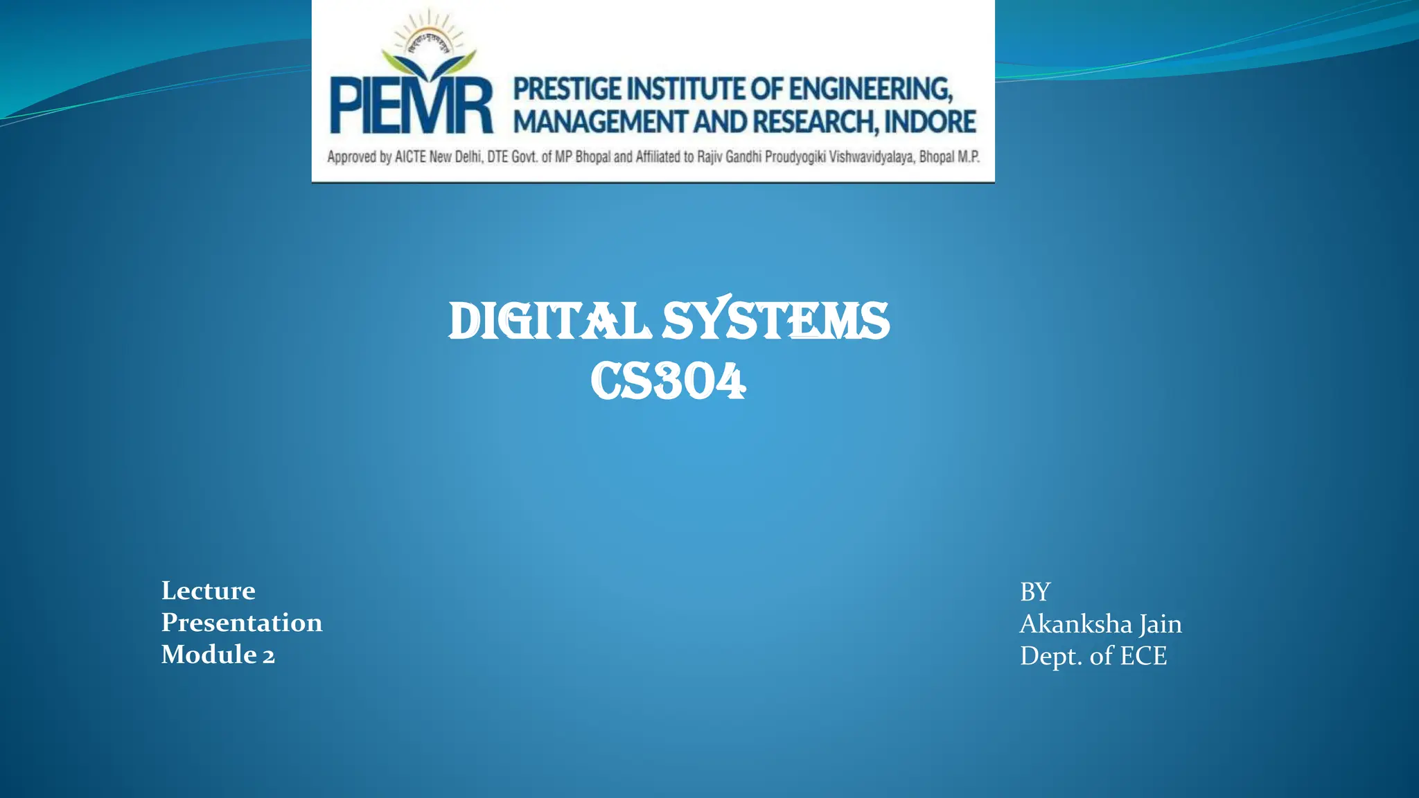
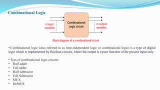
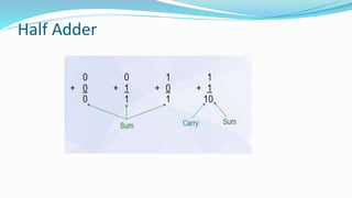
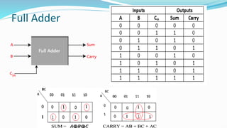
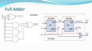
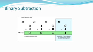
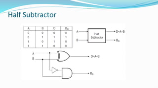
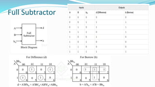
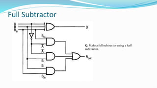
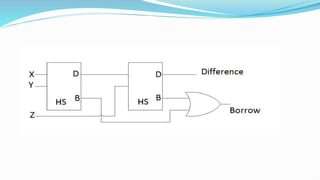
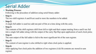
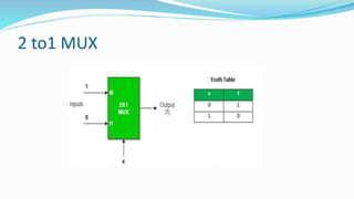
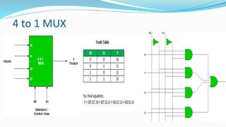
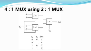
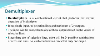
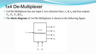
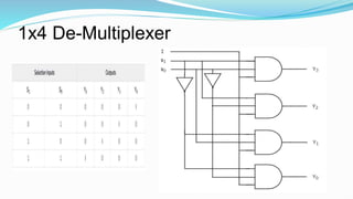
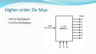
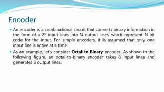
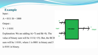
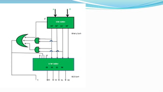
SlideShare a Scribd company logo
Digital Systems
CS304
BY
Akanksha Jain
Dept. of ECE
Lecture
Presentation
Module 2
Combinational Logic
• Combinational logic (also referred to as time-independent logic or combinatorial logic) is a type of digital
logic which is implemented by Boolean circuits, where the output is a pure function of the present input only.
• Tyes of combinational logic circuits:
• Half adder
• Full adder
• Half subtractor
• Full Subtractor
• MUX
• DeMUX
Half Adder
Half Adder
Full Adder
Full Adder
Binary Subtraction
Half Subtractor
Full Subtractor
Full Subtractor
Q. Make a full subtractor using 2 half
subtractor.
Serial Adder
 Working Process:
Following is the procedure of addition using serial binary adder:
• Step-1:
The two shift registers A and B are used to store the numbers to be added.
• Step-2:
A single full adder is used too add one pair of bits at a time along with the carry.
• Step-3:
The contents of the shift registers shift from left to right and their output starting from a and b are fed
into a single full adder along with the output of the carry flip-flop upon application of each clock pulse.
• Step-4:
The sum output of the full adder is fed to the most significant bit of the sum register.
• Step-5:
The content of sum register is also shifted to right when clock pulse is applied.
• Step-6:
After applying four clock pulse the addition of two registers (A & B) contents are stored in sum
register.
Serial Adder
 Serial binary adder is a combinational logic circuit that performs the
addition of two binary numbers in serial form. Serial binary adder performs
bit by bit addition. Two shift registers are used to store the binary numbers
that are to be added.
 A single full adder is used to add one pair of bits at a time along with the
carry. The carry output from the full adder is applied to a D flip-flop
(Memory element). After that output is used as carry for next significant bits.
The sum bit from the output of the full adder can be transferred into a third
shift register.
Serial Adder
 Shift Registers :
Shift Register is a group of flip flops used to store multiple bits of data.
There are two shift registers used in the serial binary adder. In one shift
register augend is stored and in other shift register addend is stored.
 Full Adder :
Full adder is the combinational circuit which takes three inputs and
gives two outputs as sum and carry. The circuit adds one pair at a time
with the help of it.
 D Flip-flop :
the carry output from the full adder is applied on the D flip-flop.
Further, the output of D flip-flop is used as a carry input for the next
pair of significant bits.
Parallel Adder
A single full adder performs the addition of two one bit numbers and an input carry.
But a Parallel Adder is a digital circuit capable of finding the arithmetic sum of
two binary numbers that is greater than one bit in length by operating on
corresponding pairs of bits in parallel.
It consists of full adders connected in a chain where the output carry from each
full adder is connected to the carry input of the next higher order full adder in the
chain.
A n bit parallel adder requires n full adders to perform the operation. So for the
two-bit number, two adders are needed while for four bit number, four adders are
needed and so on. Parallel adders normally incorporate carry lookahead logic to
ensure that carry propagation between subsequent stages of addition does not limit
addition speed. addition speed.
Parallel Adder
 As shown in the figure, firstly the full adder FA1 adds A1 and B1 along with the carry C1 to
generate the sum S1 (the first bit of the output sum) and the carry C2 which is connected to
the next adder in chain.
 As shown in the figure, firstly the full adder FA1 adds A1 and B1 along with the carry C1 to
generate the sum S1 (the first bit of the output sum) and the carry C2 which is connected to
the next adder in chain.
 As shown in the figure, firstly the full adder FA1 adds A1 and B1 along with the carry C1 to
generate the sum S1 (the first bit of the output sum) and the carry C2 which is connected to
the next adder in chain.
Difference between Serial Adder and Parallel Adder:
Multiplexer
 In electronics, a multiplexer (or mux; spelled sometimes as multiplexor),
also known as a data selector, is a device that selects between several
analog or digital input signals and forwards the selected input to a
single output line.
 For N input lines, log n (base2) selection lines, or we can say that for
2n input lines, n selection lines are required.
 Multiplexers are also known as “Data selector, parallel to serial
convertor, many to one circuit, universal logic circuit​”.
 Multiplexers are mainly used to increase amount of the data that can be
sent over the network within certain amount of time and bandwidth.
2 to1 MUX
4 to 1 MUX
4 : 1 MUX using 2 : 1 MUX
Demultiplexer
 De-Multiplexer is a combinational circuit that performs the reverse
operation of Multiplexer.
 It has single input, ‘n’ selection lines and maximum of 2n outputs.
 The input will be connected to one of these outputs based on the values of
selection lines.
 Since there are ‘n’ selection lines, there will be 2n possible combinations
of zeros and ones. So, each combination can select only one output.
1x4 De-Multiplexer
 1x4 De-Multiplexer has one input I, two selection lines, s1 & s0 and four outputs
Y3, Y2, Y1 &Y0.
 The block diagram of 1x4 De-Multiplexer is shown in the following figure.
1x4 De-Multiplexer
Higher order De Mux
• 1x8 De-Multiplexer
• 1x16 De-Multiplexer
Higher order DeMux
Encoder
 An encoder is a combinational circuit that converts binary information in
the form of a 2N input lines into N output lines, which represent N bit
code for the input. For simple encoders, it is assumed that only one
input line is active at a time.
 As an example, let’s consider Octal to Binary encoder. As shown in the
following figure, an octal-to-binary encoder takes 8 input lines and
generates 3 output lines.
Encoder
Encoder
 Implementation –
From the truth table, the output line Z is active when the input octal digit is 1, 3,
5 or 7. Similarly, Y is 1 when input octal digit is 2, 3, 6 or 7 and X is 1 for input
octal.
igits 4, 5, 6 or 7. Hence, the Boolean functions would be:
X = D4 + D5 + D6 + D7
Y = D2 + D3 + D6 + D7
Z = D1 + D3 + D5 + D7
Decoder
 A binary decoder is a digital circuit that converts a binary code into a set
of outputs.
 The binary code represents the position of the desired output and is
used to select the specific output that is active. Binary decoders are the
inverse of encoders and are commonly used in digital systems to
convert a serial code into a parallel set of outputs.
 The basic principle of a binary decoder is to assign a unique output to
each possible binary code.
 For example, a binary decoder with 4 inputs and 2^4 = 16 outputs can
assign a unique output to each of the 16 possible 4-bit binary codes.
Decoder
Decoder
 2-to-4 Binary Decoder –
BCD Adder
• BCD stands for binary coded decimal. It is used to perform the addition of BCD numbers.
• A BCD digit can have any of ten possible four-bit representations. Suppose, we have two 4-
bit numbers A and B. The value of A and B can vary from 0(0000 in binary) to 9(1001 in
binary) because we are considering decimal numbers.
• The output will vary from 0 to 18 if we are not considering the carry from the previous sum.
But if we are considering the carry, then the maximum value of output will be 19 (i.e. 9+9+1
= 19).
• When we are simply adding A and B, then we get the binary sum. Here, to get the output in
BCD form, we will use BCD Adder.
Example
Input :
A = 0111 B = 1000
Output :
Y = 1 0101
Explanation: We are adding A(=7) and B(=8). The
value of binary sum will be 1111(=15). But, the BCD
sum will be 1 0101, where 1 is 0001 in binary and 5
is 0101 in binary.
ALOO
ALU
An arithmetic-logic unit is the part of a central processing unit that carries
out arithmetic and logic operations on the operands in
computer instruction words.
In some processors, the ALU is divided into two units: an arithmetic unit
(AU) and a logic unit (LU). Some processors contain more than one AU --
for example, one for fixed-point operations and another for floating-point
operations.
In computer systems, floating-point computations are sometimes done by
a floating-point unit (FPU) on a separate chip called a numeric coprocessor.

More Related Content

Similar to Lect 1 unit 2.pdf

Combinational and sequential logic
Combinational and sequential logicCombinational and sequential logic
Combinational and sequential logic
Deepak John
 
Combinational circuits
Combinational circuitsCombinational circuits
Combinational circuits
Nabarun Chakraborty
 
combinational_circuits
combinational_circuitscombinational_circuits
combinational_circuitsBindu Madhavi
 
combinational_circuits
combinational_circuitscombinational_circuits
combinational_circuitsBindu Madhavi
 
Chapter-04.pdf
Chapter-04.pdfChapter-04.pdf
Chapter-04.pdf
ssuserf7cd2b
 
CHAPTER 6: Function of Combination Logic From Flyod ( Digital Logic Design )
CHAPTER 6: Function of Combination Logic From Flyod ( Digital Logic Design ) CHAPTER 6: Function of Combination Logic From Flyod ( Digital Logic Design )
CHAPTER 6: Function of Combination Logic From Flyod ( Digital Logic Design )
Sefat Ahammed Shovo
 
B sc3 unit 4 combi..lckt
B sc3 unit 4 combi..lcktB sc3 unit 4 combi..lckt
B sc3 unit 4 combi..lckt
MahiboobAliMulla
 
DCF-Combinational circuit
DCF-Combinational circuitDCF-Combinational circuit
DCF-Combinational circuit
vinothinisureshbabu
 
Combinational Circuits.pptx
Combinational Circuits.pptxCombinational Circuits.pptx
Combinational Circuits.pptx
AshokRachapalli1
 
Four bit Signed Calculator.pptx
Four bit Signed Calculator.pptxFour bit Signed Calculator.pptx
Four bit Signed Calculator.pptx
SUGAMRAJPUT2
 
Chapter 4: Combinational Logic
Chapter 4: Combinational LogicChapter 4: Combinational Logic
Chapter 4: Combinational Logic
Er. Nawaraj Bhandari
 
Parallel Adder_Mul_Mag.pptx
Parallel Adder_Mul_Mag.pptxParallel Adder_Mul_Mag.pptx
Parallel Adder_Mul_Mag.pptx
PreetamKalyaan
 
CSO PPT.pptx
CSO PPT.pptxCSO PPT.pptx
CSO PPT.pptx
PranjalTripathi19
 
Combinational circuit
Combinational circuitCombinational circuit
Combinational circuit
SIVALAKSHMIPANNEERSE
 
Computer Organization and Architecture Presentation
Computer Organization and Architecture PresentationComputer Organization and Architecture Presentation
Computer Organization and Architecture Presentation
ChiragBhardwaj52
 
COMPUTER ORGANIZATION NOTES Unit 6
COMPUTER ORGANIZATION NOTES Unit 6COMPUTER ORGANIZATION NOTES Unit 6
COMPUTER ORGANIZATION NOTES Unit 6
Dr.MAYA NAYAK
 
Arithmetic Microoperation.pdf
Arithmetic Microoperation.pdfArithmetic Microoperation.pdf
Arithmetic Microoperation.pdf
HarshitJ4
 
DLD Lecture No 20 Look Ahead Carry Generator, Binary Subtractors and BCD Add...
DLD Lecture No 20 Look Ahead Carry Generator, Binary Subtractors and  BCD Add...DLD Lecture No 20 Look Ahead Carry Generator, Binary Subtractors and  BCD Add...
DLD Lecture No 20 Look Ahead Carry Generator, Binary Subtractors and BCD Add...
SaveraAyub2
 
Adder and subtrctor DLD
Adder and subtrctor  DLDAdder and subtrctor  DLD
Adder and subtrctor DLD
Rokonuzzaman Rony
 
Combinational circuits r011
Combinational circuits   r011Combinational circuits   r011
Combinational circuits r011
arunachalamr16
 

Similar to Lect 1 unit 2.pdf (20)

Combinational and sequential logic
Combinational and sequential logicCombinational and sequential logic
Combinational and sequential logic
 
Combinational circuits
Combinational circuitsCombinational circuits
Combinational circuits
 
combinational_circuits
combinational_circuitscombinational_circuits
combinational_circuits
 
combinational_circuits
combinational_circuitscombinational_circuits
combinational_circuits
 
Chapter-04.pdf
Chapter-04.pdfChapter-04.pdf
Chapter-04.pdf
 
CHAPTER 6: Function of Combination Logic From Flyod ( Digital Logic Design )
CHAPTER 6: Function of Combination Logic From Flyod ( Digital Logic Design ) CHAPTER 6: Function of Combination Logic From Flyod ( Digital Logic Design )
CHAPTER 6: Function of Combination Logic From Flyod ( Digital Logic Design )
 
B sc3 unit 4 combi..lckt
B sc3 unit 4 combi..lcktB sc3 unit 4 combi..lckt
B sc3 unit 4 combi..lckt
 
DCF-Combinational circuit
DCF-Combinational circuitDCF-Combinational circuit
DCF-Combinational circuit
 
Combinational Circuits.pptx
Combinational Circuits.pptxCombinational Circuits.pptx
Combinational Circuits.pptx
 
Four bit Signed Calculator.pptx
Four bit Signed Calculator.pptxFour bit Signed Calculator.pptx
Four bit Signed Calculator.pptx
 
Chapter 4: Combinational Logic
Chapter 4: Combinational LogicChapter 4: Combinational Logic
Chapter 4: Combinational Logic
 
Parallel Adder_Mul_Mag.pptx
Parallel Adder_Mul_Mag.pptxParallel Adder_Mul_Mag.pptx
Parallel Adder_Mul_Mag.pptx
 
CSO PPT.pptx
CSO PPT.pptxCSO PPT.pptx
CSO PPT.pptx
 
Combinational circuit
Combinational circuitCombinational circuit
Combinational circuit
 
Computer Organization and Architecture Presentation
Computer Organization and Architecture PresentationComputer Organization and Architecture Presentation
Computer Organization and Architecture Presentation
 
COMPUTER ORGANIZATION NOTES Unit 6
COMPUTER ORGANIZATION NOTES Unit 6COMPUTER ORGANIZATION NOTES Unit 6
COMPUTER ORGANIZATION NOTES Unit 6
 
Arithmetic Microoperation.pdf
Arithmetic Microoperation.pdfArithmetic Microoperation.pdf
Arithmetic Microoperation.pdf
 
DLD Lecture No 20 Look Ahead Carry Generator, Binary Subtractors and BCD Add...
DLD Lecture No 20 Look Ahead Carry Generator, Binary Subtractors and  BCD Add...DLD Lecture No 20 Look Ahead Carry Generator, Binary Subtractors and  BCD Add...
DLD Lecture No 20 Look Ahead Carry Generator, Binary Subtractors and BCD Add...
 
Adder and subtrctor DLD
Adder and subtrctor  DLDAdder and subtrctor  DLD
Adder and subtrctor DLD
 
Combinational circuits r011
Combinational circuits   r011Combinational circuits   r011
Combinational circuits r011
 

Recently uploaded

block diagram and signal flow graph representation
block diagram and signal flow graph representationblock diagram and signal flow graph representation
block diagram and signal flow graph representation
Divya Somashekar
 
Cosmetic shop management system project report.pdf
Cosmetic shop management system project report.pdfCosmetic shop management system project report.pdf
Cosmetic shop management system project report.pdf
Kamal Acharya
 
Industrial Training at Shahjalal Fertilizer Company Limited (SFCL)
Industrial Training at Shahjalal Fertilizer Company Limited (SFCL)Industrial Training at Shahjalal Fertilizer Company Limited (SFCL)
Industrial Training at Shahjalal Fertilizer Company Limited (SFCL)
MdTanvirMahtab2
 
Halogenation process of chemical process industries
Halogenation process of chemical process industriesHalogenation process of chemical process industries
Halogenation process of chemical process industries
MuhammadTufail242431
 
weather web application report.pdf
weather web application report.pdfweather web application report.pdf
weather web application report.pdf
Pratik Pawar
 
road safety engineering r s e unit 3.pdf
road safety engineering  r s e unit 3.pdfroad safety engineering  r s e unit 3.pdf
road safety engineering r s e unit 3.pdf
VENKATESHvenky89705
 
CME397 Surface Engineering- Professional Elective
CME397 Surface Engineering- Professional ElectiveCME397 Surface Engineering- Professional Elective
CME397 Surface Engineering- Professional Elective
karthi keyan
 
Event Management System Vb Net Project Report.pdf
Event Management System Vb Net  Project Report.pdfEvent Management System Vb Net  Project Report.pdf
Event Management System Vb Net Project Report.pdf
Kamal Acharya
 
J.Yang, ICLR 2024, MLILAB, KAIST AI.pdf
J.Yang,  ICLR 2024, MLILAB, KAIST AI.pdfJ.Yang,  ICLR 2024, MLILAB, KAIST AI.pdf
J.Yang, ICLR 2024, MLILAB, KAIST AI.pdf
MLILAB
 
一比一原版(SFU毕业证)西蒙菲莎大学毕业证成绩单如何办理
一比一原版(SFU毕业证)西蒙菲莎大学毕业证成绩单如何办理一比一原版(SFU毕业证)西蒙菲莎大学毕业证成绩单如何办理
一比一原版(SFU毕业证)西蒙菲莎大学毕业证成绩单如何办理
bakpo1
 
Vaccine management system project report documentation..pdf
Vaccine management system project report documentation..pdfVaccine management system project report documentation..pdf
Vaccine management system project report documentation..pdf
Kamal Acharya
 
Railway Signalling Principles Edition 3.pdf
Railway Signalling Principles Edition 3.pdfRailway Signalling Principles Edition 3.pdf
Railway Signalling Principles Edition 3.pdf
TeeVichai
 
Nuclear Power Economics and Structuring 2024
Nuclear Power Economics and Structuring 2024Nuclear Power Economics and Structuring 2024
Nuclear Power Economics and Structuring 2024
Massimo Talia
 
addressing modes in computer architecture
addressing modes  in computer architectureaddressing modes  in computer architecture
addressing modes in computer architecture
ShahidSultan24
 
Top 10 Oil and Gas Projects in Saudi Arabia 2024.pdf
Top 10 Oil and Gas Projects in Saudi Arabia 2024.pdfTop 10 Oil and Gas Projects in Saudi Arabia 2024.pdf
Top 10 Oil and Gas Projects in Saudi Arabia 2024.pdf
Teleport Manpower Consultant
 
Quality defects in TMT Bars, Possible causes and Potential Solutions.
Quality defects in TMT Bars, Possible causes and Potential Solutions.Quality defects in TMT Bars, Possible causes and Potential Solutions.
Quality defects in TMT Bars, Possible causes and Potential Solutions.
PrashantGoswami42
 
HYDROPOWER - Hydroelectric power generation
HYDROPOWER - Hydroelectric power generationHYDROPOWER - Hydroelectric power generation
HYDROPOWER - Hydroelectric power generation
Robbie Edward Sayers
 
Pile Foundation by Venkatesh Taduvai (Sub Geotechnical Engineering II)-conver...
Pile Foundation by Venkatesh Taduvai (Sub Geotechnical Engineering II)-conver...Pile Foundation by Venkatesh Taduvai (Sub Geotechnical Engineering II)-conver...
Pile Foundation by Venkatesh Taduvai (Sub Geotechnical Engineering II)-conver...
AJAYKUMARPUND1
 
Architectural Portfolio Sean Lockwood
Architectural Portfolio Sean LockwoodArchitectural Portfolio Sean Lockwood
Architectural Portfolio Sean Lockwood
seandesed
 
AKS UNIVERSITY Satna Final Year Project By OM Hardaha.pdf
AKS UNIVERSITY Satna Final Year Project By OM Hardaha.pdfAKS UNIVERSITY Satna Final Year Project By OM Hardaha.pdf
AKS UNIVERSITY Satna Final Year Project By OM Hardaha.pdf
SamSarthak3
 

Recently uploaded (20)

block diagram and signal flow graph representation
block diagram and signal flow graph representationblock diagram and signal flow graph representation
block diagram and signal flow graph representation
 
Cosmetic shop management system project report.pdf
Cosmetic shop management system project report.pdfCosmetic shop management system project report.pdf
Cosmetic shop management system project report.pdf
 
Industrial Training at Shahjalal Fertilizer Company Limited (SFCL)
Industrial Training at Shahjalal Fertilizer Company Limited (SFCL)Industrial Training at Shahjalal Fertilizer Company Limited (SFCL)
Industrial Training at Shahjalal Fertilizer Company Limited (SFCL)
 
Halogenation process of chemical process industries
Halogenation process of chemical process industriesHalogenation process of chemical process industries
Halogenation process of chemical process industries
 
weather web application report.pdf
weather web application report.pdfweather web application report.pdf
weather web application report.pdf
 
road safety engineering r s e unit 3.pdf
road safety engineering  r s e unit 3.pdfroad safety engineering  r s e unit 3.pdf
road safety engineering r s e unit 3.pdf
 
CME397 Surface Engineering- Professional Elective
CME397 Surface Engineering- Professional ElectiveCME397 Surface Engineering- Professional Elective
CME397 Surface Engineering- Professional Elective
 
Event Management System Vb Net Project Report.pdf
Event Management System Vb Net  Project Report.pdfEvent Management System Vb Net  Project Report.pdf
Event Management System Vb Net Project Report.pdf
 
J.Yang, ICLR 2024, MLILAB, KAIST AI.pdf
J.Yang,  ICLR 2024, MLILAB, KAIST AI.pdfJ.Yang,  ICLR 2024, MLILAB, KAIST AI.pdf
J.Yang, ICLR 2024, MLILAB, KAIST AI.pdf
 
一比一原版(SFU毕业证)西蒙菲莎大学毕业证成绩单如何办理
一比一原版(SFU毕业证)西蒙菲莎大学毕业证成绩单如何办理一比一原版(SFU毕业证)西蒙菲莎大学毕业证成绩单如何办理
一比一原版(SFU毕业证)西蒙菲莎大学毕业证成绩单如何办理
 
Vaccine management system project report documentation..pdf
Vaccine management system project report documentation..pdfVaccine management system project report documentation..pdf
Vaccine management system project report documentation..pdf
 
Railway Signalling Principles Edition 3.pdf
Railway Signalling Principles Edition 3.pdfRailway Signalling Principles Edition 3.pdf
Railway Signalling Principles Edition 3.pdf
 
Nuclear Power Economics and Structuring 2024
Nuclear Power Economics and Structuring 2024Nuclear Power Economics and Structuring 2024
Nuclear Power Economics and Structuring 2024
 
addressing modes in computer architecture
addressing modes  in computer architectureaddressing modes  in computer architecture
addressing modes in computer architecture
 
Top 10 Oil and Gas Projects in Saudi Arabia 2024.pdf
Top 10 Oil and Gas Projects in Saudi Arabia 2024.pdfTop 10 Oil and Gas Projects in Saudi Arabia 2024.pdf
Top 10 Oil and Gas Projects in Saudi Arabia 2024.pdf
 
Quality defects in TMT Bars, Possible causes and Potential Solutions.
Quality defects in TMT Bars, Possible causes and Potential Solutions.Quality defects in TMT Bars, Possible causes and Potential Solutions.
Quality defects in TMT Bars, Possible causes and Potential Solutions.
 
HYDROPOWER - Hydroelectric power generation
HYDROPOWER - Hydroelectric power generationHYDROPOWER - Hydroelectric power generation
HYDROPOWER - Hydroelectric power generation
 
Pile Foundation by Venkatesh Taduvai (Sub Geotechnical Engineering II)-conver...
Pile Foundation by Venkatesh Taduvai (Sub Geotechnical Engineering II)-conver...Pile Foundation by Venkatesh Taduvai (Sub Geotechnical Engineering II)-conver...
Pile Foundation by Venkatesh Taduvai (Sub Geotechnical Engineering II)-conver...
 
Architectural Portfolio Sean Lockwood
Architectural Portfolio Sean LockwoodArchitectural Portfolio Sean Lockwood
Architectural Portfolio Sean Lockwood
 
AKS UNIVERSITY Satna Final Year Project By OM Hardaha.pdf
AKS UNIVERSITY Satna Final Year Project By OM Hardaha.pdfAKS UNIVERSITY Satna Final Year Project By OM Hardaha.pdf
AKS UNIVERSITY Satna Final Year Project By OM Hardaha.pdf
 

Lect 1 unit 2.pdf

  • 1. Digital Systems CS304 BY Akanksha Jain Dept. of ECE Lecture Presentation Module 2
  • 2. Combinational Logic • Combinational logic (also referred to as time-independent logic or combinatorial logic) is a type of digital logic which is implemented by Boolean circuits, where the output is a pure function of the present input only. • Tyes of combinational logic circuits: • Half adder • Full adder • Half subtractor • Full Subtractor • MUX • DeMUX
  • 10. Full Subtractor Q. Make a full subtractor using 2 half subtractor.
  • 11.
  • 12. Serial Adder  Working Process: Following is the procedure of addition using serial binary adder: • Step-1: The two shift registers A and B are used to store the numbers to be added. • Step-2: A single full adder is used too add one pair of bits at a time along with the carry. • Step-3: The contents of the shift registers shift from left to right and their output starting from a and b are fed into a single full adder along with the output of the carry flip-flop upon application of each clock pulse. • Step-4: The sum output of the full adder is fed to the most significant bit of the sum register. • Step-5: The content of sum register is also shifted to right when clock pulse is applied. • Step-6: After applying four clock pulse the addition of two registers (A & B) contents are stored in sum register.
  • 13. Serial Adder  Serial binary adder is a combinational logic circuit that performs the addition of two binary numbers in serial form. Serial binary adder performs bit by bit addition. Two shift registers are used to store the binary numbers that are to be added.  A single full adder is used to add one pair of bits at a time along with the carry. The carry output from the full adder is applied to a D flip-flop (Memory element). After that output is used as carry for next significant bits. The sum bit from the output of the full adder can be transferred into a third shift register.
  • 14. Serial Adder  Shift Registers : Shift Register is a group of flip flops used to store multiple bits of data. There are two shift registers used in the serial binary adder. In one shift register augend is stored and in other shift register addend is stored.  Full Adder : Full adder is the combinational circuit which takes three inputs and gives two outputs as sum and carry. The circuit adds one pair at a time with the help of it.  D Flip-flop : the carry output from the full adder is applied on the D flip-flop. Further, the output of D flip-flop is used as a carry input for the next pair of significant bits.
  • 15. Parallel Adder A single full adder performs the addition of two one bit numbers and an input carry. But a Parallel Adder is a digital circuit capable of finding the arithmetic sum of two binary numbers that is greater than one bit in length by operating on corresponding pairs of bits in parallel. It consists of full adders connected in a chain where the output carry from each full adder is connected to the carry input of the next higher order full adder in the chain. A n bit parallel adder requires n full adders to perform the operation. So for the two-bit number, two adders are needed while for four bit number, four adders are needed and so on. Parallel adders normally incorporate carry lookahead logic to ensure that carry propagation between subsequent stages of addition does not limit addition speed. addition speed.
  • 16.
  • 17. Parallel Adder  As shown in the figure, firstly the full adder FA1 adds A1 and B1 along with the carry C1 to generate the sum S1 (the first bit of the output sum) and the carry C2 which is connected to the next adder in chain.  As shown in the figure, firstly the full adder FA1 adds A1 and B1 along with the carry C1 to generate the sum S1 (the first bit of the output sum) and the carry C2 which is connected to the next adder in chain.  As shown in the figure, firstly the full adder FA1 adds A1 and B1 along with the carry C1 to generate the sum S1 (the first bit of the output sum) and the carry C2 which is connected to the next adder in chain.
  • 18. Difference between Serial Adder and Parallel Adder:
  • 19.
  • 20.
  • 21. Multiplexer  In electronics, a multiplexer (or mux; spelled sometimes as multiplexor), also known as a data selector, is a device that selects between several analog or digital input signals and forwards the selected input to a single output line.  For N input lines, log n (base2) selection lines, or we can say that for 2n input lines, n selection lines are required.  Multiplexers are also known as “Data selector, parallel to serial convertor, many to one circuit, universal logic circuit​”.  Multiplexers are mainly used to increase amount of the data that can be sent over the network within certain amount of time and bandwidth.
  • 23. 4 to 1 MUX
  • 24. 4 : 1 MUX using 2 : 1 MUX
  • 25. Demultiplexer  De-Multiplexer is a combinational circuit that performs the reverse operation of Multiplexer.  It has single input, ‘n’ selection lines and maximum of 2n outputs.  The input will be connected to one of these outputs based on the values of selection lines.  Since there are ‘n’ selection lines, there will be 2n possible combinations of zeros and ones. So, each combination can select only one output.
  • 26. 1x4 De-Multiplexer  1x4 De-Multiplexer has one input I, two selection lines, s1 & s0 and four outputs Y3, Y2, Y1 &Y0.  The block diagram of 1x4 De-Multiplexer is shown in the following figure.
  • 28. Higher order De Mux • 1x8 De-Multiplexer • 1x16 De-Multiplexer
  • 30. Encoder  An encoder is a combinational circuit that converts binary information in the form of a 2N input lines into N output lines, which represent N bit code for the input. For simple encoders, it is assumed that only one input line is active at a time.  As an example, let’s consider Octal to Binary encoder. As shown in the following figure, an octal-to-binary encoder takes 8 input lines and generates 3 output lines.
  • 32. Encoder  Implementation – From the truth table, the output line Z is active when the input octal digit is 1, 3, 5 or 7. Similarly, Y is 1 when input octal digit is 2, 3, 6 or 7 and X is 1 for input octal. igits 4, 5, 6 or 7. Hence, the Boolean functions would be: X = D4 + D5 + D6 + D7 Y = D2 + D3 + D6 + D7 Z = D1 + D3 + D5 + D7
  • 33. Decoder  A binary decoder is a digital circuit that converts a binary code into a set of outputs.  The binary code represents the position of the desired output and is used to select the specific output that is active. Binary decoders are the inverse of encoders and are commonly used in digital systems to convert a serial code into a parallel set of outputs.  The basic principle of a binary decoder is to assign a unique output to each possible binary code.  For example, a binary decoder with 4 inputs and 2^4 = 16 outputs can assign a unique output to each of the 16 possible 4-bit binary codes.
  • 36. BCD Adder • BCD stands for binary coded decimal. It is used to perform the addition of BCD numbers. • A BCD digit can have any of ten possible four-bit representations. Suppose, we have two 4- bit numbers A and B. The value of A and B can vary from 0(0000 in binary) to 9(1001 in binary) because we are considering decimal numbers. • The output will vary from 0 to 18 if we are not considering the carry from the previous sum. But if we are considering the carry, then the maximum value of output will be 19 (i.e. 9+9+1 = 19). • When we are simply adding A and B, then we get the binary sum. Here, to get the output in BCD form, we will use BCD Adder.
  • 37. Example Input : A = 0111 B = 1000 Output : Y = 1 0101 Explanation: We are adding A(=7) and B(=8). The value of binary sum will be 1111(=15). But, the BCD sum will be 1 0101, where 1 is 0001 in binary and 5 is 0101 in binary.
  • 38.
  • 39. ALOO
  • 40. ALU
  • 41. An arithmetic-logic unit is the part of a central processing unit that carries out arithmetic and logic operations on the operands in computer instruction words. In some processors, the ALU is divided into two units: an arithmetic unit (AU) and a logic unit (LU). Some processors contain more than one AU -- for example, one for fixed-point operations and another for floating-point operations. In computer systems, floating-point computations are sometimes done by a floating-point unit (FPU) on a separate chip called a numeric coprocessor.