SlideShare a Scribd company logo
UNIT II
COMBINATIONAL LOGIC
• Combinational Circuits –Analysis and Design Procedures
• Binary Adder-Subtractor
• Decimal Adder
• Binary Multiplier
• Magnitude Comparator
• Decoders–Encoders
• Multiplexers
• Introduction to HDL –HDL Models of Combinational circuits.
Introduction:
• When logic gates are connected together to produce a specified output for
certain specified combinations of input variables, with no storage involved, the
resulting circuit is called combinational logic circuit.
• In combinational logic circuit, the output variables are at all times dependent
on the combination of input variables.
• The combinational circuit do not use any memory. The previous state of input
does not have any effect on the present state of the circuit.
• A combinational circuit can have an n number of inputs and m number of
outputs.
Analysis Procedure
Steps to analyse combinational circuit:
1. First make sure that the given circuit is combinational circuit and not the
sequential circuit. The combinational circuit has logic gates with no feedback
path or memory elements.
2. Label all gate outputs that are a function of input variables with arbitrary
symbols and determine the Boolean functions for each gate output.
3. Label the gates that are a function of input variables and previously labelled
gates and determine the Boolean functions for them.
4. Repeat the step 3 until the Boolean function for outputs of the circuit are
obtained.
5. Finally, substituting previously defined Boolean functions, obtain the output
Boolean functions in terms of input variables.
1. Analyze the following logic diagram.
Solution:
𝑇1 = 𝐴
𝑇2 = BC
𝑇3 = 𝑇1. 𝑇5 = 𝐴. 𝐴. 𝐷 = 𝐴. 𝐴 + 𝐷 = 𝐴𝐷
𝑇4 = 𝑇1 + 𝐵𝐶 = 𝐴 + 𝐵𝐶
𝑇5 = 𝐴. 𝐷 = 𝐴 + 𝐷
𝐹 = 𝑇3. 𝑇4 = 𝐴𝐷 . 𝐴 + 𝐵𝐶 = 𝐴𝐷 + 𝐴𝐵𝐶𝐷
= 𝐴𝐷 1 + 𝐵𝐶 = 𝐴𝐷
𝐺 = 𝑇4. 𝑇5 = 𝐴 + 𝐵𝐶 . 𝐴 + 𝐷
= 𝐴A + 𝐴𝐷 + 𝐴𝐵𝐶 + 𝐵𝐶𝐷
A B C D 𝑻𝟏 𝑻𝟐 𝑻𝟑 𝑻𝟒 𝑻𝟓 F G
0 0 0 0 1 0 1 1 1 1 1
0 0 0 1 1 0 0 1 0 0 0
0 0 1 0 1 0 1 1 1 1 1
0 0 1 1 1 0 0 1 0 0 0
0 1 0 0 1 0 1 1 1 1 1
0 1 0 1 1 0 0 1 0 0 0
0 1 1 0 1 1 1 1 1 1 1
0 1 1 1 1 1 0 1 0 0 0
1 0 0 0 0 0 0 0 1 0 0
1 0 0 1 0 0 0 0 1 0 0
1 0 1 0 0 0 0 0 1 0 0
1 0 1 1 0 0 0 0 1 0 0
1 1 0 0 0 0 0 0 1 0 0
1 1 0 1 0 0 0 0 1 0 0
1 1 1 0 0 1 0 0 1 0 1
1 1 1 1 0 1 0 0 1 0 1
Truth Table
𝐴𝐷
K-Map for output F:
𝐴𝐷
𝐴𝐵𝐶
K-Map for output G:
2. Consider the combinational circuit shown.
i)Derive the Boolean expressions for 𝑇1 through 𝑇4.Evaluate the outputs 𝐹1and 𝐹2as
a function of the four inputs.
ii)List the truth table with 16 binary combinations of the four input variables. Then
list the binary values for 𝑇1 through 𝑇4and the outputs 𝐹1and 𝐹2 in the table.
iii)Plot the output Boolean function obtained in part (ii) on maps and show the
simplified Boolean expressions are equivalent to the ones obtained in part (i).
Solution:
• 𝑇1 = 𝐵𝐶
• 𝑇2 = 𝐴𝐵
• 𝑇3 = A + 𝐵C
• 𝑇4 = AD + 𝐵D + 𝐴B𝐷
• 𝐹1 = A + B𝐷 + 𝐵C + 𝐵D
• 𝐹2 = 𝐴B + D
A B C D 𝑻𝟏 𝑻𝟐 𝑻𝟑 𝑻𝟒 𝑭𝟏 𝑭𝟐
0 0 0 0 0 0 0 0 0 0
0 0 0 1 0 0 0 1 1 1
0 0 1 0 1 0 1 0 1 0
0 0 1 1 1 0 1 1 1 1
0 1 0 0 0 1 0 1 1 1
0 1 0 1 0 1 0 0 0 1
0 1 1 0 0 1 0 1 1 1
0 1 1 1 0 1 0 0 0 1
1 0 0 0 0 0 1 0 1 0
1 0 0 1 0 0 1 1 1 1
1 0 1 0 1 0 1 0 1 0
1 0 1 1 1 0 1 1 1 1
1 1 0 0 0 0 1 0 1 0
1 1 0 1 0 0 1 1 1 1
1 1 1 0 0 0 1 0 1 0
1 1 1 1 0 0 1 1 1 1
Truth Table
K-Map for output 𝑭𝟏: K-Map for output 𝑭𝟐:
Design Procedure
Steps to design the combinational circuit
1. The problem definition
2. The determination of number of available input variables and
required output variables.
3. Assigning letter symbols to input and output variables
4. The derivation of truth table indicating the relationships between
input and output variables
5. Obtain simplified Boolean expression for each output
6. Obtain the logic diagram
(i) Explain the design procedure of a combinational circuit.
(ii)The inputs to a circuit are the 4 bits of the binary number D3D2D1D0.The circuit produces a 1 if and only if
all of the following conditions hold
1)MSB is ‘1’or any of the other bits are a ‘0’
2) D2 is a 1 or any of the other bits are a ‘0’.
3)Any of the 4 bits are 0
Obtain a minimal expression for the output
Inputs Output
D3 D2 D1 D0 Y
0 0 0 0 1
0 0 0 1 1
0 0 1 0 1
0 0 1 1 1
0 1 0 0 1
0 1 0 1 1
0 1 1 0 1
0 1 1 1 0
1 0 0 0 1
1 0 0 1 1
1 0 1 0 1
1 0 1 1 0
1 1 0 0 1
1 1 0 1 1
1 1 1 0 1
1 1 1 1 0
Truth Table
D1D0
D3 D2
D1 D0
00
D1D0
01
D1D0
11
D1D0
10
00
D3 D2 0 1 3 2
01
D3D2 4 5 7 6
11
D3D2
12 13 15 14
10
D3D2 8 9 11 10
A majority gate is a digital circuit whose output is equal to 1 if the majority of inputs
are 1’s. The output is 0 otherwise. Using a truth table, find the Boolean function
implemented by a 3-input majority gate. Simplify the function and implement with
gates.
Solution:
Step 1:Derive the truth table Step 2: Obtain the simplified Boolean expression
Step 3: Draw the logic diagram
A B C Y
0 0 0 0
0 0 1 0
0 1 0 0
0 1 1 1
1 0 0 0
1 0 1 1
1 1 0 1
1 1 1 1
BC
A
00
𝐵 𝐶
01
𝐵 C
11
BC
10
B𝐶
0 𝐴 0 1 3 2
1 A 4 5 7 6
Binary Adder Subtractor
Adders:
• The most basic operation, is the addition of two binary digits.
• The simple addition consists of four possible elementary operations, namely,
0+0=0
0+1=1
1+0=1
1+1= 102
• The first three operations produce a sum whose length is one digit, but when the
last operation is performed sum is two digits. The higher significant bit of this
result is called a carry, and lower significant bit is called sum.
• The logic circuit which performs this operation is called a half-adder.
• The circuit which performs addition of three bits is called a full-adder.
11. Design a half adder and full adder.
Two binary inputs: augend and addend bits
Two binary outputs: sum and carry
K-map simplification: Logic diagram:
Inputs Outputs
A B Carry Sum
0 0 0 0
0 1 0 1
1 0 0 1
1 1 1 0
Truth Table for half adder
Block schematic of half adder
B
A 0 𝐵 1 B
0 𝐴 0 0
1 A 0 1
B
A 0 𝐵 1 B
0 𝐴 0 1
1 A 1 0
Carry Sum
Carry=AB Sum=A𝐵 +𝐴𝐵
=A + B
Full Adder
• A full adder is a combinational circuit that forms the arithmetic sum of three input
bits.
• It consist of three inputs and two outputs.
• Two of the input variables, denoted by A and B, represent the two significant bits
to be added. The third input Cin, represents the carry from the previous lower
significant position.
Full adder
A
B
Cin
Cout
Sum
Block Schematic of
full adder
Inputs Outputs
A B Cin
Carry
(Cout)
Sum
0 0 0 0 0
0 0 1 0 1
0 1 0 0 1
0 1 1 1 0
1 0 0 0 1
1 0 1 1 0
1 1 0 1 0
1 1 1 1 1
Truth table of full adder
K-map simplification for carry and sum
BCin
A
00
𝐵 Cin
01
𝐵Cin
11
BCin
10
BCin
0 𝐴 0 0 0 1 1 3 0 2
1 A 0 4 1 5 1 7 1 6
BCin
A
00
𝐵 Cin
01
𝐵Cin
11
BCin
10
BCin
0 𝐴 0 0 1 1 0 3 1 2
1 A 1 4 0 5 1 7 0 6
K-map for Carry (Cout )
K-map for Sum
𝑪𝒐𝒖𝒕 = 𝑨𝑩 + 𝑨𝑪𝒊𝒏 + 𝑩𝑪𝒊𝒏
𝑺𝒖𝒎 = 𝑨𝑩𝑪𝒊𝒏 + 𝑨𝑩𝑪𝒊𝒏+ 𝐀𝑩𝑪𝒊𝒏 + 𝐀𝐁𝑪𝒊𝒏
Implementation using logic gates:
𝑺𝒖𝒎 = 𝑨𝑩𝑪𝒊𝒏 + 𝑨𝑩𝑪𝒊𝒏+ 𝐀𝑩𝑪𝒊𝒏 + 𝐀𝐁𝑪𝒊𝒏
= 𝑪𝒊𝒏(𝑨𝑩 + 𝐀𝐁) + 𝑪𝒊𝒏(𝑨𝑩+ 𝐀𝑩)
= 𝑪𝒊𝒏(𝑨ʘ𝑩) + 𝑪𝒊𝒏(𝑨⨁𝑩)
= 𝑪𝒊𝒏(𝑨⨁𝑩) + 𝑪𝒊𝒏(𝑨⨁𝑩)
𝑺𝒖𝒎 = 𝑪𝒊𝒏⨁(𝑨⨁𝑩)
Full adder using two half adders:
𝑪𝒐𝒖𝒕 = 𝑨𝑩 + 𝑨𝑪𝒊𝒏 + 𝑩𝑪𝒊𝒏
= 𝑨𝑩 + 𝑨𝑪𝒊𝒏 𝑩 + 𝑩 + 𝑩𝑪𝒊𝒏 𝑨 + 𝑨
= 𝑨𝑩 + (𝑨𝑩𝑪𝒊𝒏 + 𝑨𝑩𝑪𝒊𝒏) + 𝑨𝑩𝑪𝒊𝒏 + 𝑨𝑩𝑪𝒊𝒏
= 𝑨𝑩 𝟏 + 𝑪𝒊𝒏 + 𝑪𝒊𝒏 + 𝑨𝑩𝑪𝒊𝒏 + 𝑨𝑩𝑪𝒊𝒏
= 𝑨𝑩 + 𝑨𝑩𝑪𝒊𝒏 + 𝑨𝑩𝑪𝒊𝒏
= 𝑨𝑩 + 𝑪𝒊𝒏 𝑨𝑩 + 𝑨𝑩
𝑪𝒐𝒖𝒕 = 𝑨𝑩 + 𝑪𝒊𝒏 𝑨⨁𝑩
𝑺𝒖𝒎 = 𝑪𝒊𝒏⨁(𝑨⨁𝑩)
Subtractors:
• The subtraction consists of four possible elementary operations, namely,
0-0=0
0-1=1 with 1 borrow
1-0=1
1-1= 0
• In all operations, each subtrahend bit is subtracted from the minuend bit.
• In case of second operation the minuend bit is smaller than the subtrahend bit, hence 1 is
borrowed.
Half Subtractor:
A half-subtractor is a combinational circuit that subtracts two bits and produces their
difference.
It also has an output to specify if a 1 has been borrowed.
K-map simplification: Logic diagram:
Inputs Outputs
A B Difference Borrow
0 0 0 0
0 1 1 1
1 0 1 0
1 1 0 0
Truth Table for half subtractor
B
A 0 𝐵 1 B
0 𝐴 0 1
1 A 0 0
B
A 0 𝐵 1 B
0 𝐴 0 1
1 A 1 0
Borrow Difference
Borrow=𝐴B
Difference=A𝐵 +𝐴𝐵
=A + B
Limitations:
In multidigit subtraction, we have to add two bits
along with the borrow of previous digit subtraction.
Effectively such subtraction requires subtraction of
three bits. This is not possible with half subtractor.
Full Subtractor
• A half-subtractor is a combinational circuit that performs a subtraction between two bits taking into
account of the lower significant stage.
• This circuit has three inputs: A,B and Bin minuend,subtrahend and previous borrow and two
outputsD and Bout
BBin
A
00
𝐵 Bin
01
𝐵Bin
11
BBin
10
BBin
0 𝐴 0 0 1 1 0 3 1 2
1 A 1 4 0 5 1 7 0 6
Inputs Outputs
A B Bin D Bout
0 0 0 0 0
0 0 1 1 1
0 1 0 1 1
0 1 1 0 1
1 0 0 1 0
1 0 1 0 0
1 1 0 0 0
1 1 1 1 1
Truth table of full subtractor
K-map simplification for Difference,D:
𝑫 = 𝑨𝑩𝑩𝒊𝒏 + 𝑨𝑩𝑩𝒊𝒏+ 𝐀𝑩𝑩𝒊𝒏 + 𝐀𝐁𝑩𝒊𝒏
K-map simplification for Bout :
BBin
A
00
𝐵 Bin
01
𝐵Bin
11
BBin
10
BBin
0 𝐴 0 0 1 1 1 3 1 2
1 A 0 4 0 5 1 7 0 6
𝑩𝒐𝒖𝒕 = 𝐴𝑩 + 𝐴𝑩𝒊𝒏 + 𝑩𝑩𝒊𝒏
Implementation using logic gates:
𝑫𝒊𝒇𝒇𝒆𝒓𝒆𝒏𝒄𝒆, 𝑫 = 𝑨𝑩𝑩𝒊𝒏 + 𝑨𝑩𝑩𝒊𝒏+ 𝐀𝑩𝑩𝒊𝒏 + 𝐀𝐁𝑩𝒊𝒏
= 𝑩𝒊𝒏(𝑨𝑩 + 𝐀𝐁) + 𝑩𝒊𝒏(𝑨𝑩+ 𝐀𝑩)
= 𝑩𝒊𝒏(𝑨ʘ𝑩) + 𝑩𝒊𝒏(𝑨⨁𝑩)
= 𝑩𝒊𝒏(𝑨⨁𝑩) + 𝑩𝒊𝒏(𝑨⨁𝑩)
𝑫 = 𝑩𝒊𝒏⨁(𝑨⨁𝑩)
Full Subtractor using two half subtractor:
𝑩𝒐𝒖𝒕 = 𝐴𝑩 + 𝐴𝑩𝒊𝒏 + 𝑩𝑩𝒊𝒏
= 𝐴𝑩 + 𝐴𝑩𝒊𝒏 𝑩 + 𝑩 + 𝑩𝑩𝒊𝒏 𝑨 + 𝑨
= 𝐴𝑩 + 𝐴𝑩𝑩𝒊𝒏 + 𝐴𝑩𝑩𝒊𝒏 + 𝑨𝑩𝑩𝒊𝒏 + 𝑨𝑩𝑩𝒊𝒏
= 𝐴𝑩 𝟏 + 𝑩𝒊𝒏 + 𝑩𝒊𝒏 + 𝐴𝑩𝑩𝒊𝒏 + 𝑨𝑩𝑩𝒊𝒏
= 𝐴𝑩 + 𝐴𝑩𝑩𝒊𝒏 + 𝑨𝑩𝑩𝒊𝒏
= 𝐴𝑩 + 𝑩𝒊𝒏 𝐴𝑩 + 𝑨𝑩
𝑩𝒐𝒖𝒕 = 𝑨𝑩 + 𝑩𝒊𝒏 𝑨⨁𝑩
𝑫 = 𝑩𝒊𝒏⨁(𝑨⨁𝑩)
Parallel Adder:
• In order to add binary numbers with more than one bit, additional full adders must be
employed.
• A n-bit parallel adder can be constructed using number of full adder circuits connected in
parallel.
• The n-bit parallel adder is built using number of full adder circuits connected in cascade,
i.e., the carry output of each adder is connected to the carry input of the next higher-order
adder.
• It should be noted that either a half-adder can be used for the least significant position or the
carry input of a full-adder is made 0 because there is no carry into the least significant bit
position.
Design a 4-bit parallel adder using full-adders.
Here, for least significant position, carry input of full adder is made 0.
Parallel Subtractor
• The subtraction of binary numbers can be done most conveniently by means of complements.
• The subtraction A-B can be done by taking the 2’s complement of B and adding it to A.
• The 2’s complement can be obtained by taking the 1’s complement and adding one to the least
significant pair of bits.
• The 1’s complement can be implemented with inverters and a one can be added to the sum through
the input carry.
Parallel Adder/Subtractor:
• The operations of both addition and subtraction can be performed by a one common binary adder.
• Such binary circuit can be designed by adding an Ex-OR gate with each full adder.
• The mode input control line M is connected with carry input of the least significant bit of the full
adder.
• This control line decides the type of operation, whether addition or subtraction.
• When M= 1, the circuit is a subtractor and when M=0, the circuit becomes adder.
• The Ex-OR gate consists of two inputs to which one is connected to the B and other to input M.
• When M = 0, B Ex-OR of 0 produce B.
• Then full adders add the B with A with carry input zero and hence an addition operation is
performed.
• When M = 1, B Ex-OR of 1 produce B complement and also carry input is 1.
• Hence the complemented B inputs are added to A and 1 is added through the input carry, nothing
but a 2’s complement operation.
• Therefore, the subtraction operation is performed.
• The parallel adder is ripple carry adder in which the carry output of each full-adder stage
is connected to the carry input of the next higher order stage. Therefore, the sum and
carry outputs of any stage cannot be produced until the input carry occurs; this leads to a
time delay in the addition process. This delay is known as carry-propagation delay.
• The method of speeding up the process of parallel adder by eliminating inter stage carry delay is
called look ahead-carry addition. This method utilizes logic gates to look at the lower-order bits
of the augend and addend to see if a higher-order carry is to be generated.
Look-Ahead Carry adder
• It uses two functions : carry generate and carry propagate
Pi=AiꚚBi
Gi= AiBi
• The output sum and carry can be expressed as,
Si=Pi Ꚛ Ci
Ci+1=Gi + Pi Ci
• Gi is called a carry generate and it produces on carry when both Ai and Bi are one, regardless
of the input carry.
• Pi is called a carry propagate because it is the term associated with the propagation of the
carry from Ci to Ci+1
• Now the Boolean function for the carry
output of each stage can be written as
follows. Ci+1=Gi + Pi Ci
C2=G1 + P1 C1
C3=G2 + P2 C2
=G2 + P2 (G1 + P1 C1)
=G2 + P2 G1 + P2P1 C1
C4=G3 + P3 C3
=G3 + P3 (G2 + P2 G1 + P2P1 C1)
=G3 + P3G2 + P3P2 G1 + P3P2P1 C1
From the above Boolean function it can be
seen that C4 does not have to wait for C3 and
C2 to propagate; in fact C4 is propagated at
the same time as C2 and C3
Serial Adder
• We can add numbers stored in the right shift registers A
and B, serially.
• The full-adder is used to perform bit by bit addition and
D-flipflop is used to store the carry output generated
after addition.
• This carry is used as carry input for the next addition.
• Initially, the D-flipflop is cleared and addition starts
with the least significant bits of both register.
• After each clock pulse data within the right shift
registers are shifted right 1-bit and we get bits from
next digit and carry of previous addition as new inputs
for the full adder.
• The result SUM is stored bit by bit in the register A.
• We can implement serial subtractor by replacing full
subtractor instead of full adder and thereby we get
difference and borrow instead of sum and carry.
Comparison between serial and parallel adder
Serial adder Parallel adder
• Uses shift register • Uses registers with parallel load capacity
• Requires only one full adder circuit
• Number of full adder circuit equal to the
number of bits in the binary number
• It is a sequential circuit • Purely a combinational circuit
• Time required depends on number
of bits
• Time required does not depend on
number of bits
• It is slower • It is faster
BCD Adder
• A BCD adder is a circuit that adds two BCD digits
and produces a sum digit also in BCD.
• To implement BCD adder we require:
4-bit binary adder for initial addition
Logic circuit to detect sum greater than 9
One more 4-bit adder to add 01102 in the sum if the sum is
greater than 9 or carry is 1
The logic circuit to detect sum greater than 9 can be
simplified by Boolean expression of given truth table.
• Y=1 indicates sum is greater than 9.
• We can put one more term, Cout in the above expression to
check whether carry is one.
• If any one condition is satisfied we add 6(0110) in the sum.
Inputs Outputs
S3 S2 S1 S0 Y
0 0 0 0 0
0 0 0 1 0
0 0 1 0 0
0 0 1 1 0
0 1 0 0 0
0 1 0 1 0
0 1 1 0 0
0 1 1 1 0
1 0 0 0 0
1 0 0 1 0
1 0 1 0 1
1 0 1 1 1
1 1 0 0 1
1 1 0 1 1
1 1 1 0 1
1 1 1 1 1
Truth Table
S1S0
S3 S2
S1 S0
00
S1S0
01
S1S0
11
S1S0
10
00
S3 S2
0 0 0 1 0 3 0 2
01
S3S2 0 4 0 5 0 7 0 6
11
S3S2 1 12 113 1 15 1 14
10
S3S2 0 8 0 9 1 11 1 10
𝒀 = 𝑺𝟑𝑺𝟐 + 𝑺𝟑𝑺𝟏
K-map Simplification
Block diagram of BCD adder
• The two BCD numbers, together with input carry, are first added in the top 4-bit binary adder to produce a binary
sum.
• When the output carry is equal to zero (i.e., when sum ≤ 9 and Cout =0) nothing (zero) is added to the binary sum.
• When the output carry is equal to one (i.e., when sum > 9 and Cout =1) binary 0110 is added to the binary sum through
the bottom 4-bit binary adder.
• The output carry generated from the bottom binary adder can be ignored, since it supplies information already
available at the output-carry terminal.
Design an 8-bit BCD adder using 4-bit binary adder.
BCD Subtractor
Subtractor using 9’s Complement method:
• The steps for 9’s complement BCD subtraction is as follows:
• Find the 9’s complement of the negative number  it is done by inverting each bit of BCD
number and adding 10(1010) to it.
• Add two numbers using BCD addition
• If carry is generated add carry to the result otherwise find the 9’s complement of the result.
Subtractor using 10’s Complement method:
The steps for 10’s complement BCD subtraction is as follows:
• Find the 10’s complement of the negative number  (9’s
complement+1)
• Add two numbers using BCD addition
• If carry is not generated find the 10’s complement of the result.
Binary Multiplier:
• The multiplication process for binary numbers is similar to the decimal numbers.
• Actually binary multiplication is simple than decimal multiplication since it involves only 1s and 0s.
• Rules for binary multiplication:
• 0*0=0
• 0*1=0
• 1*0=0
• 1*1=1
• The combinational logic circuit implemented to perform such multiplication is called combinational multiplier
or array multiplier.
2 x 2 Multiplier:
Two unsigned 2-bit numbers: Multiplicand,A= 𝐴1𝐴0 and multiplier B= 𝐵1 𝐵0
The multiplication process involves multiplication(product) of 2-bit number and addition of 2-bit
number.
The multiplication of 2-bits can be implemented using 2-input AND gate whereas addition of 2-bits
can be implemented using half-adder.
𝐴1 𝐴0
X 𝐵1 𝐵0
𝐵0𝐴1 𝐵0𝐴0
+ 𝐵1𝐴1 𝐵1𝐴0
𝑃3 𝑃2 𝑃1 𝑃0
Multiplication Process
𝑃0= 𝐵0𝐴0
𝑃1=𝐵0𝐴1+ 𝐵1𝐴0
𝑃2= 𝐵1𝐴1 + carry output of 𝑃1
𝑃3= carry output of 𝑃2
2 x 2 bit combinational array multiplier
4 x 4 multiplier:
𝐴3 𝐴2 𝐴1 𝐴0
x 𝐵3 𝐵2 𝐵1 𝐵0
𝐵0𝐴3 𝐵0𝐴2 𝐵0𝐴1 𝐵0𝐴0
𝐵1𝐴3 𝐵1𝐴2 𝐵1𝐴1 𝐵1𝐴0
𝐵2𝐴3 𝐵2𝐴2 𝐵2𝐴1 𝐵2𝐴0
+ 𝐵3𝐴3 𝐵3𝐴2 𝐵3𝐴1 𝐵3𝐴0
𝑃7 𝑃6 𝑃5 𝑃4 𝑃3 𝑃2 𝑃1 𝑃0
Design a multiple circuit to multiply the following binary number A=A0A1A2
and B=B0B1B2B3
Magnitude comparator
• A comparator is a special combinational circuit designed primarily to compare the
relative magnitude of two binary numbers.
• The n-bit comparator receives two n-bit numbers A and B as inputs and outputs are
A>B, A=B and A<B.
• Depending upon the relative magnitudes of the two number, one of the outputs will be
high.
Design a 1-bit comparator using basic gates.
Solution:
Inputs Outputs
A B 𝒀𝑨=𝑩 𝒀𝑨>𝑩 𝒀𝑨<𝑩
0 0 1 0 0
0 1 0 0 1
1 0 0 1 0
1 1 1 0 0
B
A 0 𝐵 1 B
0 𝐴 1 0
1 A 0 1
B
A 0 𝐵 1 B
0 𝐴 0 0
1 A 1 0
B
A 0 𝐵 1 B
0 𝐴 0 1
1 A 0 0
𝒀𝑨=𝑩
𝒀𝑨>𝑩
𝒀𝑨<𝑩
𝒀𝑨=𝑩 = 𝑨𝑩 + 𝑨𝑩
= 𝐴 ⊕ 𝐵 =AʘB
𝒀𝑨>𝑩 = 𝑨𝑩
𝒀𝑨<𝑩 = 𝑨𝑩
Design 2-bit comparator using gates.
Inputs Outputs
𝑨𝟏 𝑨𝟎 𝑩𝟏 𝑩𝟎 A>B A=B A<B
0 0 0 0 0 1 0
0 0 0 1 0 0 1
0 0 1 0 0 0 1
0 0 1 1 0 0 1
0 1 0 0 1 0 0
0 1 0 1 0 1 0
0 1 1 0 0 0 1
0 1 1 1 0 0 1
1 0 0 0 1 0 0
1 0 0 1 1 0 0
1 0 1 0 0 1 0
1 0 1 1 0 0 1
1 1 0 0 1 0 0
1 1 0 1 1 0 0
1 1 1 0 1 0 0
1 1 1 1 0 1 0
Truth table:
K-map Simplification:
B1B0
A1 A0
B1 B0
00
B1B0
01
B1B0
11
B1B0
10
00
A1 A0 0 1 3 2
01
A1A0 4 5 7 6
11
A1A0
12 13 15 14
10
A1A0 8 9 11 10
Code Conversion
Design a 4-bit binary to BCD converter.
Step 1: Truth Table for the code converter
Step 2: K-map simplification for each BCD output
𝑫𝟎=𝑩𝟎
𝑫𝟏 = 𝑩𝟑𝑩𝟐𝑩𝟏 + 𝑩𝟑 𝑩𝟏
𝑫𝟐 = 𝑩𝟑𝑩𝟐 + 𝑩𝟐 𝑩𝟏
𝑫𝟑 = 𝑩𝟑𝑩𝟐 𝑩𝟏
𝑫𝟒 = 𝑩𝟑𝑩𝟐 + 𝑩𝟑𝑩𝟏
Binary code BCD code
𝑩𝟑 𝑩𝟐 𝑩𝟏 𝑩𝟎 𝑫𝟒 𝑫𝟑 𝑫𝟐 𝑫𝟏 𝑫𝟎
0 0 0 0 0 0 0 0 0
0 0 0 1 0 0 0 0 1
0 0 1 0 0 0 0 1 0
0 0 1 1 0 0 0 1 1
0 1 0 0 0 0 1 0 0
0 1 0 1 0 0 1 0 1
0 1 1 0 0 0 1 1 0
0 1 1 1 0 0 1 1 1
1 0 0 0 0 1 0 0 0
1 0 0 1 0 1 0 0 1
1 0 1 0 1 0 0 0 0
1 0 1 1 1 0 0 0 1
1 1 0 0 1 0 0 1 0
1 1 0 1 1 0 0 1 1
1 1 1 0 1 0 1 0 0
1 1 1 1 1 0 1 0 1
Design a logic circuit to convert BCD to gray code.
BCD code Gray code
𝑫𝟑 𝑫𝟐 𝑫𝟏 𝑫𝟎 𝑮𝟑 𝑮𝟐 𝑮𝟏 𝑮𝟎
0 0 0 0 0 0 0 0
0 0 0 1 0 0 0 1
0 0 1 0 0 0 1 1
0 0 1 1 0 0 1 0
0 1 0 0 0 1 1 0
0 1 0 1 0 1 1 1
0 1 1 0 0 1 0 1
0 1 1 1 0 1 0 0
1 0 0 0 1 1 0 0
1 0 0 1 1 1 0 1
Step 1: Truth Table for the code converter
Step 2: K-map simplification for each Gray output
𝑮𝟎=𝑫𝟏⨁𝑫𝟎
𝑮𝟏 = 𝑫𝟐⨁𝑫𝟏
𝑮𝟐=𝑫𝟐 + 𝑫𝟑
𝑮𝟑=𝑫𝟑
Logic diagram:
1. Design a logic circuit to convert the 8421 BCD to Excess-3 code.
2. Design and implement a 8421 to gray code converter. Realize using NAND gates only.
3. Design a gray to BCD code converter.
Decoders
• A decoder is a multiple-input, multiple-output logic circuit which converts coded
inputs into coded outputs, where the input and output codes are different.
• The encoded information is presented as n inputs producing 2n possible outputs.
• The 2n output values are from 0 to 2n -1.
• Usually, a decoder is provided with enable inputs to activate decoded output based
on data inputs. When any one enable input is unasserted, all outputs of decoder are
disabled.
Binary Decoder
• A decoder which has an n-bit binary input code and a one activated output out of
2n output code is called binary decoder.
• A binary decoder is used when it is necessary to activate exactly one of 2n outputs
based on an n-bit input value.
Inputs Outputs
EN A B 𝒀𝟑 𝒀𝟐 𝒀𝟏 𝒀𝟎
0 X X 0 0 0 0
1 0 0 0 0 0 1
1 0 1 0 0 1 0
1 1 0 0 1 0 0
1 1 1 1 0 0 0
Truth Table for a 2 to 4 decoder
• 2 inputs are decoded into four outputs, each output representing one of the minterms of the 2
input variables.
• The two inverters provide the complement of the inputs, and each one of four AND gates
generates one of the minterms.
• If enable input is 1(EN=1), one, and only one, of the outputs 𝑌0 to 𝑌3, is active for a given
input.
• The output 𝑌0 is active, i.e. 𝑌0=1 when inputs A=B=0, the output 𝑌1is active when inputs A=0
and B=1.
• If enable input is 0, i.e. EN=0, then all the outputs are 0.
Draw the circuit for 3 to 8 decoder and explain.
• In this, 3 inputs are decoded into eight outputs, each output represent
one of the minterms of the 3 input variables.
• The three inverters provide the complement of the inputs, and each
one of the eight AND gates generates one of the minterms.
• Enable input is provided to activate decoded output based on data
inputs A,B and C.
Inputs Outputs
EN A B C 𝒀𝟕 𝒀𝟔 𝒀𝟓 𝒀𝟒 𝒀𝟑 𝒀𝟐 𝒀𝟏 𝒀𝟎
0 X X X 0 0 0 0 0 0 0 0
1 0 0 0 0 0 0 0 0 0 0 1
1 0 0 1 0 0 0 0 0 0 1 0
1 0 1 0 0 0 0 0 0 1 0 0
1 0 1 1 0 0 0 0 1 0 0 0
1 1 0 0 0 0 0 1 0 0 0 0
1 1 0 1 0 0 1 0 0 0 0 0
1 1 1 0 0 1 0 0 0 0 0 0
1 1 1 1 1 0 0 0 0 0 0 0
Expanding Cascading Decoders
• Binary decoder circuits can be connected together to form a larger decoder circuit.
• The figure shows 4x16 decoder using two 3x8 decoder.
• Here, one input line (D) is used to enable /disable the decoders.
• When D=0, the top decoder is enabled and the other is disabled.
• Thus the bottom decoder outputs are all 1s and the top eight outputs generate minterms 0000 to 0111.
• When D=1, the enable conditions are reversed and thus bottom decoder outputs generate minterms
1000 to 1111, while the outputs of the top decoder are all 1s.
Design 5-to-32 decoder
using one 2-to-4 and
four 3-to-8 decoder
ICs.
• Implement the following multiple output combinational logic using a 4 line to 16 line decoder.
𝒀𝟏 = 𝑨𝑩𝑪𝑫 + 𝑨𝑩𝑪𝑫 + 𝑨𝑩𝑪𝑫 + 𝑨𝑩𝑪𝑫 + 𝑨𝑩𝑪𝑫 + 𝑨𝑩𝑪𝑫
𝒀𝟐 = 𝑨𝑩𝑪𝑫 + 𝑨𝑩𝑪𝑫 + 𝑨𝑩𝑪𝑫 + 𝑨𝑩𝑪𝑫
𝒀𝟑 = 𝑨𝑩𝑪𝑫 + 𝑨𝑩𝑪𝑫 + 𝑨𝑩𝑪𝑫
• Implement the following multiple output combinational logic function using a 4 line to
16 line decoder.
𝒇𝟏 = 𝜮𝒎 𝟏, 𝟐, 𝟒, 𝟕, 𝟖, 𝟏𝟏, 𝟏𝟐, 𝟏𝟑 ;𝒇𝟐 = 𝜮𝒎 𝟐, 𝟑, 𝟗, 𝟏𝟏 ;𝒇𝟑 = 𝜮𝒎 𝟏𝟎, 𝟏𝟐, 𝟏𝟑, 𝟏𝟒
𝒇𝟒 = 𝜮𝒎 𝟐, 𝟒, 𝟖
Design and implement a full adder circuit using a 3:8 decoder.
Solution:
Truth table of full adder
Inputs Outputs
A B Cin
Carry
(Cout)
Sum
0 0 0 0 0
0 0 1 0 1
0 1 0 0 1
0 1 1 1 0
1 0 0 0 1
1 0 1 1 0
1 1 0 1 0
1 1 1 1 1
Applications of Decoders:
• Code converters
• Implementation of combinational circuits
• Address decoding
• BCD to 7-segment decoder
Decoder ICs:
3:8 Decoder – 74138
Dual 2:4 Decoder – 74139
BCD to decimal decoder – 7442
BCD to 7-segment decoder – 7447
Encoders
• An encoders is a digital circuit that performs the inverse operation of a decoder.
• An encoder has 2𝑛
(or fewer) input lines and n output lines.
• In encoder the output lines generate the binary code corresponding to the input
value.
Decimal to BCD Encoder
• The decimal to BCD encoder, usually
has ten input lines and four output lines.
• The decoded decimal data acts as an
input for encoder and encoded BCD
output is available on the four output
lines.
• In IC 74XX147, it has nine input lines
and four output lines,
• Both the input and output lines are
asserted active low.
• It is important to note that there is no
input line for decimal zero, when this
condition occurs, all output lines are 1.
Decimal
Value
Inputs Outputs
1 2 3 4 5 6 7 8 9 D C B A
0 1 1 1 1 1 1 1 1 1 1 1 1 1
1 0 1 1 1 1 1 1 1 1 1 1 1 0
2 X 0 1 1 1 1 1 1 1 1 1 0 1
3 X X 0 1 1 1 1 1 1 1 1 0 0
4 X X X 0 1 1 1 1 1 1 0 1 1
5 X X X X 0 1 1 1 1 1 0 1 0
6 X X X X X 0 1 1 1 1 0 0 1
7 X X X X X X 0 1 1 1 0 0 0
8 X X X X X X X 0 1 0 1 1 1
9 X X X X X X X X 0 0 1 1 0
X denotes don’t care condition
Truth Table for Decimal to BCD encoder
Priority Encoder
• A priority encoder is an encoder circuit that includes the
priority function.
• In priority encoder, if two or more inputs are equal to 1 at the
same time, the input having the highest priority will take
precedence.
• 𝐷3 input with highest priority and 𝐷0 input with lowest priority.
When 𝐷3 input is high, regardless of other inputs output is
11(𝑌1 𝑌0 = 11)
• The 𝐷2 has the next priority. Thus, when 𝐷3=0 and 𝐷2 = 1,
regardless of other two lower priority input, output is 10.
• The output for 𝐷1 is generated only if higher priority inputs are
0 and so on.
• The output V (a valid output indicator) indicates, one or more
of the inputs are equal to 1. If all inputs are 0, V is equal to 0,
and the other two outputs (𝑌1 and 𝑌0) of the circuit are not used.
Inputs Outputs
𝑫𝟎 𝑫𝟏 𝑫𝟐 𝑫𝟑 𝒀𝟏 𝒀𝟎 V
0 0 0 0 X X 0
1 0 0 0 0 0 1
X 1 0 0 0 1 1
X X 1 0 1 0 1
X X X 1 1 1 1
Truth table of 4-bit priority encoder
By K-map Simplification:
D2D3
D0 D1
00 01 11 10
00
X 0 1 1 1 3 1 2
01
0 4 1 5 1 7 1 6
11
0 12 113 1 15 1 14
10
0 8 1 9 1 11 1 10
D2D3
D0 D1
00 01 11 10
00
X 0 1 1 1 3 0 2
01
1 4 1 5 1 7 0 6
11
1 12 113 1 15 0 14
10
0 8 1 9 1 11 0 10
D2D3
D0 D1
00 01 11 10
00
0 0 1 1 1 3 1 2
01
1 4 1 5 1 7 1 6
11
1 12 113 1 15 1 14
10
1 8 1 9 1 11 1 10
For Y1
For Y0
For V
Y1 = D2 +D3
V = D0+ D1 +D2 +D3
Y0 = D3 +D1 D2
Octal to Binary Encoder
• It has eight inputs, one for each octal digit, and three outputs that generate the corresponding binary
code.
• In encoders it is assumed that only one input has a value of 1 at any given time; otherwise the circuit
is meaningless.
• The circuit has one more ambiguity that when all inputs are 0s the outputs are 0s. The zero output
can also be generated when D0=1. this ambiguity can be resolved by providing an additional output
that specifies the valid condition.
Inputs Outputs
D0 D1 D2 D3 D4 D5 D6 D7 A B C
1 0 0 0 0 0 0 0 0 0 0
0 1 0 0 0 0 0 0 0 0 1
0 0 1 0 0 0 0 0 0 1 0
0 0 0 1 0 0 0 0 0 1 1
0 0 0 0 1 0 0 0 1 0 0
0 0 0 0 0 1 0 0 1 0 1
0 0 0 0 0 0 1 0 1 1 0
0 0 0 0 0 0 0 1 1 1 1
Encoder ICs:
74147-Decimal to BCD encoder
74148-8-input priority encoder
Multiplexers
• In digital systems, many times it is necessary to select
single data line from several data-input lines, and the data
from the selected data line should be available on the
output.
• This digital circuit which does this task is called a
multiplexer.
• It is a digital switch.
• It allows digital information from several sources to be
routed onto a single output line.
• The basic multiplexer has several data-input lines and a
single output line.
• The selection of a particular input line is controlled by a
set of selection lines.
• Since multiplexer selects one of the input and routes it to
output, it is also known as data selector.
• Normally, there are 2𝑛 input lines and n selection lines
whose bit combinations determine which input is selected.
• Therefore, multiplexer is ‘many into one’ and it provides
the digital equivalent of an analog selector switch.
2:1 Multiplexer:
• D0 is applied as an input to one AND gate and D1 is applied as an input to another AND gate.
• Enable input is applied to both gates as one input.
• Selection line S is connected as second input to second AND gate.
• An inverted S is applied as second input to first AND gate.
• Outputs of both AND gates are applied as inputs to OR gate.
Working:
• When E=0,output is 0,i.e.,Y=0 irrespective of any input condition.
• When E=1, the circuit works as follows:
a. When S=0, the inverted S, that is gate 1 gets applied as second input to first AND gate. Since S is
applied directly as input to second AND gate, its output goes zero irrespective of first input. Since
the second input of first AND gate is 1, its output is equal to its first input, that is D0. Hence Y= D0
b. Exactly opposite is the case when S=1. In this case, second AND gate output is equal to its first
input D1 and first AND gate output is 0.Hence Y= D1.
Enable
(E)
Select
(S)
D1 D0
Output
Y
1 0 X 0 0
1 0 X 1 1 E𝑆D0
1 1 0 X 0
1 1 1 X 1 ESD1
0 X X X 0
Truth Table for 2:1 multiplexer
Y= E𝑆D0 + ESD1
4:1 Multiplexer:
E S1 S0 Y
1 0 0 D0
1 0 1 D1
1 1 0 D2
1 1 1 D3
0 X X 0
Function Table
8:1 Multiplexer: S2 S1 S0 Y
0 0 0 D0
0 0 1 D1
0 1 0 D2
0 1 1 D3
1 0 0 D4
1 0 1 D5
1 1 0 D6
1 1 1 D7
(b) Function Table
Quadruple 2 to 1 Multiplexer
• In some cases, two or more multiplexers are enclosed within one IC package.
• The figure shows quadruple 2-to-1 line multiplexer, i.e., four multiplexers, each capable of
selecting one of two input lines.
E S Output Y
1 X All 0s
0 1 Select A
0 0 Select B
Function Table
Expanding Multiplexers
• It is possible to expand range of inputs for
multiplexer beyond the available range by
interconnecting several multiplexers in cascade.
• The circuit with two or more multiplexers
connected to obtain the multiplexer with more
number of inputs is known as multiplexer tree.
Design 16:1 multiplexer using 8:1 multiplexer.
Design 16:1 multiplexer using 4:1 multiplexers.
Implementation of combinational logic using MUX
1. Implement the given function using 8:1 multiplexer. F(A,B,C)=Σm(1,3,5,6)
Solution:
Step 1: Select the multiplexer. Here, Boolean expression has 3 variables, thus we require 23 = 8: 1
multiplexer.
Step 2: Connect inputs corresponds to the present minterms to logic 1.
Step 3: Connect remaining inputs to logic 0.
Step 4: Connect input variables to select lines of MUX.
2. Implement the following Boolean function using 8:1 multiplexer
F(A,B,C,D)=𝑨𝑩𝑫 + 𝑨𝑪𝑫 + 𝑩𝑪𝑫 + 𝑨𝑪𝑫
Solution:
Step 1:Express the Boolean function in the minterm form.
F(A,B,C,D)=Σm(1,3,4,5,6,11,15)
Step 2: Implement it using implementation table.
D0 D1 D2 D3 D4 D5 D6 D7
𝑨 0 1 2 3 4 5 6 7
A 8 9 10 11 12 13 14 15
0 𝑨 0 1 𝑨 𝑨 𝑨 A
Multiplexer Implementation
3. Implement the following Boolean function with 8:1 multiplexer.
F(A,B,C,D)=πM(0,3,5,6,8,9,10,12,14)
Solution: Here, instead of minterms, maxterms are specified. Thus, we have to circle the maxterms
which are not included in the Boolean function.
D0 D1 D2 D3 D4 D5 D6 D7
𝑨 0 1 2 3 4 5 6 7
A 8 9 10 11 12 13 14 15
0 𝑨 𝑨 A 𝑨 𝑨 𝟎 1
4. Implement the following Boolean function with 8:1 multiplexer.
F(A,B,C,D)=Σm(0,2,6,10,11,12,13)+d(3,8,14)
Solution:
In the given Boolean function three don’t care conditions are also specified. We know that don’t care
conditions can be treated as either 0s or 1s. Here, don’t cares are treated as 1s.
D0 D1 D2 D3 D4 D5 D6 D7
𝑨 0 1 2 3 4 5 6 7
A 8 9 10 11 12 13 14 15
1 𝟎 1 1 𝑨 𝑨 𝟏 0
5. Implement full adder circuit using 8:1 multiplexer.
Inputs Outputs
A B Cin
Carry
(Cout)
Sum
0 0 0 0 0
0 0 1 0 1
0 1 0 0 1
0 1 1 1 0
1 0 0 0 1
1 0 1 1 0
1 1 0 1 0
1 1 1 1 1
6. Implement full adder circuit using quadruple 2 to 1 multiplexer.
Solution:
Implementation Table
Sum:
Carry:
D0 D1 D2 D3
𝑨 0 1 2 3
A 4 5 6 7
A 𝑨 𝑨 A
Inputs Outputs
A B Cin
Carry
(Cout)
Sum
0 0 0 0 0
0 0 1 0 1
0 1 0 0 1
0 1 1 1 0
1 0 0 0 1
1 0 1 1 0
1 1 0 1 0
1 1 1 1 1
D0 D1 D2 D3
𝑨 0 1 2 3
A 4 5 6 7
0 𝑨 𝑨 1
7. Realize F(w,x,y,z)=Σ(1,4,6,7,8,9,10,11,15) using 4 to1 MUX.
Solution:
D0 D1 D2 D3
𝒘𝒙 0 1 2 3
𝒘x 4 5 6 7
w𝒙 8 9 10 11
wx 12 13 14 15
D0=𝑤x+w𝑥
=wꚚx
D1=𝑤𝑥+w𝑥
= 𝑥
D2=𝑤x+w𝑥
=wꚚx
D3=𝑤x+w𝑥 + 𝑤𝑥
=w+x
Applications of Multiplexer:
• They are used as a data selector to select one out of many data inputs.
• They can be used to implement combinational logic circuit.
• They are used in time multiplexing systems.
• They are used in frequency multiplexing systems.
• They are used in A/D and D/A converter.
• They are used in data acquisition systems.
Multiplexer ICs:
7415016:1 multiplexer
741518:1 multiplexer
74153Dual 4:1 multiplexer
74157Quad 2-input multiplexer
Demultiplexers
• A demultiplexer is a circuit that receives information on a single line and transmits this
information on one of 2𝑛
possible output lines.
• The selection of specific output line is controlled by the values of n selection lines.
• It has one input data line, 2𝑛 output lines, n select lines and one enable input.
Types of Demultiplexers
1:4 Demultiplexer:
• The single input variable Din has a path to all four outputs, but the input information is
directed to only one of the output lines depending on the select inputs.
• Enable input should be high to enable demultiplexer.
1:8 Demultiplexer:
The single input data Din has a path to all eight outputs, but the input information is
directed to only one of the output lines depending on the select inputs.
Logic Symbol:
Expanding Demultiplexer:
To provide larger output needs we can
cascade two or more demultiplexer to get
demultiplexer with more number of
output lines. Such a connection is known
as demultiplexer tree.
1. Design 1:8 demultiplexer using two
1:4 demultiplexers.
Solution:
Step 1: Connect Din signal to Din input of
both the demultiplexers.
Step 2: Connect select lines B and C to
select lines S1 and S0 of the both
demultiplexer.
Step 3: Connect most significant select
line (A) such that when A=0 DEMUX 1
is enabled and when A=1 DEMUX 2 is
enabled.
Implement 1:16 demultiplexer using 1:4 demultiplexer.
Implementation of Combinational Logic using Demultiplexer
Implement full subtractor using demultiplexer.
Solution:
Bout=Σm(1,2,3,7)
D=Σm(1,2,4,7)
Inputs Outputs
A B Bin D Bout
0 0 0 0 0
0 0 1 1 1
0 1 0 1 1
0 1 1 0 1
1 0 0 1 0
1 0 1 0 0
1 1 0 0 0
1 1 1 1 1
Implement the following functions using demultiplexer.
F1(A,B,C)=Σm(0,3,7)
F2(A,B,C)=Σm(1,2,5)
Applications of Demultiplexer:
• It can be used as a decoder.
• It can be used as a data distributor.
• It is used in time division multiplexing at the receiving end as a data separator.
• It can be used to implement Boolean expression.
Demultiplexer ICs:
741541:16 Demultiplexer
74155Dual 1:4 Demultiplexer
Introduction to Hardware Description Language
Various modeling techniques in HDL
 Gate-level modeling/Structural modeling
 Dataflow modeling
 Behavioral modeling
Structure of HDL module
• Each module consists of a declaration and a body.
• Declaration  name, inputs and outputs of the module are listed.
• Body relationship between the inputs and outputs
• A module is a basic building block of Verilog HDL.
• Modules can represent pieces of hardware ranging from simple gate to complete systems.
• The structure of module is,
module<module name> <port list>;
<declares>
<module items>
endmodule
Operators in Verilog HDL
• Boolean logic(!,&&,||)
• Unary reduction logical(&, |,^)
• Bitwise logical(~&, ~|,~^,~)
• Relational(>,>=,<,<=,==,!=)
• Binary arithmetic(+,-,*,/,%)
• Other (<<,>>)
Structure of the Data Flow Description
Verilog HDL code for full adder
Verilog HDL code for multiplexer with
active low enable
module full_add (A,B,Cin,Cout,Sum);
input A,B,Cin;
output Sum,Cout;
assign Sum=(A^B) ^Cin;
assign Cout=(A & B)|(Cin & A)|(Cin & B);
endmodule
module mux 2x1(D0,D1,S,Enbar,Y);
input D0,D1,S,Enbar;
output Y;
Wire I1,I2,I3,I4;
assign #10 Y=I3|I4;
assign #10 I3=D0 & I1 & I2;
assign #10 I4=D1 & S & I2;
assign #10 I1=~S;
assign #10 I2=~Enbar;
endmodule
Structure of the Behavioral Description
Verilog HDL code for full adder Verilog HDL code for multiplexer
module full_add (A,B,Cin,Cout,Sum);
input A,B,Cin;
output Sum,Cout;
Reg Sum,Cout;
always@(A,B,Cin)
begin
Sum=(A^B) ^Cin;
Cout=(A & B)|(Cin & A)|(Cin & B);
end
endmodule
module mux 2x1(D0,D1,S,Enbar,Y);
input D0,D1,S,Enbar;
output Y;
Reg Y;
always@(S,D0,D1,Enbar)
begin
if(Enbar==0 & S==1)
begin
Y=D0;
end
else if(Enbar==0 & S==0)
Y=D1;
else
Y=1’bz;
end
endmodule
Structural/ Gate Level Description
Verilog HDL code for full adder Verilog HDL code for multiplexer
module full_addER (A,B,Cin,Cout,Sum);
input A,B,Cin;
output Sum,Cout;
Wire S0,C0,C1;
full adder
HA H1(A,B,S0,C0);
HA H2(S0,Cin,Sum,C1);
or (Cout,C0,C1)
endmodule
module HA(A,B,S,C);
input A,B;
output S,C;
xor(S,A,B);
and(C,A,B);
endmodule
module mux 2x1(D0,D1,S,Enbar,Y);
input D0,D1,S,Enbar;
output Y;
and #7 (I3,D0,I1,I2);
or #7 (Y,I3,I4);
and #7 (I4,D1,S,I2);
not #7 (I1,S);
not #7 (I2,Enbar);
endmodule

More Related Content

Similar to UNIT - II.pptx

Combinational and sequential logic
Combinational and sequential logicCombinational and sequential logic
Combinational and sequential logicDeepak John
 
1. Combinational Logic Circutis with examples (1).pdf
1. Combinational Logic Circutis with examples (1).pdf1. Combinational Logic Circutis with examples (1).pdf
1. Combinational Logic Circutis with examples (1).pdfRohitkumarYadav80
 
1. Combinational Logic Circutis with examples (1).pdf
1. Combinational Logic Circutis with examples (1).pdf1. Combinational Logic Circutis with examples (1).pdf
1. Combinational Logic Circutis with examples (1).pdfRohitkumarYadav80
 
18CSC203J_COA_Unit 2 final.pptx
18CSC203J_COA_Unit 2 final.pptx18CSC203J_COA_Unit 2 final.pptx
18CSC203J_COA_Unit 2 final.pptxtakix43466
 
combinational-circuit.pptx it tis creative study of digital electronics for ...
combinational-circuit.pptx it tis creative study of  digital electronics for ...combinational-circuit.pptx it tis creative study of  digital electronics for ...
combinational-circuit.pptx it tis creative study of digital electronics for ...RishabhSingh308993
 
Chapter 5_combinational logic (EEEg4302).pdf
Chapter 5_combinational logic (EEEg4302).pdfChapter 5_combinational logic (EEEg4302).pdf
Chapter 5_combinational logic (EEEg4302).pdfTamiratDejene1
 
Binary parallel adder, decimal adder
Binary parallel adder, decimal adderBinary parallel adder, decimal adder
Binary parallel adder, decimal addershahzad ali
 
combinational circuits dispositivos .ppt
combinational circuits dispositivos .pptcombinational circuits dispositivos .ppt
combinational circuits dispositivos .pptFilibertoMoralesGarc
 
Computer Organization and Architecture Presentation
Computer Organization and Architecture PresentationComputer Organization and Architecture Presentation
Computer Organization and Architecture PresentationChiragBhardwaj52
 
combinational-circuit presenmtation .ppt
combinational-circuit presenmtation .pptcombinational-circuit presenmtation .ppt
combinational-circuit presenmtation .pptFilibertoMoralesGarc
 
combinational-circuit.ppt
combinational-circuit.pptcombinational-circuit.ppt
combinational-circuit.pptShivamRathod34
 
Unit 3 combinational circuits
Unit 3  combinational circuitsUnit 3  combinational circuits
Unit 3 combinational circuitsAmrutaMehata
 
Computer Organization And Architecture lab manual
Computer Organization And Architecture lab manualComputer Organization And Architecture lab manual
Computer Organization And Architecture lab manualNitesh Dubey
 
DLD Lecture No 18 Analysis and Design of Combinational Circuit.pptx
DLD Lecture No 18 Analysis and Design of Combinational Circuit.pptxDLD Lecture No 18 Analysis and Design of Combinational Circuit.pptx
DLD Lecture No 18 Analysis and Design of Combinational Circuit.pptxSaveraAyub2
 
Logic System Design KTU Chapter-4.ppt
Logic System Design KTU Chapter-4.pptLogic System Design KTU Chapter-4.ppt
Logic System Design KTU Chapter-4.pptAlbin562191
 

Similar to UNIT - II.pptx (20)

Chapter 4: Combinational Logic
Chapter 4: Combinational LogicChapter 4: Combinational Logic
Chapter 4: Combinational Logic
 
Combinational and sequential logic
Combinational and sequential logicCombinational and sequential logic
Combinational and sequential logic
 
1. Combinational Logic Circutis with examples (1).pdf
1. Combinational Logic Circutis with examples (1).pdf1. Combinational Logic Circutis with examples (1).pdf
1. Combinational Logic Circutis with examples (1).pdf
 
1. Combinational Logic Circutis with examples (1).pdf
1. Combinational Logic Circutis with examples (1).pdf1. Combinational Logic Circutis with examples (1).pdf
1. Combinational Logic Circutis with examples (1).pdf
 
Unit 4 dica
Unit 4 dicaUnit 4 dica
Unit 4 dica
 
18CSC203J_COA_Unit 2 final.pptx
18CSC203J_COA_Unit 2 final.pptx18CSC203J_COA_Unit 2 final.pptx
18CSC203J_COA_Unit 2 final.pptx
 
combinational-circuit.pptx it tis creative study of digital electronics for ...
combinational-circuit.pptx it tis creative study of  digital electronics for ...combinational-circuit.pptx it tis creative study of  digital electronics for ...
combinational-circuit.pptx it tis creative study of digital electronics for ...
 
Chapter 5_combinational logic (EEEg4302).pdf
Chapter 5_combinational logic (EEEg4302).pdfChapter 5_combinational logic (EEEg4302).pdf
Chapter 5_combinational logic (EEEg4302).pdf
 
Binary parallel adder, decimal adder
Binary parallel adder, decimal adderBinary parallel adder, decimal adder
Binary parallel adder, decimal adder
 
combinational circuits dispositivos .ppt
combinational circuits dispositivos .pptcombinational circuits dispositivos .ppt
combinational circuits dispositivos .ppt
 
Computer Organization and Architecture Presentation
Computer Organization and Architecture PresentationComputer Organization and Architecture Presentation
Computer Organization and Architecture Presentation
 
combinational-circuit presenmtation .ppt
combinational-circuit presenmtation .pptcombinational-circuit presenmtation .ppt
combinational-circuit presenmtation .ppt
 
combinational-circuit.ppt
combinational-circuit.pptcombinational-circuit.ppt
combinational-circuit.ppt
 
Unit 3 combinational circuits
Unit 3  combinational circuitsUnit 3  combinational circuits
Unit 3 combinational circuits
 
3306565.ppt
3306565.ppt3306565.ppt
3306565.ppt
 
Computer Organization And Architecture lab manual
Computer Organization And Architecture lab manualComputer Organization And Architecture lab manual
Computer Organization And Architecture lab manual
 
Mcsl 17 ALP lab manual
Mcsl 17 ALP lab manualMcsl 17 ALP lab manual
Mcsl 17 ALP lab manual
 
Lecture 8 (1).pptx
Lecture 8 (1).pptxLecture 8 (1).pptx
Lecture 8 (1).pptx
 
DLD Lecture No 18 Analysis and Design of Combinational Circuit.pptx
DLD Lecture No 18 Analysis and Design of Combinational Circuit.pptxDLD Lecture No 18 Analysis and Design of Combinational Circuit.pptx
DLD Lecture No 18 Analysis and Design of Combinational Circuit.pptx
 
Logic System Design KTU Chapter-4.ppt
Logic System Design KTU Chapter-4.pptLogic System Design KTU Chapter-4.ppt
Logic System Design KTU Chapter-4.ppt
 

Recently uploaded

Introduction to Machine Learning Unit-5 Notes for II-II Mechanical Engineering
Introduction to Machine Learning Unit-5 Notes for II-II Mechanical EngineeringIntroduction to Machine Learning Unit-5 Notes for II-II Mechanical Engineering
Introduction to Machine Learning Unit-5 Notes for II-II Mechanical EngineeringC Sai Kiran
 
Toll tax management system project report..pdf
Toll tax management system project report..pdfToll tax management system project report..pdf
Toll tax management system project report..pdfKamal Acharya
 
Quality defects in TMT Bars, Possible causes and Potential Solutions.
Quality defects in TMT Bars, Possible causes and Potential Solutions.Quality defects in TMT Bars, Possible causes and Potential Solutions.
Quality defects in TMT Bars, Possible causes and Potential Solutions.PrashantGoswami42
 
Online blood donation management system project.pdf
Online blood donation management system project.pdfOnline blood donation management system project.pdf
Online blood donation management system project.pdfKamal Acharya
 
2024 DevOps Pro Europe - Growing at the edge
2024 DevOps Pro Europe - Growing at the edge2024 DevOps Pro Europe - Growing at the edge
2024 DevOps Pro Europe - Growing at the edgePaco Orozco
 
Courier management system project report.pdf
Courier management system project report.pdfCourier management system project report.pdf
Courier management system project report.pdfKamal Acharya
 
Digital Signal Processing Lecture notes n.pdf
Digital Signal Processing Lecture notes n.pdfDigital Signal Processing Lecture notes n.pdf
Digital Signal Processing Lecture notes n.pdfAbrahamGadissa
 
Arduino based vehicle speed tracker project
Arduino based vehicle speed tracker projectArduino based vehicle speed tracker project
Arduino based vehicle speed tracker projectRased Khan
 
The Benefits and Techniques of Trenchless Pipe Repair.pdf
The Benefits and Techniques of Trenchless Pipe Repair.pdfThe Benefits and Techniques of Trenchless Pipe Repair.pdf
The Benefits and Techniques of Trenchless Pipe Repair.pdfPipe Restoration Solutions
 
Automobile Management System Project Report.pdf
Automobile Management System Project Report.pdfAutomobile Management System Project Report.pdf
Automobile Management System Project Report.pdfKamal Acharya
 
Immunizing Image Classifiers Against Localized Adversary Attacks
Immunizing Image Classifiers Against Localized Adversary AttacksImmunizing Image Classifiers Against Localized Adversary Attacks
Immunizing Image Classifiers Against Localized Adversary Attacksgerogepatton
 
Scaling in conventional MOSFET for constant electric field and constant voltage
Scaling in conventional MOSFET for constant electric field and constant voltageScaling in conventional MOSFET for constant electric field and constant voltage
Scaling in conventional MOSFET for constant electric field and constant voltageRCC Institute of Information Technology
 
Event Management System Vb Net Project Report.pdf
Event Management System Vb Net  Project Report.pdfEvent Management System Vb Net  Project Report.pdf
Event Management System Vb Net Project Report.pdfKamal Acharya
 
Top 13 Famous Civil Engineering Scientist
Top 13 Famous Civil Engineering ScientistTop 13 Famous Civil Engineering Scientist
Top 13 Famous Civil Engineering Scientistgettygaming1
 
Architectural Portfolio Sean Lockwood
Architectural Portfolio Sean LockwoodArchitectural Portfolio Sean Lockwood
Architectural Portfolio Sean Lockwoodseandesed
 
ONLINE VEHICLE RENTAL SYSTEM PROJECT REPORT.pdf
ONLINE VEHICLE RENTAL SYSTEM PROJECT REPORT.pdfONLINE VEHICLE RENTAL SYSTEM PROJECT REPORT.pdf
ONLINE VEHICLE RENTAL SYSTEM PROJECT REPORT.pdfKamal Acharya
 
Pharmacy management system project report..pdf
Pharmacy management system project report..pdfPharmacy management system project report..pdf
Pharmacy management system project report..pdfKamal Acharya
 
IT-601 Lecture Notes-UNIT-2.pdf Data Analysis
IT-601 Lecture Notes-UNIT-2.pdf Data AnalysisIT-601 Lecture Notes-UNIT-2.pdf Data Analysis
IT-601 Lecture Notes-UNIT-2.pdf Data AnalysisDr. Radhey Shyam
 
Peek implant persentation - Copy (1).pdf
Peek implant persentation - Copy (1).pdfPeek implant persentation - Copy (1).pdf
Peek implant persentation - Copy (1).pdfAyahmorsy
 
Fruit shop management system project report.pdf
Fruit shop management system project report.pdfFruit shop management system project report.pdf
Fruit shop management system project report.pdfKamal Acharya
 

Recently uploaded (20)

Introduction to Machine Learning Unit-5 Notes for II-II Mechanical Engineering
Introduction to Machine Learning Unit-5 Notes for II-II Mechanical EngineeringIntroduction to Machine Learning Unit-5 Notes for II-II Mechanical Engineering
Introduction to Machine Learning Unit-5 Notes for II-II Mechanical Engineering
 
Toll tax management system project report..pdf
Toll tax management system project report..pdfToll tax management system project report..pdf
Toll tax management system project report..pdf
 
Quality defects in TMT Bars, Possible causes and Potential Solutions.
Quality defects in TMT Bars, Possible causes and Potential Solutions.Quality defects in TMT Bars, Possible causes and Potential Solutions.
Quality defects in TMT Bars, Possible causes and Potential Solutions.
 
Online blood donation management system project.pdf
Online blood donation management system project.pdfOnline blood donation management system project.pdf
Online blood donation management system project.pdf
 
2024 DevOps Pro Europe - Growing at the edge
2024 DevOps Pro Europe - Growing at the edge2024 DevOps Pro Europe - Growing at the edge
2024 DevOps Pro Europe - Growing at the edge
 
Courier management system project report.pdf
Courier management system project report.pdfCourier management system project report.pdf
Courier management system project report.pdf
 
Digital Signal Processing Lecture notes n.pdf
Digital Signal Processing Lecture notes n.pdfDigital Signal Processing Lecture notes n.pdf
Digital Signal Processing Lecture notes n.pdf
 
Arduino based vehicle speed tracker project
Arduino based vehicle speed tracker projectArduino based vehicle speed tracker project
Arduino based vehicle speed tracker project
 
The Benefits and Techniques of Trenchless Pipe Repair.pdf
The Benefits and Techniques of Trenchless Pipe Repair.pdfThe Benefits and Techniques of Trenchless Pipe Repair.pdf
The Benefits and Techniques of Trenchless Pipe Repair.pdf
 
Automobile Management System Project Report.pdf
Automobile Management System Project Report.pdfAutomobile Management System Project Report.pdf
Automobile Management System Project Report.pdf
 
Immunizing Image Classifiers Against Localized Adversary Attacks
Immunizing Image Classifiers Against Localized Adversary AttacksImmunizing Image Classifiers Against Localized Adversary Attacks
Immunizing Image Classifiers Against Localized Adversary Attacks
 
Scaling in conventional MOSFET for constant electric field and constant voltage
Scaling in conventional MOSFET for constant electric field and constant voltageScaling in conventional MOSFET for constant electric field and constant voltage
Scaling in conventional MOSFET for constant electric field and constant voltage
 
Event Management System Vb Net Project Report.pdf
Event Management System Vb Net  Project Report.pdfEvent Management System Vb Net  Project Report.pdf
Event Management System Vb Net Project Report.pdf
 
Top 13 Famous Civil Engineering Scientist
Top 13 Famous Civil Engineering ScientistTop 13 Famous Civil Engineering Scientist
Top 13 Famous Civil Engineering Scientist
 
Architectural Portfolio Sean Lockwood
Architectural Portfolio Sean LockwoodArchitectural Portfolio Sean Lockwood
Architectural Portfolio Sean Lockwood
 
ONLINE VEHICLE RENTAL SYSTEM PROJECT REPORT.pdf
ONLINE VEHICLE RENTAL SYSTEM PROJECT REPORT.pdfONLINE VEHICLE RENTAL SYSTEM PROJECT REPORT.pdf
ONLINE VEHICLE RENTAL SYSTEM PROJECT REPORT.pdf
 
Pharmacy management system project report..pdf
Pharmacy management system project report..pdfPharmacy management system project report..pdf
Pharmacy management system project report..pdf
 
IT-601 Lecture Notes-UNIT-2.pdf Data Analysis
IT-601 Lecture Notes-UNIT-2.pdf Data AnalysisIT-601 Lecture Notes-UNIT-2.pdf Data Analysis
IT-601 Lecture Notes-UNIT-2.pdf Data Analysis
 
Peek implant persentation - Copy (1).pdf
Peek implant persentation - Copy (1).pdfPeek implant persentation - Copy (1).pdf
Peek implant persentation - Copy (1).pdf
 
Fruit shop management system project report.pdf
Fruit shop management system project report.pdfFruit shop management system project report.pdf
Fruit shop management system project report.pdf
 

UNIT - II.pptx

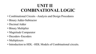
  • 1. UNIT II COMBINATIONAL LOGIC • Combinational Circuits –Analysis and Design Procedures • Binary Adder-Subtractor • Decimal Adder • Binary Multiplier • Magnitude Comparator • Decoders–Encoders • Multiplexers • Introduction to HDL –HDL Models of Combinational circuits.
  • 2. Introduction: • When logic gates are connected together to produce a specified output for certain specified combinations of input variables, with no storage involved, the resulting circuit is called combinational logic circuit. • In combinational logic circuit, the output variables are at all times dependent on the combination of input variables. • The combinational circuit do not use any memory. The previous state of input does not have any effect on the present state of the circuit. • A combinational circuit can have an n number of inputs and m number of outputs.
  • 3. Analysis Procedure Steps to analyse combinational circuit: 1. First make sure that the given circuit is combinational circuit and not the sequential circuit. The combinational circuit has logic gates with no feedback path or memory elements. 2. Label all gate outputs that are a function of input variables with arbitrary symbols and determine the Boolean functions for each gate output. 3. Label the gates that are a function of input variables and previously labelled gates and determine the Boolean functions for them. 4. Repeat the step 3 until the Boolean function for outputs of the circuit are obtained. 5. Finally, substituting previously defined Boolean functions, obtain the output Boolean functions in terms of input variables.
  • 4. 1. Analyze the following logic diagram. Solution: 𝑇1 = 𝐴 𝑇2 = BC 𝑇3 = 𝑇1. 𝑇5 = 𝐴. 𝐴. 𝐷 = 𝐴. 𝐴 + 𝐷 = 𝐴𝐷 𝑇4 = 𝑇1 + 𝐵𝐶 = 𝐴 + 𝐵𝐶 𝑇5 = 𝐴. 𝐷 = 𝐴 + 𝐷 𝐹 = 𝑇3. 𝑇4 = 𝐴𝐷 . 𝐴 + 𝐵𝐶 = 𝐴𝐷 + 𝐴𝐵𝐶𝐷 = 𝐴𝐷 1 + 𝐵𝐶 = 𝐴𝐷 𝐺 = 𝑇4. 𝑇5 = 𝐴 + 𝐵𝐶 . 𝐴 + 𝐷 = 𝐴A + 𝐴𝐷 + 𝐴𝐵𝐶 + 𝐵𝐶𝐷
  • 5. A B C D 𝑻𝟏 𝑻𝟐 𝑻𝟑 𝑻𝟒 𝑻𝟓 F G 0 0 0 0 1 0 1 1 1 1 1 0 0 0 1 1 0 0 1 0 0 0 0 0 1 0 1 0 1 1 1 1 1 0 0 1 1 1 0 0 1 0 0 0 0 1 0 0 1 0 1 1 1 1 1 0 1 0 1 1 0 0 1 0 0 0 0 1 1 0 1 1 1 1 1 1 1 0 1 1 1 1 1 0 1 0 0 0 1 0 0 0 0 0 0 0 1 0 0 1 0 0 1 0 0 0 0 1 0 0 1 0 1 0 0 0 0 0 1 0 0 1 0 1 1 0 0 0 0 1 0 0 1 1 0 0 0 0 0 0 1 0 0 1 1 0 1 0 0 0 0 1 0 0 1 1 1 0 0 1 0 0 1 0 1 1 1 1 1 0 1 0 0 1 0 1 Truth Table 𝐴𝐷 K-Map for output F: 𝐴𝐷 𝐴𝐵𝐶 K-Map for output G:
  • 6. 2. Consider the combinational circuit shown. i)Derive the Boolean expressions for 𝑇1 through 𝑇4.Evaluate the outputs 𝐹1and 𝐹2as a function of the four inputs. ii)List the truth table with 16 binary combinations of the four input variables. Then list the binary values for 𝑇1 through 𝑇4and the outputs 𝐹1and 𝐹2 in the table. iii)Plot the output Boolean function obtained in part (ii) on maps and show the simplified Boolean expressions are equivalent to the ones obtained in part (i).
  • 7. Solution: • 𝑇1 = 𝐵𝐶 • 𝑇2 = 𝐴𝐵 • 𝑇3 = A + 𝐵C • 𝑇4 = AD + 𝐵D + 𝐴B𝐷 • 𝐹1 = A + B𝐷 + 𝐵C + 𝐵D • 𝐹2 = 𝐴B + D A B C D 𝑻𝟏 𝑻𝟐 𝑻𝟑 𝑻𝟒 𝑭𝟏 𝑭𝟐 0 0 0 0 0 0 0 0 0 0 0 0 0 1 0 0 0 1 1 1 0 0 1 0 1 0 1 0 1 0 0 0 1 1 1 0 1 1 1 1 0 1 0 0 0 1 0 1 1 1 0 1 0 1 0 1 0 0 0 1 0 1 1 0 0 1 0 1 1 1 0 1 1 1 0 1 0 0 0 1 1 0 0 0 0 0 1 0 1 0 1 0 0 1 0 0 1 1 1 1 1 0 1 0 1 0 1 0 1 0 1 0 1 1 1 0 1 1 1 1 1 1 0 0 0 0 1 0 1 0 1 1 0 1 0 0 1 1 1 1 1 1 1 0 0 0 1 0 1 0 1 1 1 1 0 0 1 1 1 1 Truth Table
  • 8. K-Map for output 𝑭𝟏: K-Map for output 𝑭𝟐:
  • 9. Design Procedure Steps to design the combinational circuit 1. The problem definition 2. The determination of number of available input variables and required output variables. 3. Assigning letter symbols to input and output variables 4. The derivation of truth table indicating the relationships between input and output variables 5. Obtain simplified Boolean expression for each output 6. Obtain the logic diagram
  • 10. (i) Explain the design procedure of a combinational circuit. (ii)The inputs to a circuit are the 4 bits of the binary number D3D2D1D0.The circuit produces a 1 if and only if all of the following conditions hold 1)MSB is ‘1’or any of the other bits are a ‘0’ 2) D2 is a 1 or any of the other bits are a ‘0’. 3)Any of the 4 bits are 0 Obtain a minimal expression for the output Inputs Output D3 D2 D1 D0 Y 0 0 0 0 1 0 0 0 1 1 0 0 1 0 1 0 0 1 1 1 0 1 0 0 1 0 1 0 1 1 0 1 1 0 1 0 1 1 1 0 1 0 0 0 1 1 0 0 1 1 1 0 1 0 1 1 0 1 1 0 1 1 0 0 1 1 1 0 1 1 1 1 1 0 1 1 1 1 1 0 Truth Table D1D0 D3 D2 D1 D0 00 D1D0 01 D1D0 11 D1D0 10 00 D3 D2 0 1 3 2 01 D3D2 4 5 7 6 11 D3D2 12 13 15 14 10 D3D2 8 9 11 10
  • 11. A majority gate is a digital circuit whose output is equal to 1 if the majority of inputs are 1’s. The output is 0 otherwise. Using a truth table, find the Boolean function implemented by a 3-input majority gate. Simplify the function and implement with gates. Solution: Step 1:Derive the truth table Step 2: Obtain the simplified Boolean expression Step 3: Draw the logic diagram A B C Y 0 0 0 0 0 0 1 0 0 1 0 0 0 1 1 1 1 0 0 0 1 0 1 1 1 1 0 1 1 1 1 1 BC A 00 𝐵 𝐶 01 𝐵 C 11 BC 10 B𝐶 0 𝐴 0 1 3 2 1 A 4 5 7 6
  • 12. Binary Adder Subtractor Adders: • The most basic operation, is the addition of two binary digits. • The simple addition consists of four possible elementary operations, namely, 0+0=0 0+1=1 1+0=1 1+1= 102 • The first three operations produce a sum whose length is one digit, but when the last operation is performed sum is two digits. The higher significant bit of this result is called a carry, and lower significant bit is called sum. • The logic circuit which performs this operation is called a half-adder. • The circuit which performs addition of three bits is called a full-adder.
  • 13. 11. Design a half adder and full adder. Two binary inputs: augend and addend bits Two binary outputs: sum and carry K-map simplification: Logic diagram: Inputs Outputs A B Carry Sum 0 0 0 0 0 1 0 1 1 0 0 1 1 1 1 0 Truth Table for half adder Block schematic of half adder B A 0 𝐵 1 B 0 𝐴 0 0 1 A 0 1 B A 0 𝐵 1 B 0 𝐴 0 1 1 A 1 0 Carry Sum Carry=AB Sum=A𝐵 +𝐴𝐵 =A + B
  • 14. Full Adder • A full adder is a combinational circuit that forms the arithmetic sum of three input bits. • It consist of three inputs and two outputs. • Two of the input variables, denoted by A and B, represent the two significant bits to be added. The third input Cin, represents the carry from the previous lower significant position. Full adder A B Cin Cout Sum Block Schematic of full adder
  • 15. Inputs Outputs A B Cin Carry (Cout) Sum 0 0 0 0 0 0 0 1 0 1 0 1 0 0 1 0 1 1 1 0 1 0 0 0 1 1 0 1 1 0 1 1 0 1 0 1 1 1 1 1 Truth table of full adder K-map simplification for carry and sum BCin A 00 𝐵 Cin 01 𝐵Cin 11 BCin 10 BCin 0 𝐴 0 0 0 1 1 3 0 2 1 A 0 4 1 5 1 7 1 6 BCin A 00 𝐵 Cin 01 𝐵Cin 11 BCin 10 BCin 0 𝐴 0 0 1 1 0 3 1 2 1 A 1 4 0 5 1 7 0 6 K-map for Carry (Cout ) K-map for Sum 𝑪𝒐𝒖𝒕 = 𝑨𝑩 + 𝑨𝑪𝒊𝒏 + 𝑩𝑪𝒊𝒏 𝑺𝒖𝒎 = 𝑨𝑩𝑪𝒊𝒏 + 𝑨𝑩𝑪𝒊𝒏+ 𝐀𝑩𝑪𝒊𝒏 + 𝐀𝐁𝑪𝒊𝒏
  • 16. Implementation using logic gates: 𝑺𝒖𝒎 = 𝑨𝑩𝑪𝒊𝒏 + 𝑨𝑩𝑪𝒊𝒏+ 𝐀𝑩𝑪𝒊𝒏 + 𝐀𝐁𝑪𝒊𝒏 = 𝑪𝒊𝒏(𝑨𝑩 + 𝐀𝐁) + 𝑪𝒊𝒏(𝑨𝑩+ 𝐀𝑩) = 𝑪𝒊𝒏(𝑨ʘ𝑩) + 𝑪𝒊𝒏(𝑨⨁𝑩) = 𝑪𝒊𝒏(𝑨⨁𝑩) + 𝑪𝒊𝒏(𝑨⨁𝑩) 𝑺𝒖𝒎 = 𝑪𝒊𝒏⨁(𝑨⨁𝑩)
  • 17. Full adder using two half adders: 𝑪𝒐𝒖𝒕 = 𝑨𝑩 + 𝑨𝑪𝒊𝒏 + 𝑩𝑪𝒊𝒏 = 𝑨𝑩 + 𝑨𝑪𝒊𝒏 𝑩 + 𝑩 + 𝑩𝑪𝒊𝒏 𝑨 + 𝑨 = 𝑨𝑩 + (𝑨𝑩𝑪𝒊𝒏 + 𝑨𝑩𝑪𝒊𝒏) + 𝑨𝑩𝑪𝒊𝒏 + 𝑨𝑩𝑪𝒊𝒏 = 𝑨𝑩 𝟏 + 𝑪𝒊𝒏 + 𝑪𝒊𝒏 + 𝑨𝑩𝑪𝒊𝒏 + 𝑨𝑩𝑪𝒊𝒏 = 𝑨𝑩 + 𝑨𝑩𝑪𝒊𝒏 + 𝑨𝑩𝑪𝒊𝒏 = 𝑨𝑩 + 𝑪𝒊𝒏 𝑨𝑩 + 𝑨𝑩 𝑪𝒐𝒖𝒕 = 𝑨𝑩 + 𝑪𝒊𝒏 𝑨⨁𝑩 𝑺𝒖𝒎 = 𝑪𝒊𝒏⨁(𝑨⨁𝑩)
  • 18. Subtractors: • The subtraction consists of four possible elementary operations, namely, 0-0=0 0-1=1 with 1 borrow 1-0=1 1-1= 0 • In all operations, each subtrahend bit is subtracted from the minuend bit. • In case of second operation the minuend bit is smaller than the subtrahend bit, hence 1 is borrowed. Half Subtractor: A half-subtractor is a combinational circuit that subtracts two bits and produces their difference. It also has an output to specify if a 1 has been borrowed.
  • 19. K-map simplification: Logic diagram: Inputs Outputs A B Difference Borrow 0 0 0 0 0 1 1 1 1 0 1 0 1 1 0 0 Truth Table for half subtractor B A 0 𝐵 1 B 0 𝐴 0 1 1 A 0 0 B A 0 𝐵 1 B 0 𝐴 0 1 1 A 1 0 Borrow Difference Borrow=𝐴B Difference=A𝐵 +𝐴𝐵 =A + B Limitations: In multidigit subtraction, we have to add two bits along with the borrow of previous digit subtraction. Effectively such subtraction requires subtraction of three bits. This is not possible with half subtractor.
  • 20. Full Subtractor • A half-subtractor is a combinational circuit that performs a subtraction between two bits taking into account of the lower significant stage. • This circuit has three inputs: A,B and Bin minuend,subtrahend and previous borrow and two outputsD and Bout BBin A 00 𝐵 Bin 01 𝐵Bin 11 BBin 10 BBin 0 𝐴 0 0 1 1 0 3 1 2 1 A 1 4 0 5 1 7 0 6 Inputs Outputs A B Bin D Bout 0 0 0 0 0 0 0 1 1 1 0 1 0 1 1 0 1 1 0 1 1 0 0 1 0 1 0 1 0 0 1 1 0 0 0 1 1 1 1 1 Truth table of full subtractor K-map simplification for Difference,D: 𝑫 = 𝑨𝑩𝑩𝒊𝒏 + 𝑨𝑩𝑩𝒊𝒏+ 𝐀𝑩𝑩𝒊𝒏 + 𝐀𝐁𝑩𝒊𝒏 K-map simplification for Bout : BBin A 00 𝐵 Bin 01 𝐵Bin 11 BBin 10 BBin 0 𝐴 0 0 1 1 1 3 1 2 1 A 0 4 0 5 1 7 0 6 𝑩𝒐𝒖𝒕 = 𝐴𝑩 + 𝐴𝑩𝒊𝒏 + 𝑩𝑩𝒊𝒏
  • 21. Implementation using logic gates: 𝑫𝒊𝒇𝒇𝒆𝒓𝒆𝒏𝒄𝒆, 𝑫 = 𝑨𝑩𝑩𝒊𝒏 + 𝑨𝑩𝑩𝒊𝒏+ 𝐀𝑩𝑩𝒊𝒏 + 𝐀𝐁𝑩𝒊𝒏 = 𝑩𝒊𝒏(𝑨𝑩 + 𝐀𝐁) + 𝑩𝒊𝒏(𝑨𝑩+ 𝐀𝑩) = 𝑩𝒊𝒏(𝑨ʘ𝑩) + 𝑩𝒊𝒏(𝑨⨁𝑩) = 𝑩𝒊𝒏(𝑨⨁𝑩) + 𝑩𝒊𝒏(𝑨⨁𝑩) 𝑫 = 𝑩𝒊𝒏⨁(𝑨⨁𝑩)
  • 22. Full Subtractor using two half subtractor: 𝑩𝒐𝒖𝒕 = 𝐴𝑩 + 𝐴𝑩𝒊𝒏 + 𝑩𝑩𝒊𝒏 = 𝐴𝑩 + 𝐴𝑩𝒊𝒏 𝑩 + 𝑩 + 𝑩𝑩𝒊𝒏 𝑨 + 𝑨 = 𝐴𝑩 + 𝐴𝑩𝑩𝒊𝒏 + 𝐴𝑩𝑩𝒊𝒏 + 𝑨𝑩𝑩𝒊𝒏 + 𝑨𝑩𝑩𝒊𝒏 = 𝐴𝑩 𝟏 + 𝑩𝒊𝒏 + 𝑩𝒊𝒏 + 𝐴𝑩𝑩𝒊𝒏 + 𝑨𝑩𝑩𝒊𝒏 = 𝐴𝑩 + 𝐴𝑩𝑩𝒊𝒏 + 𝑨𝑩𝑩𝒊𝒏 = 𝐴𝑩 + 𝑩𝒊𝒏 𝐴𝑩 + 𝑨𝑩 𝑩𝒐𝒖𝒕 = 𝑨𝑩 + 𝑩𝒊𝒏 𝑨⨁𝑩 𝑫 = 𝑩𝒊𝒏⨁(𝑨⨁𝑩)
  • 23. Parallel Adder: • In order to add binary numbers with more than one bit, additional full adders must be employed. • A n-bit parallel adder can be constructed using number of full adder circuits connected in parallel. • The n-bit parallel adder is built using number of full adder circuits connected in cascade, i.e., the carry output of each adder is connected to the carry input of the next higher-order adder. • It should be noted that either a half-adder can be used for the least significant position or the carry input of a full-adder is made 0 because there is no carry into the least significant bit position.
  • 24. Design a 4-bit parallel adder using full-adders. Here, for least significant position, carry input of full adder is made 0.
  • 25. Parallel Subtractor • The subtraction of binary numbers can be done most conveniently by means of complements. • The subtraction A-B can be done by taking the 2’s complement of B and adding it to A. • The 2’s complement can be obtained by taking the 1’s complement and adding one to the least significant pair of bits. • The 1’s complement can be implemented with inverters and a one can be added to the sum through the input carry.
  • 26. Parallel Adder/Subtractor: • The operations of both addition and subtraction can be performed by a one common binary adder. • Such binary circuit can be designed by adding an Ex-OR gate with each full adder. • The mode input control line M is connected with carry input of the least significant bit of the full adder. • This control line decides the type of operation, whether addition or subtraction.
  • 27. • When M= 1, the circuit is a subtractor and when M=0, the circuit becomes adder. • The Ex-OR gate consists of two inputs to which one is connected to the B and other to input M. • When M = 0, B Ex-OR of 0 produce B. • Then full adders add the B with A with carry input zero and hence an addition operation is performed. • When M = 1, B Ex-OR of 1 produce B complement and also carry input is 1. • Hence the complemented B inputs are added to A and 1 is added through the input carry, nothing but a 2’s complement operation. • Therefore, the subtraction operation is performed. • The parallel adder is ripple carry adder in which the carry output of each full-adder stage is connected to the carry input of the next higher order stage. Therefore, the sum and carry outputs of any stage cannot be produced until the input carry occurs; this leads to a time delay in the addition process. This delay is known as carry-propagation delay. • The method of speeding up the process of parallel adder by eliminating inter stage carry delay is called look ahead-carry addition. This method utilizes logic gates to look at the lower-order bits of the augend and addend to see if a higher-order carry is to be generated.
  • 28. Look-Ahead Carry adder • It uses two functions : carry generate and carry propagate Pi=AiꚚBi Gi= AiBi • The output sum and carry can be expressed as, Si=Pi Ꚛ Ci Ci+1=Gi + Pi Ci • Gi is called a carry generate and it produces on carry when both Ai and Bi are one, regardless of the input carry. • Pi is called a carry propagate because it is the term associated with the propagation of the carry from Ci to Ci+1
  • 29. • Now the Boolean function for the carry output of each stage can be written as follows. Ci+1=Gi + Pi Ci C2=G1 + P1 C1 C3=G2 + P2 C2 =G2 + P2 (G1 + P1 C1) =G2 + P2 G1 + P2P1 C1 C4=G3 + P3 C3 =G3 + P3 (G2 + P2 G1 + P2P1 C1) =G3 + P3G2 + P3P2 G1 + P3P2P1 C1 From the above Boolean function it can be seen that C4 does not have to wait for C3 and C2 to propagate; in fact C4 is propagated at the same time as C2 and C3
  • 30.
  • 31. Serial Adder • We can add numbers stored in the right shift registers A and B, serially. • The full-adder is used to perform bit by bit addition and D-flipflop is used to store the carry output generated after addition. • This carry is used as carry input for the next addition. • Initially, the D-flipflop is cleared and addition starts with the least significant bits of both register. • After each clock pulse data within the right shift registers are shifted right 1-bit and we get bits from next digit and carry of previous addition as new inputs for the full adder. • The result SUM is stored bit by bit in the register A. • We can implement serial subtractor by replacing full subtractor instead of full adder and thereby we get difference and borrow instead of sum and carry.
  • 32. Comparison between serial and parallel adder Serial adder Parallel adder • Uses shift register • Uses registers with parallel load capacity • Requires only one full adder circuit • Number of full adder circuit equal to the number of bits in the binary number • It is a sequential circuit • Purely a combinational circuit • Time required depends on number of bits • Time required does not depend on number of bits • It is slower • It is faster
  • 33. BCD Adder • A BCD adder is a circuit that adds two BCD digits and produces a sum digit also in BCD. • To implement BCD adder we require: 4-bit binary adder for initial addition Logic circuit to detect sum greater than 9 One more 4-bit adder to add 01102 in the sum if the sum is greater than 9 or carry is 1 The logic circuit to detect sum greater than 9 can be simplified by Boolean expression of given truth table. • Y=1 indicates sum is greater than 9. • We can put one more term, Cout in the above expression to check whether carry is one. • If any one condition is satisfied we add 6(0110) in the sum. Inputs Outputs S3 S2 S1 S0 Y 0 0 0 0 0 0 0 0 1 0 0 0 1 0 0 0 0 1 1 0 0 1 0 0 0 0 1 0 1 0 0 1 1 0 0 0 1 1 1 0 1 0 0 0 0 1 0 0 1 0 1 0 1 0 1 1 0 1 1 1 1 1 0 0 1 1 1 0 1 1 1 1 1 0 1 1 1 1 1 1 Truth Table
  • 34. S1S0 S3 S2 S1 S0 00 S1S0 01 S1S0 11 S1S0 10 00 S3 S2 0 0 0 1 0 3 0 2 01 S3S2 0 4 0 5 0 7 0 6 11 S3S2 1 12 113 1 15 1 14 10 S3S2 0 8 0 9 1 11 1 10 𝒀 = 𝑺𝟑𝑺𝟐 + 𝑺𝟑𝑺𝟏 K-map Simplification Block diagram of BCD adder • The two BCD numbers, together with input carry, are first added in the top 4-bit binary adder to produce a binary sum. • When the output carry is equal to zero (i.e., when sum ≤ 9 and Cout =0) nothing (zero) is added to the binary sum. • When the output carry is equal to one (i.e., when sum > 9 and Cout =1) binary 0110 is added to the binary sum through the bottom 4-bit binary adder. • The output carry generated from the bottom binary adder can be ignored, since it supplies information already available at the output-carry terminal.
  • 35. Design an 8-bit BCD adder using 4-bit binary adder.
  • 36. BCD Subtractor Subtractor using 9’s Complement method: • The steps for 9’s complement BCD subtraction is as follows: • Find the 9’s complement of the negative number  it is done by inverting each bit of BCD number and adding 10(1010) to it. • Add two numbers using BCD addition • If carry is generated add carry to the result otherwise find the 9’s complement of the result.
  • 37.
  • 38. Subtractor using 10’s Complement method: The steps for 10’s complement BCD subtraction is as follows: • Find the 10’s complement of the negative number  (9’s complement+1) • Add two numbers using BCD addition • If carry is not generated find the 10’s complement of the result.
  • 39.
  • 40. Binary Multiplier: • The multiplication process for binary numbers is similar to the decimal numbers. • Actually binary multiplication is simple than decimal multiplication since it involves only 1s and 0s. • Rules for binary multiplication: • 0*0=0 • 0*1=0 • 1*0=0 • 1*1=1 • The combinational logic circuit implemented to perform such multiplication is called combinational multiplier or array multiplier. 2 x 2 Multiplier: Two unsigned 2-bit numbers: Multiplicand,A= 𝐴1𝐴0 and multiplier B= 𝐵1 𝐵0 The multiplication process involves multiplication(product) of 2-bit number and addition of 2-bit number. The multiplication of 2-bits can be implemented using 2-input AND gate whereas addition of 2-bits can be implemented using half-adder.
  • 41. 𝐴1 𝐴0 X 𝐵1 𝐵0 𝐵0𝐴1 𝐵0𝐴0 + 𝐵1𝐴1 𝐵1𝐴0 𝑃3 𝑃2 𝑃1 𝑃0 Multiplication Process 𝑃0= 𝐵0𝐴0 𝑃1=𝐵0𝐴1+ 𝐵1𝐴0 𝑃2= 𝐵1𝐴1 + carry output of 𝑃1 𝑃3= carry output of 𝑃2 2 x 2 bit combinational array multiplier
  • 42. 4 x 4 multiplier: 𝐴3 𝐴2 𝐴1 𝐴0 x 𝐵3 𝐵2 𝐵1 𝐵0 𝐵0𝐴3 𝐵0𝐴2 𝐵0𝐴1 𝐵0𝐴0 𝐵1𝐴3 𝐵1𝐴2 𝐵1𝐴1 𝐵1𝐴0 𝐵2𝐴3 𝐵2𝐴2 𝐵2𝐴1 𝐵2𝐴0 + 𝐵3𝐴3 𝐵3𝐴2 𝐵3𝐴1 𝐵3𝐴0 𝑃7 𝑃6 𝑃5 𝑃4 𝑃3 𝑃2 𝑃1 𝑃0
  • 43. Design a multiple circuit to multiply the following binary number A=A0A1A2 and B=B0B1B2B3
  • 44. Magnitude comparator • A comparator is a special combinational circuit designed primarily to compare the relative magnitude of two binary numbers. • The n-bit comparator receives two n-bit numbers A and B as inputs and outputs are A>B, A=B and A<B. • Depending upon the relative magnitudes of the two number, one of the outputs will be high.
  • 45. Design a 1-bit comparator using basic gates. Solution: Inputs Outputs A B 𝒀𝑨=𝑩 𝒀𝑨>𝑩 𝒀𝑨<𝑩 0 0 1 0 0 0 1 0 0 1 1 0 0 1 0 1 1 1 0 0 B A 0 𝐵 1 B 0 𝐴 1 0 1 A 0 1 B A 0 𝐵 1 B 0 𝐴 0 0 1 A 1 0 B A 0 𝐵 1 B 0 𝐴 0 1 1 A 0 0 𝒀𝑨=𝑩 𝒀𝑨>𝑩 𝒀𝑨<𝑩 𝒀𝑨=𝑩 = 𝑨𝑩 + 𝑨𝑩 = 𝐴 ⊕ 𝐵 =AʘB 𝒀𝑨>𝑩 = 𝑨𝑩 𝒀𝑨<𝑩 = 𝑨𝑩
  • 46. Design 2-bit comparator using gates. Inputs Outputs 𝑨𝟏 𝑨𝟎 𝑩𝟏 𝑩𝟎 A>B A=B A<B 0 0 0 0 0 1 0 0 0 0 1 0 0 1 0 0 1 0 0 0 1 0 0 1 1 0 0 1 0 1 0 0 1 0 0 0 1 0 1 0 1 0 0 1 1 0 0 0 1 0 1 1 1 0 0 1 1 0 0 0 1 0 0 1 0 0 1 1 0 0 1 0 1 0 0 1 0 1 0 1 1 0 0 1 1 1 0 0 1 0 0 1 1 0 1 1 0 0 1 1 1 0 1 0 0 1 1 1 1 0 1 0 Truth table: K-map Simplification: B1B0 A1 A0 B1 B0 00 B1B0 01 B1B0 11 B1B0 10 00 A1 A0 0 1 3 2 01 A1A0 4 5 7 6 11 A1A0 12 13 15 14 10 A1A0 8 9 11 10
  • 47.
  • 48. Code Conversion Design a 4-bit binary to BCD converter. Step 1: Truth Table for the code converter Step 2: K-map simplification for each BCD output 𝑫𝟎=𝑩𝟎 𝑫𝟏 = 𝑩𝟑𝑩𝟐𝑩𝟏 + 𝑩𝟑 𝑩𝟏 𝑫𝟐 = 𝑩𝟑𝑩𝟐 + 𝑩𝟐 𝑩𝟏 𝑫𝟑 = 𝑩𝟑𝑩𝟐 𝑩𝟏 𝑫𝟒 = 𝑩𝟑𝑩𝟐 + 𝑩𝟑𝑩𝟏 Binary code BCD code 𝑩𝟑 𝑩𝟐 𝑩𝟏 𝑩𝟎 𝑫𝟒 𝑫𝟑 𝑫𝟐 𝑫𝟏 𝑫𝟎 0 0 0 0 0 0 0 0 0 0 0 0 1 0 0 0 0 1 0 0 1 0 0 0 0 1 0 0 0 1 1 0 0 0 1 1 0 1 0 0 0 0 1 0 0 0 1 0 1 0 0 1 0 1 0 1 1 0 0 0 1 1 0 0 1 1 1 0 0 1 1 1 1 0 0 0 0 1 0 0 0 1 0 0 1 0 1 0 0 1 1 0 1 0 1 0 0 0 0 1 0 1 1 1 0 0 0 1 1 1 0 0 1 0 0 1 0 1 1 0 1 1 0 0 1 1 1 1 1 0 1 0 1 0 0 1 1 1 1 1 0 1 0 1
  • 49.
  • 50. Design a logic circuit to convert BCD to gray code. BCD code Gray code 𝑫𝟑 𝑫𝟐 𝑫𝟏 𝑫𝟎 𝑮𝟑 𝑮𝟐 𝑮𝟏 𝑮𝟎 0 0 0 0 0 0 0 0 0 0 0 1 0 0 0 1 0 0 1 0 0 0 1 1 0 0 1 1 0 0 1 0 0 1 0 0 0 1 1 0 0 1 0 1 0 1 1 1 0 1 1 0 0 1 0 1 0 1 1 1 0 1 0 0 1 0 0 0 1 1 0 0 1 0 0 1 1 1 0 1 Step 1: Truth Table for the code converter Step 2: K-map simplification for each Gray output 𝑮𝟎=𝑫𝟏⨁𝑫𝟎 𝑮𝟏 = 𝑫𝟐⨁𝑫𝟏 𝑮𝟐=𝑫𝟐 + 𝑫𝟑 𝑮𝟑=𝑫𝟑 Logic diagram:
  • 51. 1. Design a logic circuit to convert the 8421 BCD to Excess-3 code. 2. Design and implement a 8421 to gray code converter. Realize using NAND gates only. 3. Design a gray to BCD code converter.
  • 52. Decoders • A decoder is a multiple-input, multiple-output logic circuit which converts coded inputs into coded outputs, where the input and output codes are different. • The encoded information is presented as n inputs producing 2n possible outputs. • The 2n output values are from 0 to 2n -1. • Usually, a decoder is provided with enable inputs to activate decoded output based on data inputs. When any one enable input is unasserted, all outputs of decoder are disabled.
  • 53. Binary Decoder • A decoder which has an n-bit binary input code and a one activated output out of 2n output code is called binary decoder. • A binary decoder is used when it is necessary to activate exactly one of 2n outputs based on an n-bit input value. Inputs Outputs EN A B 𝒀𝟑 𝒀𝟐 𝒀𝟏 𝒀𝟎 0 X X 0 0 0 0 1 0 0 0 0 0 1 1 0 1 0 0 1 0 1 1 0 0 1 0 0 1 1 1 1 0 0 0 Truth Table for a 2 to 4 decoder
  • 54. • 2 inputs are decoded into four outputs, each output representing one of the minterms of the 2 input variables. • The two inverters provide the complement of the inputs, and each one of four AND gates generates one of the minterms. • If enable input is 1(EN=1), one, and only one, of the outputs 𝑌0 to 𝑌3, is active for a given input. • The output 𝑌0 is active, i.e. 𝑌0=1 when inputs A=B=0, the output 𝑌1is active when inputs A=0 and B=1. • If enable input is 0, i.e. EN=0, then all the outputs are 0.
  • 55. Draw the circuit for 3 to 8 decoder and explain. • In this, 3 inputs are decoded into eight outputs, each output represent one of the minterms of the 3 input variables. • The three inverters provide the complement of the inputs, and each one of the eight AND gates generates one of the minterms. • Enable input is provided to activate decoded output based on data inputs A,B and C. Inputs Outputs EN A B C 𝒀𝟕 𝒀𝟔 𝒀𝟓 𝒀𝟒 𝒀𝟑 𝒀𝟐 𝒀𝟏 𝒀𝟎 0 X X X 0 0 0 0 0 0 0 0 1 0 0 0 0 0 0 0 0 0 0 1 1 0 0 1 0 0 0 0 0 0 1 0 1 0 1 0 0 0 0 0 0 1 0 0 1 0 1 1 0 0 0 0 1 0 0 0 1 1 0 0 0 0 0 1 0 0 0 0 1 1 0 1 0 0 1 0 0 0 0 0 1 1 1 0 0 1 0 0 0 0 0 0 1 1 1 1 1 0 0 0 0 0 0 0
  • 56. Expanding Cascading Decoders • Binary decoder circuits can be connected together to form a larger decoder circuit. • The figure shows 4x16 decoder using two 3x8 decoder. • Here, one input line (D) is used to enable /disable the decoders. • When D=0, the top decoder is enabled and the other is disabled. • Thus the bottom decoder outputs are all 1s and the top eight outputs generate minterms 0000 to 0111. • When D=1, the enable conditions are reversed and thus bottom decoder outputs generate minterms 1000 to 1111, while the outputs of the top decoder are all 1s.
  • 57. Design 5-to-32 decoder using one 2-to-4 and four 3-to-8 decoder ICs.
  • 58. • Implement the following multiple output combinational logic using a 4 line to 16 line decoder. 𝒀𝟏 = 𝑨𝑩𝑪𝑫 + 𝑨𝑩𝑪𝑫 + 𝑨𝑩𝑪𝑫 + 𝑨𝑩𝑪𝑫 + 𝑨𝑩𝑪𝑫 + 𝑨𝑩𝑪𝑫 𝒀𝟐 = 𝑨𝑩𝑪𝑫 + 𝑨𝑩𝑪𝑫 + 𝑨𝑩𝑪𝑫 + 𝑨𝑩𝑪𝑫 𝒀𝟑 = 𝑨𝑩𝑪𝑫 + 𝑨𝑩𝑪𝑫 + 𝑨𝑩𝑪𝑫
  • 59. • Implement the following multiple output combinational logic function using a 4 line to 16 line decoder. 𝒇𝟏 = 𝜮𝒎 𝟏, 𝟐, 𝟒, 𝟕, 𝟖, 𝟏𝟏, 𝟏𝟐, 𝟏𝟑 ;𝒇𝟐 = 𝜮𝒎 𝟐, 𝟑, 𝟗, 𝟏𝟏 ;𝒇𝟑 = 𝜮𝒎 𝟏𝟎, 𝟏𝟐, 𝟏𝟑, 𝟏𝟒 𝒇𝟒 = 𝜮𝒎 𝟐, 𝟒, 𝟖
  • 60. Design and implement a full adder circuit using a 3:8 decoder. Solution: Truth table of full adder Inputs Outputs A B Cin Carry (Cout) Sum 0 0 0 0 0 0 0 1 0 1 0 1 0 0 1 0 1 1 1 0 1 0 0 0 1 1 0 1 1 0 1 1 0 1 0 1 1 1 1 1
  • 61. Applications of Decoders: • Code converters • Implementation of combinational circuits • Address decoding • BCD to 7-segment decoder Decoder ICs: 3:8 Decoder – 74138 Dual 2:4 Decoder – 74139 BCD to decimal decoder – 7442 BCD to 7-segment decoder – 7447
  • 62. Encoders • An encoders is a digital circuit that performs the inverse operation of a decoder. • An encoder has 2𝑛 (or fewer) input lines and n output lines. • In encoder the output lines generate the binary code corresponding to the input value.
  • 63. Decimal to BCD Encoder • The decimal to BCD encoder, usually has ten input lines and four output lines. • The decoded decimal data acts as an input for encoder and encoded BCD output is available on the four output lines. • In IC 74XX147, it has nine input lines and four output lines, • Both the input and output lines are asserted active low. • It is important to note that there is no input line for decimal zero, when this condition occurs, all output lines are 1.
  • 64. Decimal Value Inputs Outputs 1 2 3 4 5 6 7 8 9 D C B A 0 1 1 1 1 1 1 1 1 1 1 1 1 1 1 0 1 1 1 1 1 1 1 1 1 1 1 0 2 X 0 1 1 1 1 1 1 1 1 1 0 1 3 X X 0 1 1 1 1 1 1 1 1 0 0 4 X X X 0 1 1 1 1 1 1 0 1 1 5 X X X X 0 1 1 1 1 1 0 1 0 6 X X X X X 0 1 1 1 1 0 0 1 7 X X X X X X 0 1 1 1 0 0 0 8 X X X X X X X 0 1 0 1 1 1 9 X X X X X X X X 0 0 1 1 0 X denotes don’t care condition Truth Table for Decimal to BCD encoder
  • 65. Priority Encoder • A priority encoder is an encoder circuit that includes the priority function. • In priority encoder, if two or more inputs are equal to 1 at the same time, the input having the highest priority will take precedence. • 𝐷3 input with highest priority and 𝐷0 input with lowest priority. When 𝐷3 input is high, regardless of other inputs output is 11(𝑌1 𝑌0 = 11) • The 𝐷2 has the next priority. Thus, when 𝐷3=0 and 𝐷2 = 1, regardless of other two lower priority input, output is 10. • The output for 𝐷1 is generated only if higher priority inputs are 0 and so on. • The output V (a valid output indicator) indicates, one or more of the inputs are equal to 1. If all inputs are 0, V is equal to 0, and the other two outputs (𝑌1 and 𝑌0) of the circuit are not used. Inputs Outputs 𝑫𝟎 𝑫𝟏 𝑫𝟐 𝑫𝟑 𝒀𝟏 𝒀𝟎 V 0 0 0 0 X X 0 1 0 0 0 0 0 1 X 1 0 0 0 1 1 X X 1 0 1 0 1 X X X 1 1 1 1 Truth table of 4-bit priority encoder
  • 66. By K-map Simplification: D2D3 D0 D1 00 01 11 10 00 X 0 1 1 1 3 1 2 01 0 4 1 5 1 7 1 6 11 0 12 113 1 15 1 14 10 0 8 1 9 1 11 1 10 D2D3 D0 D1 00 01 11 10 00 X 0 1 1 1 3 0 2 01 1 4 1 5 1 7 0 6 11 1 12 113 1 15 0 14 10 0 8 1 9 1 11 0 10 D2D3 D0 D1 00 01 11 10 00 0 0 1 1 1 3 1 2 01 1 4 1 5 1 7 1 6 11 1 12 113 1 15 1 14 10 1 8 1 9 1 11 1 10 For Y1 For Y0 For V Y1 = D2 +D3 V = D0+ D1 +D2 +D3 Y0 = D3 +D1 D2
  • 67. Octal to Binary Encoder • It has eight inputs, one for each octal digit, and three outputs that generate the corresponding binary code. • In encoders it is assumed that only one input has a value of 1 at any given time; otherwise the circuit is meaningless. • The circuit has one more ambiguity that when all inputs are 0s the outputs are 0s. The zero output can also be generated when D0=1. this ambiguity can be resolved by providing an additional output that specifies the valid condition. Inputs Outputs D0 D1 D2 D3 D4 D5 D6 D7 A B C 1 0 0 0 0 0 0 0 0 0 0 0 1 0 0 0 0 0 0 0 0 1 0 0 1 0 0 0 0 0 0 1 0 0 0 0 1 0 0 0 0 0 1 1 0 0 0 0 1 0 0 0 1 0 0 0 0 0 0 0 1 0 0 1 0 1 0 0 0 0 0 0 1 0 1 1 0 0 0 0 0 0 0 0 1 1 1 1 Encoder ICs: 74147-Decimal to BCD encoder 74148-8-input priority encoder
  • 68. Multiplexers • In digital systems, many times it is necessary to select single data line from several data-input lines, and the data from the selected data line should be available on the output. • This digital circuit which does this task is called a multiplexer. • It is a digital switch. • It allows digital information from several sources to be routed onto a single output line. • The basic multiplexer has several data-input lines and a single output line. • The selection of a particular input line is controlled by a set of selection lines. • Since multiplexer selects one of the input and routes it to output, it is also known as data selector. • Normally, there are 2𝑛 input lines and n selection lines whose bit combinations determine which input is selected. • Therefore, multiplexer is ‘many into one’ and it provides the digital equivalent of an analog selector switch.
  • 69. 2:1 Multiplexer: • D0 is applied as an input to one AND gate and D1 is applied as an input to another AND gate. • Enable input is applied to both gates as one input. • Selection line S is connected as second input to second AND gate. • An inverted S is applied as second input to first AND gate. • Outputs of both AND gates are applied as inputs to OR gate.
  • 70. Working: • When E=0,output is 0,i.e.,Y=0 irrespective of any input condition. • When E=1, the circuit works as follows: a. When S=0, the inverted S, that is gate 1 gets applied as second input to first AND gate. Since S is applied directly as input to second AND gate, its output goes zero irrespective of first input. Since the second input of first AND gate is 1, its output is equal to its first input, that is D0. Hence Y= D0 b. Exactly opposite is the case when S=1. In this case, second AND gate output is equal to its first input D1 and first AND gate output is 0.Hence Y= D1. Enable (E) Select (S) D1 D0 Output Y 1 0 X 0 0 1 0 X 1 1 E𝑆D0 1 1 0 X 0 1 1 1 X 1 ESD1 0 X X X 0 Truth Table for 2:1 multiplexer Y= E𝑆D0 + ESD1
  • 71. 4:1 Multiplexer: E S1 S0 Y 1 0 0 D0 1 0 1 D1 1 1 0 D2 1 1 1 D3 0 X X 0 Function Table
  • 72. 8:1 Multiplexer: S2 S1 S0 Y 0 0 0 D0 0 0 1 D1 0 1 0 D2 0 1 1 D3 1 0 0 D4 1 0 1 D5 1 1 0 D6 1 1 1 D7 (b) Function Table
  • 73. Quadruple 2 to 1 Multiplexer • In some cases, two or more multiplexers are enclosed within one IC package. • The figure shows quadruple 2-to-1 line multiplexer, i.e., four multiplexers, each capable of selecting one of two input lines. E S Output Y 1 X All 0s 0 1 Select A 0 0 Select B Function Table
  • 74. Expanding Multiplexers • It is possible to expand range of inputs for multiplexer beyond the available range by interconnecting several multiplexers in cascade. • The circuit with two or more multiplexers connected to obtain the multiplexer with more number of inputs is known as multiplexer tree. Design 16:1 multiplexer using 8:1 multiplexer.
  • 75. Design 16:1 multiplexer using 4:1 multiplexers.
  • 76. Implementation of combinational logic using MUX 1. Implement the given function using 8:1 multiplexer. F(A,B,C)=Σm(1,3,5,6) Solution: Step 1: Select the multiplexer. Here, Boolean expression has 3 variables, thus we require 23 = 8: 1 multiplexer. Step 2: Connect inputs corresponds to the present minterms to logic 1. Step 3: Connect remaining inputs to logic 0. Step 4: Connect input variables to select lines of MUX.
  • 77. 2. Implement the following Boolean function using 8:1 multiplexer F(A,B,C,D)=𝑨𝑩𝑫 + 𝑨𝑪𝑫 + 𝑩𝑪𝑫 + 𝑨𝑪𝑫 Solution: Step 1:Express the Boolean function in the minterm form. F(A,B,C,D)=Σm(1,3,4,5,6,11,15) Step 2: Implement it using implementation table. D0 D1 D2 D3 D4 D5 D6 D7 𝑨 0 1 2 3 4 5 6 7 A 8 9 10 11 12 13 14 15 0 𝑨 0 1 𝑨 𝑨 𝑨 A Multiplexer Implementation
  • 78. 3. Implement the following Boolean function with 8:1 multiplexer. F(A,B,C,D)=πM(0,3,5,6,8,9,10,12,14) Solution: Here, instead of minterms, maxterms are specified. Thus, we have to circle the maxterms which are not included in the Boolean function. D0 D1 D2 D3 D4 D5 D6 D7 𝑨 0 1 2 3 4 5 6 7 A 8 9 10 11 12 13 14 15 0 𝑨 𝑨 A 𝑨 𝑨 𝟎 1
  • 79. 4. Implement the following Boolean function with 8:1 multiplexer. F(A,B,C,D)=Σm(0,2,6,10,11,12,13)+d(3,8,14) Solution: In the given Boolean function three don’t care conditions are also specified. We know that don’t care conditions can be treated as either 0s or 1s. Here, don’t cares are treated as 1s. D0 D1 D2 D3 D4 D5 D6 D7 𝑨 0 1 2 3 4 5 6 7 A 8 9 10 11 12 13 14 15 1 𝟎 1 1 𝑨 𝑨 𝟏 0
  • 80. 5. Implement full adder circuit using 8:1 multiplexer. Inputs Outputs A B Cin Carry (Cout) Sum 0 0 0 0 0 0 0 1 0 1 0 1 0 0 1 0 1 1 1 0 1 0 0 0 1 1 0 1 1 0 1 1 0 1 0 1 1 1 1 1
  • 81. 6. Implement full adder circuit using quadruple 2 to 1 multiplexer. Solution: Implementation Table Sum: Carry: D0 D1 D2 D3 𝑨 0 1 2 3 A 4 5 6 7 A 𝑨 𝑨 A Inputs Outputs A B Cin Carry (Cout) Sum 0 0 0 0 0 0 0 1 0 1 0 1 0 0 1 0 1 1 1 0 1 0 0 0 1 1 0 1 1 0 1 1 0 1 0 1 1 1 1 1 D0 D1 D2 D3 𝑨 0 1 2 3 A 4 5 6 7 0 𝑨 𝑨 1
  • 82. 7. Realize F(w,x,y,z)=Σ(1,4,6,7,8,9,10,11,15) using 4 to1 MUX. Solution: D0 D1 D2 D3 𝒘𝒙 0 1 2 3 𝒘x 4 5 6 7 w𝒙 8 9 10 11 wx 12 13 14 15 D0=𝑤x+w𝑥 =wꚚx D1=𝑤𝑥+w𝑥 = 𝑥 D2=𝑤x+w𝑥 =wꚚx D3=𝑤x+w𝑥 + 𝑤𝑥 =w+x
  • 83. Applications of Multiplexer: • They are used as a data selector to select one out of many data inputs. • They can be used to implement combinational logic circuit. • They are used in time multiplexing systems. • They are used in frequency multiplexing systems. • They are used in A/D and D/A converter. • They are used in data acquisition systems. Multiplexer ICs: 7415016:1 multiplexer 741518:1 multiplexer 74153Dual 4:1 multiplexer 74157Quad 2-input multiplexer
  • 84. Demultiplexers • A demultiplexer is a circuit that receives information on a single line and transmits this information on one of 2𝑛 possible output lines. • The selection of specific output line is controlled by the values of n selection lines. • It has one input data line, 2𝑛 output lines, n select lines and one enable input.
  • 85. Types of Demultiplexers 1:4 Demultiplexer: • The single input variable Din has a path to all four outputs, but the input information is directed to only one of the output lines depending on the select inputs. • Enable input should be high to enable demultiplexer.
  • 86. 1:8 Demultiplexer: The single input data Din has a path to all eight outputs, but the input information is directed to only one of the output lines depending on the select inputs.
  • 88. Expanding Demultiplexer: To provide larger output needs we can cascade two or more demultiplexer to get demultiplexer with more number of output lines. Such a connection is known as demultiplexer tree. 1. Design 1:8 demultiplexer using two 1:4 demultiplexers. Solution: Step 1: Connect Din signal to Din input of both the demultiplexers. Step 2: Connect select lines B and C to select lines S1 and S0 of the both demultiplexer. Step 3: Connect most significant select line (A) such that when A=0 DEMUX 1 is enabled and when A=1 DEMUX 2 is enabled.
  • 89. Implement 1:16 demultiplexer using 1:4 demultiplexer.
  • 90. Implementation of Combinational Logic using Demultiplexer Implement full subtractor using demultiplexer. Solution: Bout=Σm(1,2,3,7) D=Σm(1,2,4,7) Inputs Outputs A B Bin D Bout 0 0 0 0 0 0 0 1 1 1 0 1 0 1 1 0 1 1 0 1 1 0 0 1 0 1 0 1 0 0 1 1 0 0 0 1 1 1 1 1
  • 91. Implement the following functions using demultiplexer. F1(A,B,C)=Σm(0,3,7) F2(A,B,C)=Σm(1,2,5)
  • 92. Applications of Demultiplexer: • It can be used as a decoder. • It can be used as a data distributor. • It is used in time division multiplexing at the receiving end as a data separator. • It can be used to implement Boolean expression. Demultiplexer ICs: 741541:16 Demultiplexer 74155Dual 1:4 Demultiplexer
  • 93. Introduction to Hardware Description Language Various modeling techniques in HDL  Gate-level modeling/Structural modeling  Dataflow modeling  Behavioral modeling Structure of HDL module • Each module consists of a declaration and a body. • Declaration  name, inputs and outputs of the module are listed. • Body relationship between the inputs and outputs • A module is a basic building block of Verilog HDL. • Modules can represent pieces of hardware ranging from simple gate to complete systems. • The structure of module is, module<module name> <port list>; <declares> <module items> endmodule
  • 94. Operators in Verilog HDL • Boolean logic(!,&&,||) • Unary reduction logical(&, |,^) • Bitwise logical(~&, ~|,~^,~) • Relational(>,>=,<,<=,==,!=) • Binary arithmetic(+,-,*,/,%) • Other (<<,>>)
  • 95. Structure of the Data Flow Description Verilog HDL code for full adder Verilog HDL code for multiplexer with active low enable module full_add (A,B,Cin,Cout,Sum); input A,B,Cin; output Sum,Cout; assign Sum=(A^B) ^Cin; assign Cout=(A & B)|(Cin & A)|(Cin & B); endmodule module mux 2x1(D0,D1,S,Enbar,Y); input D0,D1,S,Enbar; output Y; Wire I1,I2,I3,I4; assign #10 Y=I3|I4; assign #10 I3=D0 & I1 & I2; assign #10 I4=D1 & S & I2; assign #10 I1=~S; assign #10 I2=~Enbar; endmodule
  • 96. Structure of the Behavioral Description Verilog HDL code for full adder Verilog HDL code for multiplexer module full_add (A,B,Cin,Cout,Sum); input A,B,Cin; output Sum,Cout; Reg Sum,Cout; always@(A,B,Cin) begin Sum=(A^B) ^Cin; Cout=(A & B)|(Cin & A)|(Cin & B); end endmodule module mux 2x1(D0,D1,S,Enbar,Y); input D0,D1,S,Enbar; output Y; Reg Y; always@(S,D0,D1,Enbar) begin if(Enbar==0 & S==1) begin Y=D0; end else if(Enbar==0 & S==0) Y=D1; else Y=1’bz; end endmodule
  • 97. Structural/ Gate Level Description Verilog HDL code for full adder Verilog HDL code for multiplexer module full_addER (A,B,Cin,Cout,Sum); input A,B,Cin; output Sum,Cout; Wire S0,C0,C1; full adder HA H1(A,B,S0,C0); HA H2(S0,Cin,Sum,C1); or (Cout,C0,C1) endmodule module HA(A,B,S,C); input A,B; output S,C; xor(S,A,B); and(C,A,B); endmodule module mux 2x1(D0,D1,S,Enbar,Y); input D0,D1,S,Enbar; output Y; and #7 (I3,D0,I1,I2); or #7 (Y,I3,I4); and #7 (I4,D1,S,I2); not #7 (I1,S); not #7 (I2,Enbar); endmodule