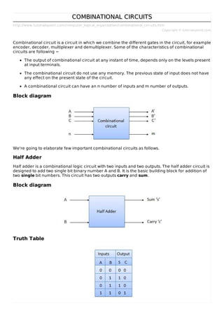
2. Circuit Diagram
Full Adder
Full adder is developed to overcome the drawback of Half Adder circuit. It can add two one-bit
numbers A and B, and carry c. The full adder is a three input and two output combinational circuit.
Block diagram
Truth Table
Circuit Diagram
3. N-Bit Parallel Adder
The Full Adder is capable of adding only two single digit binary number along with a carry input.
But in practical we need to add binary numbers which are much longer than just one bit. To add
two n-bit binary numbers we need to use the n-bit parallel adder. It uses a number of full adders in
cascade. The carry output of the previous full adder is connected to carry input of the next full
adder.
4 Bit Parallel Adder
In the block diagram, A0 and B0 represent the LSB of the four bit words A and B. Hence Full Adder-
0 is the lowest stage. Hence its Cin has been permanently made 0. The rest of the connections are
exactly same as those of n-bit parallel adder is shown in fig. The four bit parallel adder is a very
common logic circuit.
Block diagram
N-Bit Parallel Subtractor
The subtraction can be carried out by taking the 1's or 2's complement of the number to be
subtracted. For example we can perform the subtraction A − B by adding either 1's or 2's
complement of B to A. That means we can use a binary adder to perform the binary subtraction.
4 Bit Parallel Subtractor
The number to be subtracted B is first passed through inverters to obtain its 1's complement. The
4-bit adder then adds A and 2's complement of B to produce the subtraction. S3 S2 S1 S0
represents the result of binary subtraction A − B and carry output Cout represents the polarity of the
result. If A > B then Cout = 0 and the result of binary form A − B then Cout = 1 and the result is in
the 2's complement form.
Block diagram
4. Half Subtractors
Half subtractor is a combination circuit with two inputs and two outputs differenceandborrow. It
produces the difference between the two binary bits at the input and also produces an output
Borrow to indicate if a 1 has been borrowed. In the subtraction A − B, A is called as Minuend bit and B
is called as Subtrahend bit.
Truth Table
Circuit Diagram
Full Subtractors
The disadvantage of a half subtractor is overcome by full subtractor. The full subtractor is a
combinational circuit with three inputs A,B,C and two output D and C'. A is the 'minuend', B is
'subtrahend', C is the 'borrow' produced by the previous stage, D is the difference output and C' is
the borrow output.
Truth Table
5. Circuit Diagram
Multiplexers
Multiplexer is a special type of combinational circuit. There are n-data inputs, one output and m
select inputs with 2m = n. It is a digital circuit which selects one of the n data inputs and routes it to
the output. The selection of one of the n inputs is done by the selected inputs. Depending on the
digital code applied at the selected inputs, one out of n data sources is selected and transmitted to
the single output Y. E is called the strobe or enable input which is useful for the cascading. It is
generally an active low terminal that means it will perform the required operation when it is low.
Block diagram
6. Multiplexers come in multiple variations
2 : 1 multiplexer
4 : 1 multiplexer
16 : 1 multiplexer
32 : 1 multiplexer
Block Diagram
Truth Table
Demultiplexers
A demultiplexer performs the reverse operation of a multiplexer i.e. it receives one input and
distributes it over several outputs. It has only one input, n outputs, m select input. At a time only
one output line is selected by the select lines and the input is transmitted to the selected output
line. A de-multiplexer is equivalent to a single pole multiple way switch as shown in fig.
Demultiplexers comes in multiple variations.
1 : 2 demultiplexer
1 : 4 demultiplexer
1 : 16 demultiplexer
1 : 32 demultiplexer
Block diagram
7. Truth Table
Decoder
A decoder is a combinational circuit. It has n input and to a maximum m = 2n outputs. Decoder is
identical to a demultiplexer without any data input. It performs operations which are exactly
opposite to those of an encoder.
Block diagram
Examples of Decoders are following.
Code converters
BCD to seven segment decoders
Nixie tube decoders
Relay actuator
2 to 4 Line Decoder
The block diagram of 2 to 4 line decoder is shown in the fig. A and B are the two inputs where D
through D are the four outputs. Truth table explains the operations of a decoder. It shows that each
output is 1 for only a specific combination of inputs.
Block diagram
8. Truth Table
Logic Circuit
Encoder
Encoder is a combinational circuit which is designed to perform the inverse operation of the
decoder. An encoder has n number of input lines and m number of output lines. An encoder
produces an m bit binary code corresponding to the digital input number. The encoder accepts an
n input digital word and converts it into an m bit another digital word.
Block diagram
Examples of Encoders are following.
Priority encoders
9. Decimal to BCD encoder
Octal to binary encoder
Hexadecimal to binary encoder
Priority Encoder
This is a special type of encoder. Priority is given to the input lines. If two or more input line are 1 at
the same time, then the input line with highest priority will be considered. There are four input D0,
D1, D2, D3 and two output Y0, Y1. Out of the four input D3 has the highest priority and D0 has the
lowest priority. That means if D3 = 1 then Y1 Y1 = 11 irrespective of the other inputs. Similarly if D3
= 0 and D2 = 1 then Y1 Y0 = 10 irrespective of the other inputs.
Block diagram
Truth Table
Logic Circuit