The document discusses the accumulator register in a CPU. It describes the accumulator as a short-term storage register for arithmetic and logic operations. It contains details about the inputs and outputs to the accumulator from other registers like the data register and input register. It also explains the different microoperations that can be performed on the accumulator like addition, transfer, complement, and shift operations. The control gates for these microoperations are also defined.
An accumulator isa register for short-term,
intermediate storage of arithmetic and logic
data in a computers CPU.
The term “accumulator” is used in reference
to contemporary CPUs, having been
replaced around the turn of the millennium
by the term “register”.
3.
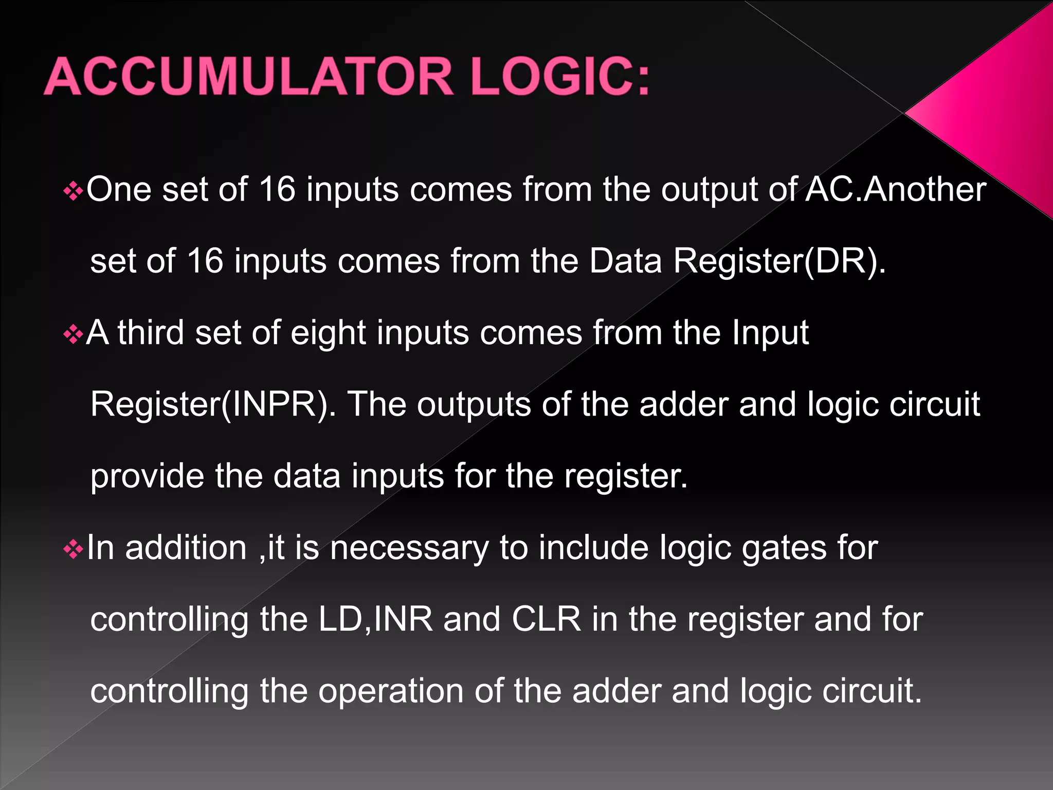
One set of16 inputs comes from the output of AC.Another
set of 16 inputs comes from the Data Register(DR).
A third set of eight inputs comes from the Input
Register(INPR). The outputs of the adder and logic circuit
provide the data inputs for the register.
In addition ,it is necessary to include logic gates for
controlling the LD,INR and CLR in the register and for
controlling the operation of the adder and logic circuit.
4.
D0T5: AC<-AC^DR ANDwith DR
D1T5: AC<-AC+DR Add with DR
D2T5: AC<-DR Transfer from DR
PB11: AC(0-7)<-INPR Transfer from INPR
rB9: AC<-AC Complement
rB7: AC<-shr AC, AC(15)<-E Shift right
rB6: AC<-shr AC, AC(0)<-E Shift left
rB11: AC<-0 clear
rB5: AC<-AC+1 Increment
5.
16 16
8 Tobus
LD INR CLR
Adder and
logic circuit
Accumulator
register(AC)
Control
gates
From DR
From INPR
16
16
6.
The control functionfor the clear microoperation is
rB11,where r=D-I’T3 and B11=IR(11).
The output of the AND gate that genertes this control
functionis connected to the CLR input of the register.
The output of the gate that implements the increment
microoperation is connected to the INR input of the
register.
8.
The other sevenmicrooperations are generated in
the adder and logic circuit and are loaded into AC
at the proper time.
The outputs of the gates for each control function is
marked with a symbolic name.
These outputs are used in the design of the adder and logic
circuit.
9.
The adder andlogic circuit can be subdivided into 16
stages, with each stage corresponding to one bit of AC.
The load(LD) input is connected to the inputs of the
AND gates.
The input is labeled Ii and the output AC(i).When the LD
input is enabled, the 16 inputs Ii for i=0,1,2,...,15 are
transferred to AC(0-15).
The AND operation is achieved by ANDing AC(i) with
the corresponding bit in the data register DR(i).
11.
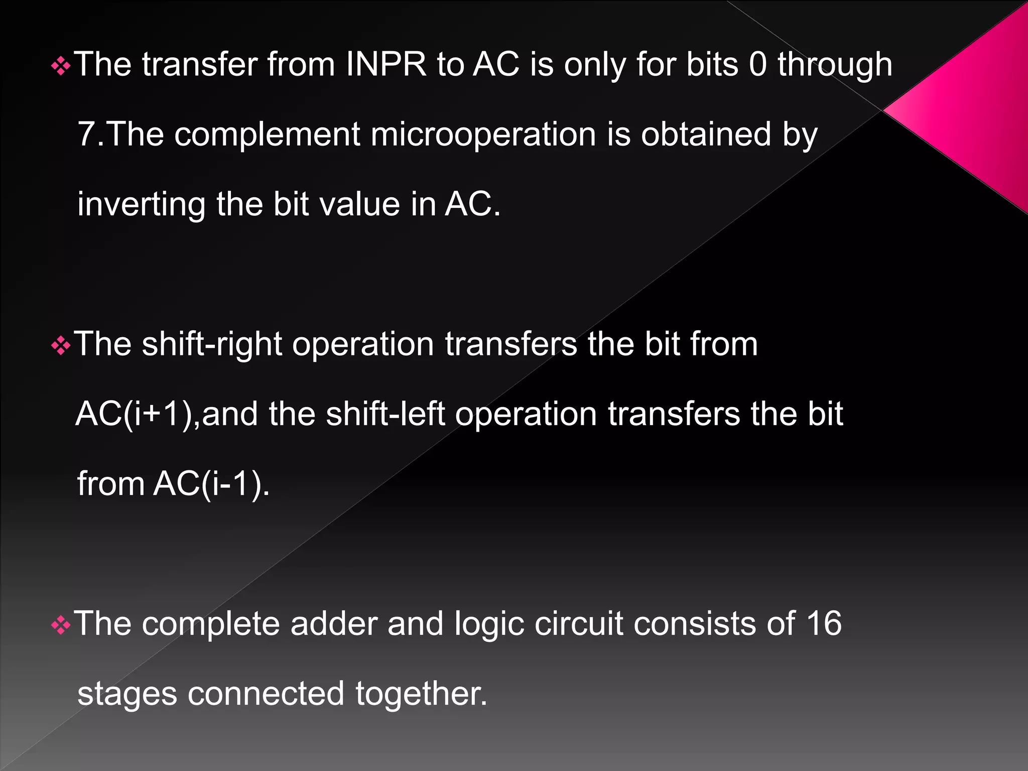
The transfer fromINPR to AC is only for bits 0 through
7.The complement microoperation is obtained by
inverting the bit value in AC.
The shift-right operation transfers the bit from
AC(i+1),and the shift-left operation transfers the bit
from AC(i-1).
The complete adder and logic circuit consists of 16
stages connected together.