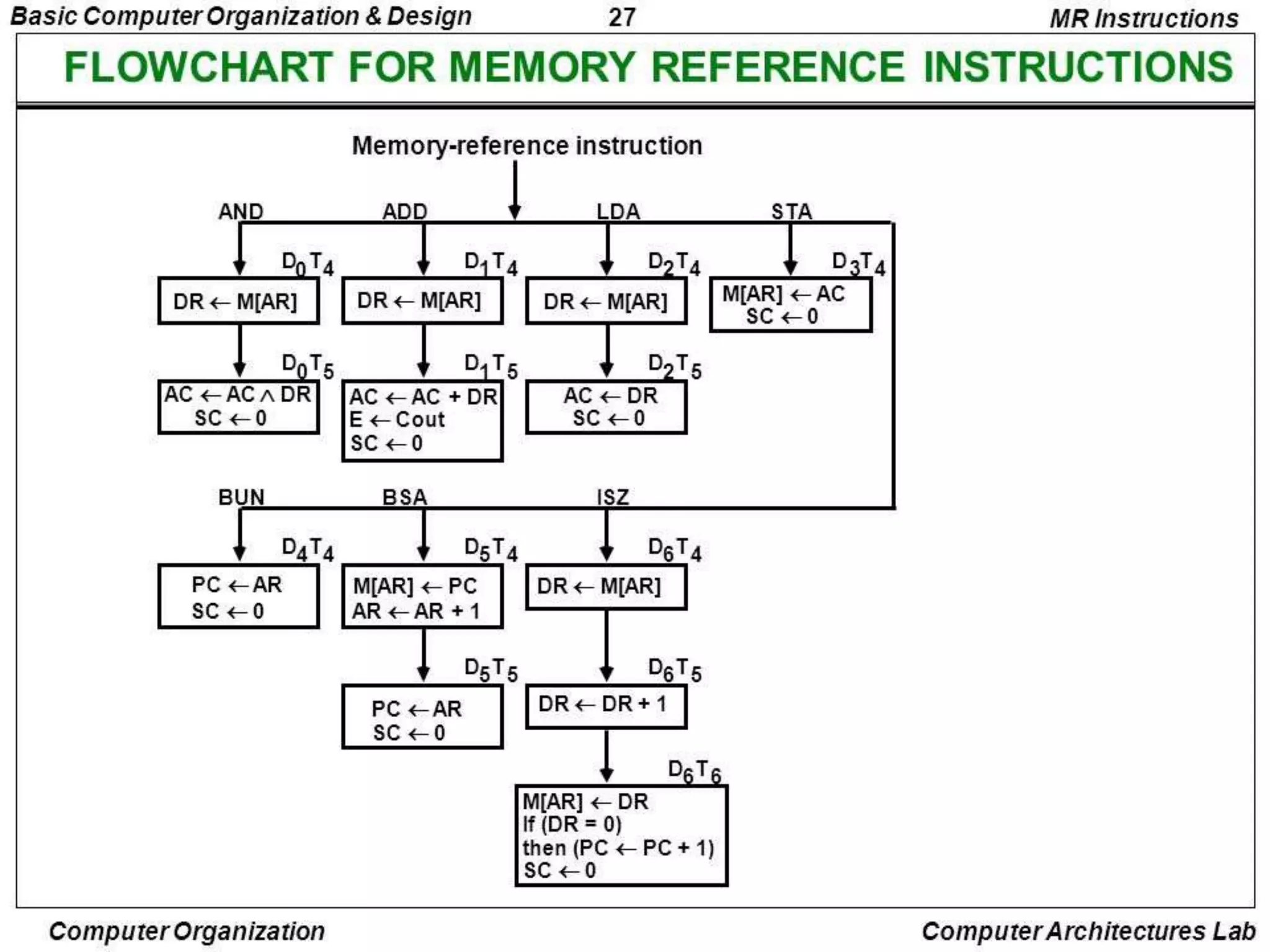
This document discusses memory reference instructions (MRI) and their implementation using microoperations. It defines MRI as instructions that operate on data stored in memory. Seven common MRI are described: AND to AC, ADD to AC, LDA, STA, BUN, BSA, and ISZ. Each MRI is broken down into its constituent microoperations, which are controlled by timing signals. The microoperations transfer data between memory, registers, and logic circuits. A control flow chart illustrates the sequencing of microoperations for each instruction type.

![SYMPOL OPERATION
DECODER
SYMBOLIC DESCRIPTION
AND D0 AC AC ^ M[AR]
ADD D1 AC <- AC+M[AR], E <- Cout
LDA D2 AC <- M[AR]
STA D3 M[AR] <-AC
BUN D4 PC <- AR
BSA D5 M[AR]<- PC, PC<- AR+1
M[AR] <- M[AR]+1
ISZ D6 IF M[AR]+1=0 THEN
PC <- PC+1](https://image.slidesharecdn.com/mri-181001064522/75/memory-reference-instruction-5-2048.jpg)
![AND TO AC:
It performs the AND logic operation in
AC, and the memory word specified by
the “effective address”.
D0T4:DR <- M[AR]
D0T5:AC <-AC ^DR,SC <-0
• The two timing signal are T4 ,T5.
• T4 transfer the operand from memory in
DR.](https://image.slidesharecdn.com/mri-181001064522/75/memory-reference-instruction-6-2048.jpg)
![ADD to AC:
Adds the content of the memory word specified by the
effective addresses.
Sum transferred to AC and output is carry(cout)
transfer to the E flip flop.
D1T4:DR<-M[AR]
D1T5:AC<-AC+DR,E<-COUT,SC<-0
Two timing signals t4 and t5.decoder d1 instead d0
used in AND instruction
Instruction fetched from memory and decoder.](https://image.slidesharecdn.com/mri-181001064522/75/memory-reference-instruction-8-2048.jpg)
![LDA:LOAD to AC:
Memory word specified by the effective addresses to
AC.
D2T4:DR<-M[AR]
D2T5:AC<-DR,SC<-0
No direct path from the bus into AC.
The adder and logic circuit receive information from
DR.transfer to AC.
Read from memory and transfer to the adder and logic
circuit.](https://image.slidesharecdn.com/mri-181001064522/75/memory-reference-instruction-10-2048.jpg)
![STA:-STORE AC:
Memory word specified by the effective address.
Output of AC is applied to the bus data input of
memory is connected to the execute the one
microoperation.
D3T4:M[AR]<-AC,SC<-0.](https://image.slidesharecdn.com/mri-181001064522/75/memory-reference-instruction-11-2048.jpg)
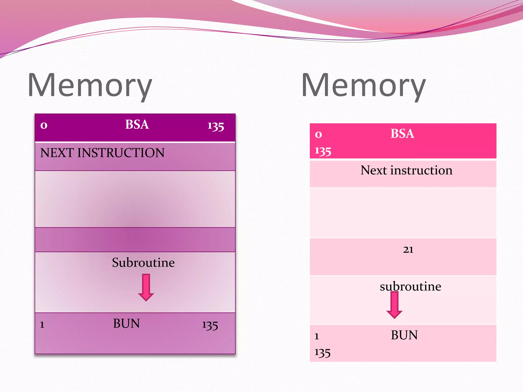
![BSA :-BRANCH and SAVE RETURN
ADDRESS:
Subroutine(or)procedure.
Memory location specified by the effective address.
Address of the first instruction in the subroutine.
M[AR]<-PC, PC<-AR+1.
Next instruction is called return address.
M[135]<-21,PC<-135+1=136.
BSA instruction performs the function usually referred
to as a subroutine call.](https://image.slidesharecdn.com/mri-181001064522/75/memory-reference-instruction-13-2048.jpg)
![ End of the subroutine performs the function refer is called
subroutine return.
D5T4 :M[AR]<-PC,AR <-+1
D5T5 :PC<-AR,SC<-0
Enable the INR input of AR.](https://image.slidesharecdn.com/mri-181001064522/75/memory-reference-instruction-14-2048.jpg)
![ISZ:-INCREMENT and SKIP it ZERO
The instruction increment the word specified by the
effective address.
INR value is 0,PC incremented by 1.
It is stored in a negative number.so used to an 2’s
complements.negative number are incremented by 1.
The instruction is a sequence of microoperation
D6T4:DR<-M[AR].
D6T5: DR<-DR+1.
D6T6:M[AR]<-DR ,if(DR=0)then (PC<-
PC+1),SC<-0.](https://image.slidesharecdn.com/mri-181001064522/75/memory-reference-instruction-16-2048.jpg)