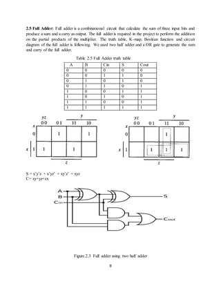
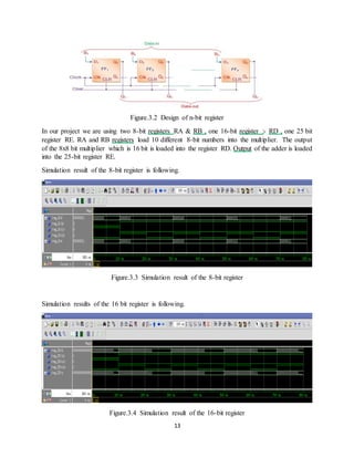
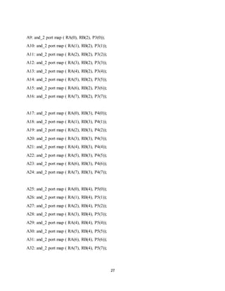
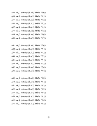
1
PROJECT REPORT
Multiplier Accumulator Circuit
Submitted by:
Daksh Raj Chopra
ID: 40054446
Nitin Singh
ID: 40067571
Rahul Malhotra
ID: 40036643
Submitted to:
Asim J. Al-Khalili
Distinguished Emeritus Professor
Electrical and Computer Engineering
2
TABLE OF CONTENTS
1. INTRODUCTION 5
1.1 Requirements 5
1.2 Project Breakdown 5
2. Combinational Circuits 6
2.1 And Gate 6
2.2 OR Gate 6
2.3 XOR Gate 6
2.4 Half Adder 7
2.5 Full Adder 8
2.6 Multiplier 9
2.7 Ripple carry Adder 11
2.8 Manchester Carry Adder 11
2.9 Multiplexer 11
3. Sequential Circuits 12
3.1 D-Flip Flop 12
3.2 Registers 12
4. Result and simulation 15
4.1 Block Diagram
4.2 Simulation result 16
5. Contribution 17
6. APPENDIX A: VHDL SOURCE 18
3
LIST OF FIGURES
Figure 2.1 Half Adder Circuit 7
Figure 2.2 Simulation result of the half adder 7
Figure 2.3 Full Adder using two half adder 8
Figure 2.4 Simulation result of the full adder 9
Figure 2.5 Multiplier Design using Wallace tree 10
Figure 2.6 Simulation result of the multiplier 10
Figure 2.7 n-bit Ripple Carry Adder 11
Figure 2.8 Simulation result of the 25 bit register 11
Figure 3.1 Circuit diagram of the D-flip flop using Nand and Nor 12
Figure 3.2 Design of n-bit register 13
Figure 3.3 Simulation result of the 8-bit register 13
Figure 3.4 Simulation result of the 16-bit register 13
Figure 3.5 Simulation result of the 25-bit register 14
Figure 4.1 Block Diagram of the Project 15
Figure 4.2 Simulation result of the project 16
4
LIST OF TABLES
Table 2.1 AND gate truth table 6
Table 2.2 OR gate truth table 6
Table 2.3 XOR gate truth table 6
Table 2.4 Half Adder truth table 7
Table 2.5 Full Adder truth table 8
Table 3.1 D-flip flop truth table 12
5
1. Introduction
The objective of this project is to design a multiplier that can calculate the multiplication of two 8
bit numbers and save the result in a 16 bit register. In order to design a multiplier we need 2 8 bit
register, 1 16 bit register. Two input AND gate, A full adder and a half adder. After calculation the
result of 10 consecutive multiplication, that need to save in a accumulator and then addition
perform and save the result in a different register. The goal is to design and simulate the result.
1.1 Requirements: The goal of this project is to design a multiplier accumulator circuit: in 3
stages:
1) Design an 8 bits register. A 16 bits register and a 25 bits register.
8bits of data are arriving on lines A & B in parallel on registers RA and RB. Numbers are
unsigned binary numbers. A total of 10 numbers will arrive in succession on each line. Data
are loaded into registers RA & RB by the command line LOAD.
2) Design a parallel multiplier
Use the parallel multiplier designed to multiply the multiplier (RA) and the multiplicand
(RB). Store the result in register, RD.
3) Design an Adder.
The Adder is used to add the ten results from the multiplier.
The output result will be in register RE.
We need to write the VHDL code, compile it, simulate VHDL design code, test it, synthesize
it.
1.2 Project Breakdown: The design need to be breakdown into a small blocks and start simulate
each block before final simulation of multiplier. The different block of the design is two 8-bit
registers, a multiplier, a 16 bit register, a 25 bit adder and a 25 bit register.
6
2. Combinational Circuits
This chapter includes the combinational circuits we used in the projects. The basic information of
the combinational circuits and simulation results includes in this chapter.
2.1 And Gate: A two input AND gate is required to perform the multiplication of two binary bit.
Here, in the project, we need AND gate in the half adder, full adder and multiplier. The truth table
and Boolean function of an AND gate is given below.
Y= A.B
Table 2.1 AND gate truth table
A B Y
0 0 0
0 1 0
1 0 0
1 1 1
2.2 OR Gate: A two input OR gate is required to perform the function the addition of two binary
bit. We need a two input OR gate in the full adder to get the carry out. The truth table and Boolean
function of a OR gate is given below.
Y=A+B
Table 2.2 OR gate truth table
A B Y
0 0 0
0 1 1
1 0 1
1 1 1
2.3 XOR gate: XOR perform the given Boolean function on the input. We need XOR gate to get
the sum of the half adder. The Boolean function and truth table of a XOR gate is given below.
Y=A’B+ AB’
Table 2.3 XOR gate truth table
A B Y
0 0 0
0 1 1
1 0 1
1 1 0
7
2.4 Half Adder: Half adder is a combinational logic that calculate the sum of two bit and produce
a sum and a carry. It is a basic building block that perform the following Boolean function. We are
using half adder to add some of the partial product that have only two input bits. The truth table,
Boolean function and circuit diagram of the half adder is following.
Sum=A’B+AB’
Carry =A.B
Table 2.4 Half adder truth table
A B Sum Carry
0 0 0 0
0 1 1 0
1 0 1 0
1 1 0 1
The XOR and AND gate are used in the half adder.
Figure.2.1 Half adder Circuit
Simulation result of the half adder is given below:
Figure.2.2 Simulation result of the half adder
8
2.5 Full Adder: Full adder is a combinational circuit that calculate the sum of three input bits and
produce a sum and a carry as output. The full adder is required in the project to perform the addition
on the partial products of the multiplier. The truth table, K-map, Boolean function and circuit
diagram of the full adder is following. We used two half adder and a OR gate to generate the sum
and carry of the full adder.
Table 2.5 Full Adder truth table
S = x’y’z + x’yz’ + xy’z’ + xyz
C= xy+yz+zx
Figure.2.3 Full adder using two half adder
A B Cin S Cout
0 0 0 0 0
0 0 1 1 0
0 1 0 1 0
0 1 1 0 1
1 0 0 1 1
1 0 1 0 1
1 1 0 0 1
1 1 1 1 1
9
Simulation result of the full adder is given below:
Figure.2.4 Simulation result of the full adder
2.6 Multiplier: The requirement of the project is to design a Multiplier that can perform the
multiplication on two 8-bits number.Multiplication of two 8 bits binary number will produce a 16-
bit binary number. Different kind of multiplier cab be used for that such as Add and shift multiplier,
Parallel multiplier, Array multiplier, Wallace tree multiplier. In order to get the optimized design,
we need to see the delay and area. We are considering the delay here and using Wallace tree
multiplier which us fastest multiplier. However, it takes maximum area but timing is more
important factor.
AND gate is being used to generate the partial products.
Number of partial products will be = N*M
Where, N= Length of Multiplicand, M= Length of Multiplier
Here in the project, the length of both multiplicand and multiplier is 8 bit. So, number of partial
products will be 64. The number of AND gates required to calculate the partial products are 64.
A7 A6 A5 A4 A3 A2 A1 A0
X B7 B6 B5 B4 B3 B2 B1 B0
-------------------------------------------------
A7.B0 A6.B0 A5.B0 A4.B0 A3.B0 A2.B0 A1.B0 A0.B0
+ A7.B1 A6.B1 A5.B1 A4.B1 A3.B1 A2.B1 A1.B1 A0.B1
+ A7.B2 A6.B2 A5.B2 A4.B2 A3.B2 A2.B2 A1.B2 A0.B2
+ A7.B3 A6.B3 A5.B3 A4.B3 A3.B3 A2.B3 A1.B3 A0.B3
+ A7.B4 A6.B4 A5.B4 A4.B4 A3.B4 A2.B4 A1.B4 A0.B4
+ A7.B5 A6.B5 A5.B5 A4.B5 A3.B5 A2.B5 A1.B5 A0.B5
+ A7.B6 A6.B6 A5.B6 A4.B6 A3.B6 A2.B6 A1.B6 A0.B6
+A7.B7 A6.B7 A5.B7 A4.B7 A3.B7 A2.B7 A1.B7 A0.B7
----------------------------------------------------------------------------------------
P15 P14 P13 P12 P11 P10 P9 P8 P7 P6 P5 P4 P3 P2 P1 P0
After getting the 64 partial products, we need to add the partial products. There are 48 Full adders
and 8 Half adders used to add the partial products.
Patial
Productsto
be added
10
The area of the multiplier is 64 AND gates, 48 full adders and 8 half adders. The design of the
Wallace tree multiplier is given below. We will get a 16 bit output from the Wallace tree multiplier.
The project requirement is to save this 16 bit binary number into a 16 bit register and further.
Figure.2.5 Multiplier design using Wallace tree
The simulation results of the multiplier is given below:
Figure.2.6 Simulation result of the multiplier
11
2.7 Ripple carry Adder: The Ripple carry adder is designed by cascading full adders in series.
In, project we required a 25 bit adder to add the final outputs of the multiplier. The design of a n-
bit ripple carry adder is given below.
Figure.2.7 n-bit Ripple carry adder
The delay of a n bit adder is n full adder delay. So, 25 bit adder has a 25 full adder delay which is
very large.
The simulation result of the ripple carry adder is given below.
Figure.2.8 Simulation result of 25 bit Ripple carry adder
2.8 Manchester carry Adder: Manchester carry adder has very small delay and useful to reduce
the delay if the circuit. Carry propagate and generate action is taken place initially and go to the
select line of the multiplexer. The half adder is used to propagate and generate. The Boolean
function for propagate and generate is given below.
Gi = Ai Bi --carry generate of ith stage
Pi = Ai Bi --carry propagate of ith stage
Si = Pi Ci --sum of ith stage
Ci+1 = Gi + PiCi --carry out of ith stage
The design of a 16 bit Manchester carry adder is given below. The 25 bit Manchester carry adder
can be constructed by adding cells in series.
2.9 Multiplexer: Mux is a combinational circuit that select one of the input and forward the input
to the output. Select line is used to select the input. A multiplexer 2^n has [n] select lines. Here, to
design the Manchester adder, we need a 2^1 mux. The Select circuit diagram and truth table and
Boolean function of 2^1 mux is given below.
12
3. Sequential Circuits
3.1 D-Flip Flop: D-flip flop is a sequential circuit that is used to get the data from D input and
produce the same date as output with one cycle delay. We are using D flip flop which is also known
as data flip flop or delay flip Flop, to design the 8 bit registers, 16 bit registers and 25 bit registers.
The circuit diagram and the truth table of the D-flip flop is given below.
Figure.3.1 Circuit diagram of D-flip flop using Nand and Nor
Table 3.2 D-flip flop truth table
Q D Q(t+1)
0 0 0
0 1 1
1 0 0
1 1 1
3.2 Registers: Parallel In Parallel Out (PIPO) registers are the type of storage devices in which
both data loading as well as data retrieval processes occur in parallel mode. Figure shows a PIPO
register capable of storing n-bit input data word (Data in). Here each flip-flop stores an individual
bit of the data in appearing as its input (FF1 stores B1 appearing at D1; FF2 stores B2 appearing
at D2 … FFn stores Bn appearing at Dn) at the instant of first clock pulse. Further, at the same
instant, the bit stored in each individual flip-flop also appears at their respective output pins (Q1 =
D1; Q2 = D2 … Qn = Bn). This indicates that both data storage as well as data recovery occur at
a single (and at the same) clock pulse in PIPO registers.
13
Figure.3.2 Design of n-bit register
In our project we are using two 8-bit registers RA & RB , one 16-bit register :- RD , one 25 bit
register RE. RA and RB registers load 10 different 8-bit numbers into the multiplier. The output
of the 8x8 bit multiplier which is 16 bit is loaded into the register RD. Output of the adder is loaded
into the 25-bit register RE.
Simulation result of the 8-bit register is following.
Figure.3.3 Simulation result of the 8-bit register
Simulation results of the 16 bit register is following.
Figure.3.4 Simulation result of the 16-bit register
14
Simulation result of the 25 bit register is following.
Figure.3.5 Simulation result of the 25-bit register
15
4. Result and Simulation
We connected all the components and get the final result.
4.1 Block Diagram: The block diagram of the final project is given below.
Figure.4.1 Block Diagram of the Project
RB
8x8 MULTIPLIER
16 bitRegister
25 bit ADDER
25 bit register
RA
16
Register RA and RB will have 8-bit binary number ten times. The output of register RA and
register RB will become the input of the multiplier and produce a 16 bit output that will store in a
16 bit register. The 16 bit register will be one of the input of the 25 bit adder. Another input of the
25 bit adder will be from 25 bit register. The adder perform the operation on both the input and
store (updated value) the output into the 25 bit register. This operation will perform 10 times.
4.2 Simulation result: The simulation result of the project is following.
Figure.4.2 Simulation result of the project
17
5. Contribution
The project has been planned under three major blocks.
A).Designing of the circuit
B). Coding of the circuit
C). Documentation of the project
During the project whenever we face any issue, we all tried to find a solution for that and share the
knowledge during the project meeting. In the start, everyone done all the basic building blocks
such as gates and adders. After that Rahul Malhotra worked on register part, Daksh Raj Chopra
worked on the Multiplier part and Nitin Singh worked on adder part. After completed their work,
we decided to merge all the blocked and implemented the final project. We port map by sitting all
together and get the simulation result.
In the documentation part, everyone written about the part they did and then we merge the data.
18
APPENDIX A
Code for 8-bit Register
LIBRARY ieee;
USE ieee.std_logic_1164.ALL;
USE ieee.std_logic_arith.ALL;
USE ieee.std_logic_unsigned.ALL;
ENTITY Reg_B_8 IS
PORT(
d : IN STD_LOGIC_VECTOR(7 DOWNTO 0);
ld : IN STD_LOGIC; -- load/enable.
clr : IN STD_LOGIC; -- async. clear.
clk : IN STD_LOGIC; -- clock.
RB : OUT STD_LOGIC_VECTOR(7 DOWNTO 0) -- output
);
END Reg_B_8;
ARCHITECTURE description OF register8 IS
BEGIN
process(clk, clr)
begin
if (clr = '1') then
q <= "00000000";
elsif (clk'event and clk = '1') then
if ld = '1' then
q <= d;
end if;
end if;
end process;
19
END description;
Code for 16-bit Register
LIBRARY ieee;
USE ieee.std_logic_1164.ALL;
USE ieee.std_logic_arith.ALL;
USE ieee.std_logic_unsigned.ALL;
ENTITY Reg_16 is
port( d : IN bit_vector(15 DOWNTO 0);
ld : IN bit; -- load/enable.
clr : IN bit; -- async. clear.
clk : IN bit; -- clock.
q : OUT bit_vector(15 DOWNTO 0) -- output
);
END Reg_16;
ARCHITECTURE description OF Reg_16 IS
BEGIN
process(clk, clr)
begin
if (clr = '1') then
q <= "0000000000000000";
elsif (clk'event and clk = '1') then
if ld = '1' then
q <= d;
end if;
end if;
20
end process;
END description;
Code for 25-bit Register
LIBRARY ieee;
USE ieee.std_logic_1164.ALL;
USE ieee.std_logic_arith.ALL;
USE ieee.std_logic_unsigned.ALL;
ENTITY Reg_25 is
port( d : IN bit_vector(24 DOWNTO 0);
ld : IN bit; -- load/enable.
clr : IN bit; -- async. clear.
clk : IN bit; -- clock.
q : OUT bit_vector(24 DOWNTO 0) -- output
);
END Reg_25;
ARCHITECTURE description OF Reg_25 IS
BEGIN
process(clk, clr)
begin
if (clr = '1') then
q <= "0000000000000000000000000";
elsif (clk'event and clk = '1') then
if ld = '1' then
q <= d;
end if;
21
end if;
end process;
END description;
Code for Counter
library ieee;
use ieee.std_logic_1164.all;
use ieee.std_logic_unsigned.all;
--begin entity
entity clkcounter is
port
( clk ,reset : in std_logic;
load : out std_logic );
end clkcounter;
architecture counter_arch of clkcounter is
signal f: std_logic_vector (3 downto 0);
begin
process (clk,reset)
begin
if reset = '0' then
f <= "0000";
elsif clk'event and clk = '1' then
if f < "1100" then
f <= f + 1;
load <= '1';
else load <= '1';
end if;
end if;
end process;
end counter_arch;
Code for Half Adder
entity H_ADDER is
port (A,B: in BIT ; SUM , CRY : out BIT);
end H_ADDER;
architecture STRUCTURAL of H_ADDER is
component xor_2
port(A,B: in BIT; Z: out BIT);
end component;
22
component and_2
port(A,B: in BIT; Z: out BIT);
end component;
begin
X1: xor_2 port map( A,B,SUM );
X2: and_2 port map( A,B,CRY );
end STRUCTURAL ;
Code for Full Adder
entity full_adder is
port (A,B,C: in BIT ; SUM , CRY: out BIT);
end full_adder;
architecture STRUCTURAL of full_adder is
component H_ADDER
port(A,B: in BIT ;SUM , CRY: out BIT);
end component;
component or_2
port(A,B: in BIT ; Z: out BIT);
end component;
signal SUM1,CRY1,CRY2: BIT ;
begin
HA1: H_ADDER port map (A,B,SUM1,CRY1);
HA2: H_ADDER port map (SUM1,C,SUM,CRY2);
OR1: or_2 port map (CRY1,CRY2,CRY);
end STRUCTURAL;
23
Code for Ripple Carry Adder
entity RCA is
port (A: in bit_vector (15 downto 0 );
B: in bit_vector (24 downto 0);
C2 : in bit;
S: out bit_vector (24 downto 0 );
C :out bit_vector (24 downto 0 ));
end RCA;
architecture structure of RCA is
component full_adder
port (A,B,C: in BIT ; SUM , CRY: out BIT);
end component;
signal C1: bit_vector (24 downto 0);
begin
A1: full_adder port map(A(0),B(0),C2,S(0),C1(0));
A2: full_adder port map (A(1),B(1),C1(0),S(1),C1(1));
A3: full_adder port map (A(2),B(2),C1(1),S(2),C1(2));
A4: full_adder port map (A(3),B(3),C1(2),S(3),C1(3));
A5: full_adder port map (A(4),B(4),C1(3),S(4),C1(4));
A6: full_adder port map (A(5),B(5),C1(4),S(5),C1(5));
A7: full_adder port map (A(6),B(6),C1(5),S(6),C1(6));
A8: full_adder port map (A(7),B(7),C1(6),S(7),C1(7));
A9: full_adder port map (A(8),B(8),C1(7),S(8),C1(8));
A10: full_adder port map (A(9),B(9),C1(8),S(9),C1(9));
A11: full_adder port map (A(10),B(10),C1(9),S(10),C1(10));
A12: full_adder port map (A(11),B(11),C1(10),S(11),C1(11));
A13: full_adder port map (A(12),B(12),C1(11),S(12),C1(12));
24
A14: full_adder port map (A(13),B(13),C1(12),S(13),C1(13));
A15: full_adder port map (A(14),B(14),C1(13),S(14),C1(14));
A16: full_adder port map (A(15),B(15),C1(14),S(15),C1(15));
A17: full_adder port map ('0',B(16),C1(15),S(16),C1(16));
A18: full_adder port map ('0',B(17),C1(16),S(17),C1(17));
A19: full_adder port map ('0',B(18),C1(17),S(18),C1(18));
A20: full_adder port map ('0',B(19),C1(18),S(19),C1(19));
A21: full_adder port map ('0',B(20),C1(19),S(20),C1(20));
A22: full_adder port map ('0',B(21),C1(20),S(21),C1(21));
A23: full_adder port map ('0',B(22),C1(21),S(22),C1(22));
A24: full_adder port map ('0',B(23),C1(22),S(23),C1(23));
A25: full_adder port map ('0',B(24),C1(23),S(24),C1(24));
end structure;
Code for 8-bit Multiplier
library IEEE;
use IEEE.STD_LOGIC_1164.all;
entity multiplier_8 is
port (R1, R2 : in bit_vector (7 downto 0);
RD: out bit_vector (15 downto 0));
end multiplier_8;
architecture stuructural of multiplier_8 is
component and_2
port (A,B: in bit;
Z:out bit);
end component;
component H_ADDER
port (A,B: in bit;
25
SUM, CRY: out bit);
end component;
component full_adder
port (A,B,C: in bit;
SUM,CRY: out bit);
end component;
component Reg_8
PORT(
d : IN bit_vector(7 DOWNTO 0);
ld : IN bit; -- load/enable.
clr : IN bit; -- async. clear.
clk : IN bit; -- clock.
q : OUT bit_vector(7 DOWNTO 0) -- output
);
end component;
component Reg_16
PORT(
d : IN bit_vector(15 DOWNTO 0);
ld : IN bit; -- load/enable.
clr : IN bit; -- async. clear.
clk : IN bit; -- clock.
q : OUT bit_vector(15 DOWNTO 0) -- output
); -- output
END component;
signal RA: bit_vector(7 downto 0);
26
signal RB: bit_vector(7 downto 0);
signal P1,P2,P3,P4,P5,P6,P7,P8: bit_vector(0 to 7);
Signal RC:bit_vector (15 downto 0);
signal CR: bit_vector (55 downto 0);
signal XA: bit_vector ( 42 downto 1);
-- signal RD: bit_vector ( 15 downto 0);
signal ld,clr,clk:bit;
begin
Reg1:Reg_8 port map (R1,ld,clr,clk,RA);
Reg2: Reg_8 port map (R2,ld,clr,clk,RB);
A57: and_2 port map ( RA(0), RB(0), P1(0));
A58: and_2 port map ( RA(1), RB(0), P1(1));
A59: and_2 port map ( RA(2), RB(0), P1(2));
A60: and_2 port map ( RA(3), RB(0), P1(3));
A61: and_2 port map ( RA(4), RB(0), P1(4));
A62: and_2 port map ( RA(5), RB(0), P1(5));
A63: and_2 port map ( RA(6), RB(0), P1(6));
A64: and_2 port map ( RA(7), RB(0), P1(7));
A1: and_2 port map ( RA(0), RB(1), P2(0));
A2: and_2 port map ( RA(1), RB(1), P2(1));
A3: and_2 port map ( RA(2), RB(1), P2(2));
A4: and_2 port map ( RA(3), RB(1), P2(3));
A5: and_2 port map ( RA(4), RB(1), P2(4));
A6: and_2 port map ( RA(5), RB(1), P2(5));
A7: and_2 port map ( RA(6), RB(1), P2(6));
A8: and_2 port map ( RA(7), RB(1), P2(7));
27
A9: and_2 port map ( RA(0), RB(2), P3(0));
A10: and_2 port map ( RA(1), RB(2), P3(1));
A11: and_2 port map ( RA(2), RB(2), P3(2));
A12: and_2 port map ( RA(3), RB(2), P3(3));
A13: and_2 port map ( RA(4), RB(2), P3(4));
A14: and_2 port map ( RA(5), RB(2), P3(5));
A15: and_2 port map ( RA(6), RB(2), P3(6));
A16: and_2 port map ( RA(7), RB(2), P3(7));
A17: and_2 port map ( RA(0), RB(3), P4(0));
A18: and_2 port map ( RA(1), RB(3), P4(1));
A19: and_2 port map ( RA(2), RB(3), P4(2));
A20: and_2 port map ( RA(3), RB(3), P4(3));
A21: and_2 port map ( RA(4), RB(3), P4(4));
A22: and_2 port map ( RA(5), RB(3), P4(5));
A23: and_2 port map ( RA(6), RB(3), P4(6));
A24: and_2 port map ( RA(7), RB(3), P4(7));
A25: and_2 port map ( RA(0), RB(4), P5(0));
A26: and_2 port map ( RA(1), RB(4), P5(1));
A27: and_2 port map ( RA(2), RB(4), P5(2));
A28: and_2 port map ( RA(3), RB(4), P5(3));
A29: and_2 port map ( RA(4), RB(4), P5(4));
A30: and_2 port map ( RA(5), RB(4), P5(5));
A31: and_2 port map ( RA(6), RB(4), P5(6));
A32: and_2 port map ( RA(7), RB(4), P5(7));
28
A33: and_2 port map ( RA(0), RB(5), P6(0));
A34: and_2 port map ( RA(1), RB(5), P6(1));
A35: and_2 port map ( RA(2), RB(5), P6(2));
A36: and_2 port map ( RA(3), RB(5), P6(3));
A37: and_2 port map ( RA(4), RB(5), P6(4));
A38: and_2 port map ( RA(5), RB(5), P6(5));
A39: and_2 port map ( RA(6), RB(5), P6(6));
A40: and_2 port map ( RA(7), RB(5), P6(7));
A41: and_2 port map ( RA(0), RB(6), P7(0));
A42: and_2 port map ( RA(1), RB(6), P7(1));
A43: and_2 port map ( RA(2), RB(6), P7(2));
A44: and_2 port map ( RA(3), RB(6), P7(3));
A45: and_2 port map ( RA(4), RB(6), P7(4));
A46: and_2 port map ( RA(5), RB(6), P7(5));
A47: and_2 port map ( RA(6), RB(6), P7(6));
A48: and_2 port map ( RA(7), RB(6), P7(7));
A49: and_2 port map ( RA(0), RB(7), P8(0));
A50: and_2 port map ( RA(1), RB(7), P8(1));
A51: and_2 port map ( RA(2), RB(7), P8(2));
A52: and_2 port map ( RA(3), RB(7), P8(3));
A53: and_2 port map ( RA(4), RB(7), P8(4));
A54: and_2 port map ( RA(5), RB(7), P8(5));
A55: and_2 port map ( RA(6), RB(7), P8(6));
A56: and_2 port map ( RA(7), RB(7), P8(7));
29
RC(0)<=P1(0);
HA1: H_ADDER port map (P1(1), P2(0), RC(1), CR(0));
FA1: full_adder port map (P1(2), P2(1), P3(0), XA(1), CR(1));
HA2: H_ADDER port map (XA(1), CR(0), RC(2), CR(2));
FA2: full_adder port map (P1(3), P2(2), P3(1), XA(2), CR(3));
FA3: full_adder port map (XA(2), P4(0), CR(1), XA(3), CR(4));
HA3: H_ADDER port map (XA(3), CR(2), RC(3), CR(5));
FA4: full_adder port map (P1(4), P2(3), P3(2), XA(4), CR(6));
FA5: full_adder port map (XA(4), P4(1), CR(3), XA(5), CR(7));
FA6: full_adder port map (XA(5), P5(0), CR(4), XA(6), CR(8));
HA4: H_ADDER port map (XA(6), CR(5), RC(4), CR(9));
FA7: full_adder port map (P1(5), P2(4), P3(3), XA(7), CR(10));
FA8: full_adder port map (XA(7), P4(2), CR(6), XA(8), CR(11));
FA9: full_adder port map (XA(8), P5(1), CR(7), XA(9), CR(12));
FA10: full_adder port map (XA(9), P6(0), CR(8), XA(10), CR(13));
HA5: H_ADDER port map (XA(10), CR(9), RC(5), CR(14));
FA11: full_adder port map (P1(6), P2(5), P3(4), XA(11), CR(15));
FA12: full_adder port map (XA(11), P4(3), CR(10), XA(12), CR(16));
FA13: full_adder port map (XA(12), P5(2), CR(11), XA(13), CR(17));
FA14: full_adder port map (XA(13), P6(1), CR(12), XA(14), CR(18));
FA15: full_adder port map (XA(14), P7(0), CR(13), XA(15), CR(19));
HA6: H_ADDER port map (XA(15), CR(14), RC(6), CR(20));
FA16: full_adder port map (P1(7), P2(6), P3(5), XA(16), CR(21));
FA17: full_adder port map (XA(16), P4(4), CR(15), XA(17), CR(22));
FA18: full_adder port map (XA(17), P5(3), CR(16), XA(18), CR(23));
FA19: full_adder port map (XA(18), P6(2), CR(17), XA(19), CR(24));
FA20: full_adder port map (XA(19), P7(1), CR(18), XA(20), CR(25));
30
FA21: full_adder port map (XA(20), P8(0), CR(19), XA(21), CR(26));
HA7: H_ADDER port map (XA(21), CR(20), RC(7), CR(27));
FA23: full_adder port map (P2(7), P3(6), P4(5), XA(22), CR(28));
FA24: full_adder port map (XA(22), P5(4), CR(21), XA(23), CR(29));
FA25: full_adder port map (XA(23), P6(3), CR(22), XA(24), CR(30));
FA26: full_adder port map (XA(24), P7(2), CR(23), XA(25), CR(31));
FA27: full_adder port map (XA(25), P8(1), CR(24), XA(26), CR(32));
FA28: full_adder port map (XA(26), CR(25), CR(26), XA(27), CR(33));
HA8: H_ADDER port map (XA(27), CR(27), RC(8), CR(34));
FA29: full_adder port map (P3(7), P4(6), P5(5), XA(28), CR(35));
FA290: full_adder port map (XA(28), P6(4), CR(28), XA(29), CR(36));
FA30: full_adder port map (XA(29), P7(3), CR(29), XA(30), CR(37));
FA31: full_adder port map (XA(30), P8(2), CR(30), XA(31), CR(38));
FA32: full_adder port map (XA(31), CR(31), CR(32), XA(32), CR(39));
FA33: full_adder port map (XA(32), CR(33), CR(34), RC(9), CR(40));
FA34: full_adder port map (P4(7), P5(6), P6(5), XA(33), CR(41));
FA35: full_adder port map (XA(33), P7(4), CR(35), XA(34), CR(42));
FA36: full_adder port map (XA(34), P8(3), CR(36), XA(35), CR(43));
FA37: full_adder port map (XA(35), CR(37), CR(38), XA(36), CR(44));
FA38: full_adder port map (XA(36), CR(39), CR(40), RC(10), CR(45));
FA39: full_adder port map (P5(7), P6(6), P7(5), XA(37), CR(46));
FA40: full_adder port map (XA(37), P8(4), CR(41), XA(38), CR(47));
FA41: full_adder port map (XA(38), CR(42), CR(43), XA(39), CR(48));
FA42: full_adder port map (XA(39), CR(44), CR(45), RC(11), CR(49));
31
FA43: full_adder port map (P6(7), P7(6), P8(5), XA(40), CR(50));
FA44: full_adder port map (XA(40), CR(46), CR(47), XA(41), CR(51));
FA45: full_adder port map (XA(41), CR(48), CR(49), RC(12), CR(52));
FA46: full_adder port map (P7(7), P8(6), CR(50), XA(42), CR(53));
FA47: full_adder port map (XA(42), CR(51), CR(52), RC(13), CR(54));
FA48: full_adder port map (P8(7), CR(53), CR(54), RC(14), RC(15));
reg3: Reg_16 port map (RC,ld,clr,clk,RD);
end stuructural;
Code for Accumulator (25 – bit Output)
library IEEE;
use IEEE.STD_LOGIC_1164.ALL;
entity multiplieracc_final is
port ( A ,B : in bit_vector(7 downto 0) ;
clk : in bit ;
reset,load : in bit ;
D : out bit_vector(24 downto 0));
end multiplieracc_final;
architecture structural of multiplieracc_final is
component Reg_8
PORT(
d : IN bit_vector(7 DOWNTO 0);
ld : IN bit; -- load/enable.
32
clr : IN bit; -- async. clear.
clk : IN bit; -- clock.
q : OUT bit_vector(7 DOWNTO 0) -- output
);
end component;
component Reg_16
PORT(
d : IN bit_vector(15 DOWNTO 0);
ld : IN bit; -- load/enable.
clr : IN bit; -- async. clear.
clk : IN bit; -- clock.
q : OUT bit_vector(15 DOWNTO 0) -- output
); -- output
END component;
component Reg_25 is
port( d : IN bit_vector(24 DOWNTO 0);
ld : IN bit; -- load/enable.
clr : IN bit; -- async. clear.
clk : IN bit; -- clock.
q : OUT bit_vector(24 DOWNTO 0) -- output
);
END component;
component multiplier_8 is
33
port (R1, R2 : in bit_vector (7 downto 0);
RD : out bit_vector (15 downto 0));
end component;
component rca is
port (A: in bit_vector (15 downto 0 );
B: in bit_vector (24 downto 0);
C2 : in bit;
S: out bit_vector (24 downto 0 );
C :out bit_vector (24 downto 0 ));
end component;
signal RA ,RB : bit_vector(7 downto 0);
signal RC , C : bit_vector(15 downto 0);
signal RD ,sum ,cout: bit_vector(24 downto 0);
begin
reg8A_1 :Reg_8 port map ( A,load,reset,clk , RA );
reg8b_1 :Reg_8 port map ( B ,load,reset,clk, RB );
multiplier_1 : multiplier_8 port map ( RA ,RB , C ) ;
reg16C_1: Reg_16 port map ( C,load,reset,clk , RC);
final_adder1 : rca port map ( RC , RD ,'0', sum , cout);
reg25D_1: Reg_25 port map ( sum,load,reset,clk , RD);
D <= RD;
end structural;
Code for Stimulus
libraryIEEE;
34
useIEEE.STD_LOGIC_1164.ALL;
useIEEE.STD_LOGIC_ARITH.ALL;
useIEEE.STD_LOGIC_UNSIGNED.ALL;
entity stim is
Port( RA , RB : out bit_vector(7 downto 0));
end stim;
architecture Behavioral of stim is
begin
process
begin
--00
RA <= "00000010" ;
RB <= "00000100";
wait for10 ns;
RA <= 00000010;
RB <= 00000100;
wait for10 ns;
RA <= 00000110;
RB <= 00000001;
wait for10 ns;
RA <= 00000011;
RB <= 00000101;
wait for10 ns;
RA <= 00000011;
RB <= 00000010;
wait for10 ns;
RA <= 00000100;
RB <= 00000101;
35
wait for10 ns;
RA <= 00000101;
RB <= 00000011;
wait for10 ns;
RA <= 00000011;
RB <= 00000011;
wait for10 ns;
RA <= 00000011;
RB <= 00001001;
wait for10 ns;
RA <= 00000101;
RB <= 00000111;
wait for10 ns;
end process;
end Behavioral;
Code for test bench
entity test_bench
end test_bench;
architecture concurrent of test_bench is
component multiplier_8 port (R1, R2 : in bit_vector(7 downto 0);
RD : out bit_vector( 15 downto 0));
end component;
component stim
port(a, b : out bit);
end component;
for inst_stim: stim use entity WORK.stim(behavioral);
forinst_and2: and_2 use entity WORK.multiplier_8(structural);
signal x, y : bit_vector (7 downto 0) ;
36
begin
inst_stim: stim port map (x, y);
inst_and2: multiplier_2 port map (x, y, z);
end concurrent ;

8 bit Multiplier Accumulator

  • 1.
    1 PROJECT REPORT Multiplier AccumulatorCircuit Submitted by: Daksh Raj Chopra ID: 40054446 Nitin Singh ID: 40067571 Rahul Malhotra ID: 40036643 Submitted to: Asim J. Al-Khalili Distinguished Emeritus Professor Electrical and Computer Engineering
  • 2.
    2 TABLE OF CONTENTS 1.INTRODUCTION 5 1.1 Requirements 5 1.2 Project Breakdown 5 2. Combinational Circuits 6 2.1 And Gate 6 2.2 OR Gate 6 2.3 XOR Gate 6 2.4 Half Adder 7 2.5 Full Adder 8 2.6 Multiplier 9 2.7 Ripple carry Adder 11 2.8 Manchester Carry Adder 11 2.9 Multiplexer 11 3. Sequential Circuits 12 3.1 D-Flip Flop 12 3.2 Registers 12 4. Result and simulation 15 4.1 Block Diagram 4.2 Simulation result 16 5. Contribution 17 6. APPENDIX A: VHDL SOURCE 18
  • 3.
    3 LIST OF FIGURES Figure2.1 Half Adder Circuit 7 Figure 2.2 Simulation result of the half adder 7 Figure 2.3 Full Adder using two half adder 8 Figure 2.4 Simulation result of the full adder 9 Figure 2.5 Multiplier Design using Wallace tree 10 Figure 2.6 Simulation result of the multiplier 10 Figure 2.7 n-bit Ripple Carry Adder 11 Figure 2.8 Simulation result of the 25 bit register 11 Figure 3.1 Circuit diagram of the D-flip flop using Nand and Nor 12 Figure 3.2 Design of n-bit register 13 Figure 3.3 Simulation result of the 8-bit register 13 Figure 3.4 Simulation result of the 16-bit register 13 Figure 3.5 Simulation result of the 25-bit register 14 Figure 4.1 Block Diagram of the Project 15 Figure 4.2 Simulation result of the project 16
  • 4.
    4 LIST OF TABLES Table2.1 AND gate truth table 6 Table 2.2 OR gate truth table 6 Table 2.3 XOR gate truth table 6 Table 2.4 Half Adder truth table 7 Table 2.5 Full Adder truth table 8 Table 3.1 D-flip flop truth table 12
  • 5.
    5 1. Introduction The objectiveof this project is to design a multiplier that can calculate the multiplication of two 8 bit numbers and save the result in a 16 bit register. In order to design a multiplier we need 2 8 bit register, 1 16 bit register. Two input AND gate, A full adder and a half adder. After calculation the result of 10 consecutive multiplication, that need to save in a accumulator and then addition perform and save the result in a different register. The goal is to design and simulate the result. 1.1 Requirements: The goal of this project is to design a multiplier accumulator circuit: in 3 stages: 1) Design an 8 bits register. A 16 bits register and a 25 bits register. 8bits of data are arriving on lines A & B in parallel on registers RA and RB. Numbers are unsigned binary numbers. A total of 10 numbers will arrive in succession on each line. Data are loaded into registers RA & RB by the command line LOAD. 2) Design a parallel multiplier Use the parallel multiplier designed to multiply the multiplier (RA) and the multiplicand (RB). Store the result in register, RD. 3) Design an Adder. The Adder is used to add the ten results from the multiplier. The output result will be in register RE. We need to write the VHDL code, compile it, simulate VHDL design code, test it, synthesize it. 1.2 Project Breakdown: The design need to be breakdown into a small blocks and start simulate each block before final simulation of multiplier. The different block of the design is two 8-bit registers, a multiplier, a 16 bit register, a 25 bit adder and a 25 bit register.
  • 6.
    6 2. Combinational Circuits Thischapter includes the combinational circuits we used in the projects. The basic information of the combinational circuits and simulation results includes in this chapter. 2.1 And Gate: A two input AND gate is required to perform the multiplication of two binary bit. Here, in the project, we need AND gate in the half adder, full adder and multiplier. The truth table and Boolean function of an AND gate is given below. Y= A.B Table 2.1 AND gate truth table A B Y 0 0 0 0 1 0 1 0 0 1 1 1 2.2 OR Gate: A two input OR gate is required to perform the function the addition of two binary bit. We need a two input OR gate in the full adder to get the carry out. The truth table and Boolean function of a OR gate is given below. Y=A+B Table 2.2 OR gate truth table A B Y 0 0 0 0 1 1 1 0 1 1 1 1 2.3 XOR gate: XOR perform the given Boolean function on the input. We need XOR gate to get the sum of the half adder. The Boolean function and truth table of a XOR gate is given below. Y=A’B+ AB’ Table 2.3 XOR gate truth table A B Y 0 0 0 0 1 1 1 0 1 1 1 0
  • 7.
    7 2.4 Half Adder:Half adder is a combinational logic that calculate the sum of two bit and produce a sum and a carry. It is a basic building block that perform the following Boolean function. We are using half adder to add some of the partial product that have only two input bits. The truth table, Boolean function and circuit diagram of the half adder is following. Sum=A’B+AB’ Carry =A.B Table 2.4 Half adder truth table A B Sum Carry 0 0 0 0 0 1 1 0 1 0 1 0 1 1 0 1 The XOR and AND gate are used in the half adder. Figure.2.1 Half adder Circuit Simulation result of the half adder is given below: Figure.2.2 Simulation result of the half adder
  • 8.
    8 2.5 Full Adder:Full adder is a combinational circuit that calculate the sum of three input bits and produce a sum and a carry as output. The full adder is required in the project to perform the addition on the partial products of the multiplier. The truth table, K-map, Boolean function and circuit diagram of the full adder is following. We used two half adder and a OR gate to generate the sum and carry of the full adder. Table 2.5 Full Adder truth table S = x’y’z + x’yz’ + xy’z’ + xyz C= xy+yz+zx Figure.2.3 Full adder using two half adder A B Cin S Cout 0 0 0 0 0 0 0 1 1 0 0 1 0 1 0 0 1 1 0 1 1 0 0 1 1 1 0 1 0 1 1 1 0 0 1 1 1 1 1 1
  • 9.
    9 Simulation result ofthe full adder is given below: Figure.2.4 Simulation result of the full adder 2.6 Multiplier: The requirement of the project is to design a Multiplier that can perform the multiplication on two 8-bits number.Multiplication of two 8 bits binary number will produce a 16- bit binary number. Different kind of multiplier cab be used for that such as Add and shift multiplier, Parallel multiplier, Array multiplier, Wallace tree multiplier. In order to get the optimized design, we need to see the delay and area. We are considering the delay here and using Wallace tree multiplier which us fastest multiplier. However, it takes maximum area but timing is more important factor. AND gate is being used to generate the partial products. Number of partial products will be = N*M Where, N= Length of Multiplicand, M= Length of Multiplier Here in the project, the length of both multiplicand and multiplier is 8 bit. So, number of partial products will be 64. The number of AND gates required to calculate the partial products are 64. A7 A6 A5 A4 A3 A2 A1 A0 X B7 B6 B5 B4 B3 B2 B1 B0 ------------------------------------------------- A7.B0 A6.B0 A5.B0 A4.B0 A3.B0 A2.B0 A1.B0 A0.B0 + A7.B1 A6.B1 A5.B1 A4.B1 A3.B1 A2.B1 A1.B1 A0.B1 + A7.B2 A6.B2 A5.B2 A4.B2 A3.B2 A2.B2 A1.B2 A0.B2 + A7.B3 A6.B3 A5.B3 A4.B3 A3.B3 A2.B3 A1.B3 A0.B3 + A7.B4 A6.B4 A5.B4 A4.B4 A3.B4 A2.B4 A1.B4 A0.B4 + A7.B5 A6.B5 A5.B5 A4.B5 A3.B5 A2.B5 A1.B5 A0.B5 + A7.B6 A6.B6 A5.B6 A4.B6 A3.B6 A2.B6 A1.B6 A0.B6 +A7.B7 A6.B7 A5.B7 A4.B7 A3.B7 A2.B7 A1.B7 A0.B7 ---------------------------------------------------------------------------------------- P15 P14 P13 P12 P11 P10 P9 P8 P7 P6 P5 P4 P3 P2 P1 P0 After getting the 64 partial products, we need to add the partial products. There are 48 Full adders and 8 Half adders used to add the partial products. Patial Productsto be added
  • 10.
    10 The area ofthe multiplier is 64 AND gates, 48 full adders and 8 half adders. The design of the Wallace tree multiplier is given below. We will get a 16 bit output from the Wallace tree multiplier. The project requirement is to save this 16 bit binary number into a 16 bit register and further. Figure.2.5 Multiplier design using Wallace tree The simulation results of the multiplier is given below: Figure.2.6 Simulation result of the multiplier
  • 11.
    11 2.7 Ripple carryAdder: The Ripple carry adder is designed by cascading full adders in series. In, project we required a 25 bit adder to add the final outputs of the multiplier. The design of a n- bit ripple carry adder is given below. Figure.2.7 n-bit Ripple carry adder The delay of a n bit adder is n full adder delay. So, 25 bit adder has a 25 full adder delay which is very large. The simulation result of the ripple carry adder is given below. Figure.2.8 Simulation result of 25 bit Ripple carry adder 2.8 Manchester carry Adder: Manchester carry adder has very small delay and useful to reduce the delay if the circuit. Carry propagate and generate action is taken place initially and go to the select line of the multiplexer. The half adder is used to propagate and generate. The Boolean function for propagate and generate is given below. Gi = Ai Bi --carry generate of ith stage Pi = Ai Bi --carry propagate of ith stage Si = Pi Ci --sum of ith stage Ci+1 = Gi + PiCi --carry out of ith stage The design of a 16 bit Manchester carry adder is given below. The 25 bit Manchester carry adder can be constructed by adding cells in series. 2.9 Multiplexer: Mux is a combinational circuit that select one of the input and forward the input to the output. Select line is used to select the input. A multiplexer 2^n has [n] select lines. Here, to design the Manchester adder, we need a 2^1 mux. The Select circuit diagram and truth table and Boolean function of 2^1 mux is given below.
  • 12.
    12 3. Sequential Circuits 3.1D-Flip Flop: D-flip flop is a sequential circuit that is used to get the data from D input and produce the same date as output with one cycle delay. We are using D flip flop which is also known as data flip flop or delay flip Flop, to design the 8 bit registers, 16 bit registers and 25 bit registers. The circuit diagram and the truth table of the D-flip flop is given below. Figure.3.1 Circuit diagram of D-flip flop using Nand and Nor Table 3.2 D-flip flop truth table Q D Q(t+1) 0 0 0 0 1 1 1 0 0 1 1 1 3.2 Registers: Parallel In Parallel Out (PIPO) registers are the type of storage devices in which both data loading as well as data retrieval processes occur in parallel mode. Figure shows a PIPO register capable of storing n-bit input data word (Data in). Here each flip-flop stores an individual bit of the data in appearing as its input (FF1 stores B1 appearing at D1; FF2 stores B2 appearing at D2 … FFn stores Bn appearing at Dn) at the instant of first clock pulse. Further, at the same instant, the bit stored in each individual flip-flop also appears at their respective output pins (Q1 = D1; Q2 = D2 … Qn = Bn). This indicates that both data storage as well as data recovery occur at a single (and at the same) clock pulse in PIPO registers.
  • 13.
    13 Figure.3.2 Design ofn-bit register In our project we are using two 8-bit registers RA & RB , one 16-bit register :- RD , one 25 bit register RE. RA and RB registers load 10 different 8-bit numbers into the multiplier. The output of the 8x8 bit multiplier which is 16 bit is loaded into the register RD. Output of the adder is loaded into the 25-bit register RE. Simulation result of the 8-bit register is following. Figure.3.3 Simulation result of the 8-bit register Simulation results of the 16 bit register is following. Figure.3.4 Simulation result of the 16-bit register
  • 14.
    14 Simulation result ofthe 25 bit register is following. Figure.3.5 Simulation result of the 25-bit register
  • 15.
    15 4. Result andSimulation We connected all the components and get the final result. 4.1 Block Diagram: The block diagram of the final project is given below. Figure.4.1 Block Diagram of the Project RB 8x8 MULTIPLIER 16 bitRegister 25 bit ADDER 25 bit register RA
  • 16.
    16 Register RA andRB will have 8-bit binary number ten times. The output of register RA and register RB will become the input of the multiplier and produce a 16 bit output that will store in a 16 bit register. The 16 bit register will be one of the input of the 25 bit adder. Another input of the 25 bit adder will be from 25 bit register. The adder perform the operation on both the input and store (updated value) the output into the 25 bit register. This operation will perform 10 times. 4.2 Simulation result: The simulation result of the project is following. Figure.4.2 Simulation result of the project
  • 17.
    17 5. Contribution The projecthas been planned under three major blocks. A).Designing of the circuit B). Coding of the circuit C). Documentation of the project During the project whenever we face any issue, we all tried to find a solution for that and share the knowledge during the project meeting. In the start, everyone done all the basic building blocks such as gates and adders. After that Rahul Malhotra worked on register part, Daksh Raj Chopra worked on the Multiplier part and Nitin Singh worked on adder part. After completed their work, we decided to merge all the blocked and implemented the final project. We port map by sitting all together and get the simulation result. In the documentation part, everyone written about the part they did and then we merge the data.
  • 18.
    18 APPENDIX A Code for8-bit Register LIBRARY ieee; USE ieee.std_logic_1164.ALL; USE ieee.std_logic_arith.ALL; USE ieee.std_logic_unsigned.ALL; ENTITY Reg_B_8 IS PORT( d : IN STD_LOGIC_VECTOR(7 DOWNTO 0); ld : IN STD_LOGIC; -- load/enable. clr : IN STD_LOGIC; -- async. clear. clk : IN STD_LOGIC; -- clock. RB : OUT STD_LOGIC_VECTOR(7 DOWNTO 0) -- output ); END Reg_B_8; ARCHITECTURE description OF register8 IS BEGIN process(clk, clr) begin if (clr = '1') then q <= "00000000"; elsif (clk'event and clk = '1') then if ld = '1' then q <= d; end if; end if; end process;
  • 19.
    19 END description; Code for16-bit Register LIBRARY ieee; USE ieee.std_logic_1164.ALL; USE ieee.std_logic_arith.ALL; USE ieee.std_logic_unsigned.ALL; ENTITY Reg_16 is port( d : IN bit_vector(15 DOWNTO 0); ld : IN bit; -- load/enable. clr : IN bit; -- async. clear. clk : IN bit; -- clock. q : OUT bit_vector(15 DOWNTO 0) -- output ); END Reg_16; ARCHITECTURE description OF Reg_16 IS BEGIN process(clk, clr) begin if (clr = '1') then q <= "0000000000000000"; elsif (clk'event and clk = '1') then if ld = '1' then q <= d; end if; end if;
  • 20.
    20 end process; END description; Codefor 25-bit Register LIBRARY ieee; USE ieee.std_logic_1164.ALL; USE ieee.std_logic_arith.ALL; USE ieee.std_logic_unsigned.ALL; ENTITY Reg_25 is port( d : IN bit_vector(24 DOWNTO 0); ld : IN bit; -- load/enable. clr : IN bit; -- async. clear. clk : IN bit; -- clock. q : OUT bit_vector(24 DOWNTO 0) -- output ); END Reg_25; ARCHITECTURE description OF Reg_25 IS BEGIN process(clk, clr) begin if (clr = '1') then q <= "0000000000000000000000000"; elsif (clk'event and clk = '1') then if ld = '1' then q <= d; end if;
  • 21.
    21 end if; end process; ENDdescription; Code for Counter library ieee; use ieee.std_logic_1164.all; use ieee.std_logic_unsigned.all; --begin entity entity clkcounter is port ( clk ,reset : in std_logic; load : out std_logic ); end clkcounter; architecture counter_arch of clkcounter is signal f: std_logic_vector (3 downto 0); begin process (clk,reset) begin if reset = '0' then f <= "0000"; elsif clk'event and clk = '1' then if f < "1100" then f <= f + 1; load <= '1'; else load <= '1'; end if; end if; end process; end counter_arch; Code for Half Adder entity H_ADDER is port (A,B: in BIT ; SUM , CRY : out BIT); end H_ADDER; architecture STRUCTURAL of H_ADDER is component xor_2 port(A,B: in BIT; Z: out BIT); end component;
  • 22.
    22 component and_2 port(A,B: inBIT; Z: out BIT); end component; begin X1: xor_2 port map( A,B,SUM ); X2: and_2 port map( A,B,CRY ); end STRUCTURAL ; Code for Full Adder entity full_adder is port (A,B,C: in BIT ; SUM , CRY: out BIT); end full_adder; architecture STRUCTURAL of full_adder is component H_ADDER port(A,B: in BIT ;SUM , CRY: out BIT); end component; component or_2 port(A,B: in BIT ; Z: out BIT); end component; signal SUM1,CRY1,CRY2: BIT ; begin HA1: H_ADDER port map (A,B,SUM1,CRY1); HA2: H_ADDER port map (SUM1,C,SUM,CRY2); OR1: or_2 port map (CRY1,CRY2,CRY); end STRUCTURAL;
  • 23.
    23 Code for RippleCarry Adder entity RCA is port (A: in bit_vector (15 downto 0 ); B: in bit_vector (24 downto 0); C2 : in bit; S: out bit_vector (24 downto 0 ); C :out bit_vector (24 downto 0 )); end RCA; architecture structure of RCA is component full_adder port (A,B,C: in BIT ; SUM , CRY: out BIT); end component; signal C1: bit_vector (24 downto 0); begin A1: full_adder port map(A(0),B(0),C2,S(0),C1(0)); A2: full_adder port map (A(1),B(1),C1(0),S(1),C1(1)); A3: full_adder port map (A(2),B(2),C1(1),S(2),C1(2)); A4: full_adder port map (A(3),B(3),C1(2),S(3),C1(3)); A5: full_adder port map (A(4),B(4),C1(3),S(4),C1(4)); A6: full_adder port map (A(5),B(5),C1(4),S(5),C1(5)); A7: full_adder port map (A(6),B(6),C1(5),S(6),C1(6)); A8: full_adder port map (A(7),B(7),C1(6),S(7),C1(7)); A9: full_adder port map (A(8),B(8),C1(7),S(8),C1(8)); A10: full_adder port map (A(9),B(9),C1(8),S(9),C1(9)); A11: full_adder port map (A(10),B(10),C1(9),S(10),C1(10)); A12: full_adder port map (A(11),B(11),C1(10),S(11),C1(11)); A13: full_adder port map (A(12),B(12),C1(11),S(12),C1(12));
  • 24.
    24 A14: full_adder portmap (A(13),B(13),C1(12),S(13),C1(13)); A15: full_adder port map (A(14),B(14),C1(13),S(14),C1(14)); A16: full_adder port map (A(15),B(15),C1(14),S(15),C1(15)); A17: full_adder port map ('0',B(16),C1(15),S(16),C1(16)); A18: full_adder port map ('0',B(17),C1(16),S(17),C1(17)); A19: full_adder port map ('0',B(18),C1(17),S(18),C1(18)); A20: full_adder port map ('0',B(19),C1(18),S(19),C1(19)); A21: full_adder port map ('0',B(20),C1(19),S(20),C1(20)); A22: full_adder port map ('0',B(21),C1(20),S(21),C1(21)); A23: full_adder port map ('0',B(22),C1(21),S(22),C1(22)); A24: full_adder port map ('0',B(23),C1(22),S(23),C1(23)); A25: full_adder port map ('0',B(24),C1(23),S(24),C1(24)); end structure; Code for 8-bit Multiplier library IEEE; use IEEE.STD_LOGIC_1164.all; entity multiplier_8 is port (R1, R2 : in bit_vector (7 downto 0); RD: out bit_vector (15 downto 0)); end multiplier_8; architecture stuructural of multiplier_8 is component and_2 port (A,B: in bit; Z:out bit); end component; component H_ADDER port (A,B: in bit;
  • 25.
    25 SUM, CRY: outbit); end component; component full_adder port (A,B,C: in bit; SUM,CRY: out bit); end component; component Reg_8 PORT( d : IN bit_vector(7 DOWNTO 0); ld : IN bit; -- load/enable. clr : IN bit; -- async. clear. clk : IN bit; -- clock. q : OUT bit_vector(7 DOWNTO 0) -- output ); end component; component Reg_16 PORT( d : IN bit_vector(15 DOWNTO 0); ld : IN bit; -- load/enable. clr : IN bit; -- async. clear. clk : IN bit; -- clock. q : OUT bit_vector(15 DOWNTO 0) -- output ); -- output END component; signal RA: bit_vector(7 downto 0);
  • 26.
    26 signal RB: bit_vector(7downto 0); signal P1,P2,P3,P4,P5,P6,P7,P8: bit_vector(0 to 7); Signal RC:bit_vector (15 downto 0); signal CR: bit_vector (55 downto 0); signal XA: bit_vector ( 42 downto 1); -- signal RD: bit_vector ( 15 downto 0); signal ld,clr,clk:bit; begin Reg1:Reg_8 port map (R1,ld,clr,clk,RA); Reg2: Reg_8 port map (R2,ld,clr,clk,RB); A57: and_2 port map ( RA(0), RB(0), P1(0)); A58: and_2 port map ( RA(1), RB(0), P1(1)); A59: and_2 port map ( RA(2), RB(0), P1(2)); A60: and_2 port map ( RA(3), RB(0), P1(3)); A61: and_2 port map ( RA(4), RB(0), P1(4)); A62: and_2 port map ( RA(5), RB(0), P1(5)); A63: and_2 port map ( RA(6), RB(0), P1(6)); A64: and_2 port map ( RA(7), RB(0), P1(7)); A1: and_2 port map ( RA(0), RB(1), P2(0)); A2: and_2 port map ( RA(1), RB(1), P2(1)); A3: and_2 port map ( RA(2), RB(1), P2(2)); A4: and_2 port map ( RA(3), RB(1), P2(3)); A5: and_2 port map ( RA(4), RB(1), P2(4)); A6: and_2 port map ( RA(5), RB(1), P2(5)); A7: and_2 port map ( RA(6), RB(1), P2(6)); A8: and_2 port map ( RA(7), RB(1), P2(7));
  • 27.
    27 A9: and_2 portmap ( RA(0), RB(2), P3(0)); A10: and_2 port map ( RA(1), RB(2), P3(1)); A11: and_2 port map ( RA(2), RB(2), P3(2)); A12: and_2 port map ( RA(3), RB(2), P3(3)); A13: and_2 port map ( RA(4), RB(2), P3(4)); A14: and_2 port map ( RA(5), RB(2), P3(5)); A15: and_2 port map ( RA(6), RB(2), P3(6)); A16: and_2 port map ( RA(7), RB(2), P3(7)); A17: and_2 port map ( RA(0), RB(3), P4(0)); A18: and_2 port map ( RA(1), RB(3), P4(1)); A19: and_2 port map ( RA(2), RB(3), P4(2)); A20: and_2 port map ( RA(3), RB(3), P4(3)); A21: and_2 port map ( RA(4), RB(3), P4(4)); A22: and_2 port map ( RA(5), RB(3), P4(5)); A23: and_2 port map ( RA(6), RB(3), P4(6)); A24: and_2 port map ( RA(7), RB(3), P4(7)); A25: and_2 port map ( RA(0), RB(4), P5(0)); A26: and_2 port map ( RA(1), RB(4), P5(1)); A27: and_2 port map ( RA(2), RB(4), P5(2)); A28: and_2 port map ( RA(3), RB(4), P5(3)); A29: and_2 port map ( RA(4), RB(4), P5(4)); A30: and_2 port map ( RA(5), RB(4), P5(5)); A31: and_2 port map ( RA(6), RB(4), P5(6)); A32: and_2 port map ( RA(7), RB(4), P5(7));
  • 28.
    28 A33: and_2 portmap ( RA(0), RB(5), P6(0)); A34: and_2 port map ( RA(1), RB(5), P6(1)); A35: and_2 port map ( RA(2), RB(5), P6(2)); A36: and_2 port map ( RA(3), RB(5), P6(3)); A37: and_2 port map ( RA(4), RB(5), P6(4)); A38: and_2 port map ( RA(5), RB(5), P6(5)); A39: and_2 port map ( RA(6), RB(5), P6(6)); A40: and_2 port map ( RA(7), RB(5), P6(7)); A41: and_2 port map ( RA(0), RB(6), P7(0)); A42: and_2 port map ( RA(1), RB(6), P7(1)); A43: and_2 port map ( RA(2), RB(6), P7(2)); A44: and_2 port map ( RA(3), RB(6), P7(3)); A45: and_2 port map ( RA(4), RB(6), P7(4)); A46: and_2 port map ( RA(5), RB(6), P7(5)); A47: and_2 port map ( RA(6), RB(6), P7(6)); A48: and_2 port map ( RA(7), RB(6), P7(7)); A49: and_2 port map ( RA(0), RB(7), P8(0)); A50: and_2 port map ( RA(1), RB(7), P8(1)); A51: and_2 port map ( RA(2), RB(7), P8(2)); A52: and_2 port map ( RA(3), RB(7), P8(3)); A53: and_2 port map ( RA(4), RB(7), P8(4)); A54: and_2 port map ( RA(5), RB(7), P8(5)); A55: and_2 port map ( RA(6), RB(7), P8(6)); A56: and_2 port map ( RA(7), RB(7), P8(7));
  • 29.
    29 RC(0)<=P1(0); HA1: H_ADDER portmap (P1(1), P2(0), RC(1), CR(0)); FA1: full_adder port map (P1(2), P2(1), P3(0), XA(1), CR(1)); HA2: H_ADDER port map (XA(1), CR(0), RC(2), CR(2)); FA2: full_adder port map (P1(3), P2(2), P3(1), XA(2), CR(3)); FA3: full_adder port map (XA(2), P4(0), CR(1), XA(3), CR(4)); HA3: H_ADDER port map (XA(3), CR(2), RC(3), CR(5)); FA4: full_adder port map (P1(4), P2(3), P3(2), XA(4), CR(6)); FA5: full_adder port map (XA(4), P4(1), CR(3), XA(5), CR(7)); FA6: full_adder port map (XA(5), P5(0), CR(4), XA(6), CR(8)); HA4: H_ADDER port map (XA(6), CR(5), RC(4), CR(9)); FA7: full_adder port map (P1(5), P2(4), P3(3), XA(7), CR(10)); FA8: full_adder port map (XA(7), P4(2), CR(6), XA(8), CR(11)); FA9: full_adder port map (XA(8), P5(1), CR(7), XA(9), CR(12)); FA10: full_adder port map (XA(9), P6(0), CR(8), XA(10), CR(13)); HA5: H_ADDER port map (XA(10), CR(9), RC(5), CR(14)); FA11: full_adder port map (P1(6), P2(5), P3(4), XA(11), CR(15)); FA12: full_adder port map (XA(11), P4(3), CR(10), XA(12), CR(16)); FA13: full_adder port map (XA(12), P5(2), CR(11), XA(13), CR(17)); FA14: full_adder port map (XA(13), P6(1), CR(12), XA(14), CR(18)); FA15: full_adder port map (XA(14), P7(0), CR(13), XA(15), CR(19)); HA6: H_ADDER port map (XA(15), CR(14), RC(6), CR(20)); FA16: full_adder port map (P1(7), P2(6), P3(5), XA(16), CR(21)); FA17: full_adder port map (XA(16), P4(4), CR(15), XA(17), CR(22)); FA18: full_adder port map (XA(17), P5(3), CR(16), XA(18), CR(23)); FA19: full_adder port map (XA(18), P6(2), CR(17), XA(19), CR(24)); FA20: full_adder port map (XA(19), P7(1), CR(18), XA(20), CR(25));
  • 30.
    30 FA21: full_adder portmap (XA(20), P8(0), CR(19), XA(21), CR(26)); HA7: H_ADDER port map (XA(21), CR(20), RC(7), CR(27)); FA23: full_adder port map (P2(7), P3(6), P4(5), XA(22), CR(28)); FA24: full_adder port map (XA(22), P5(4), CR(21), XA(23), CR(29)); FA25: full_adder port map (XA(23), P6(3), CR(22), XA(24), CR(30)); FA26: full_adder port map (XA(24), P7(2), CR(23), XA(25), CR(31)); FA27: full_adder port map (XA(25), P8(1), CR(24), XA(26), CR(32)); FA28: full_adder port map (XA(26), CR(25), CR(26), XA(27), CR(33)); HA8: H_ADDER port map (XA(27), CR(27), RC(8), CR(34)); FA29: full_adder port map (P3(7), P4(6), P5(5), XA(28), CR(35)); FA290: full_adder port map (XA(28), P6(4), CR(28), XA(29), CR(36)); FA30: full_adder port map (XA(29), P7(3), CR(29), XA(30), CR(37)); FA31: full_adder port map (XA(30), P8(2), CR(30), XA(31), CR(38)); FA32: full_adder port map (XA(31), CR(31), CR(32), XA(32), CR(39)); FA33: full_adder port map (XA(32), CR(33), CR(34), RC(9), CR(40)); FA34: full_adder port map (P4(7), P5(6), P6(5), XA(33), CR(41)); FA35: full_adder port map (XA(33), P7(4), CR(35), XA(34), CR(42)); FA36: full_adder port map (XA(34), P8(3), CR(36), XA(35), CR(43)); FA37: full_adder port map (XA(35), CR(37), CR(38), XA(36), CR(44)); FA38: full_adder port map (XA(36), CR(39), CR(40), RC(10), CR(45)); FA39: full_adder port map (P5(7), P6(6), P7(5), XA(37), CR(46)); FA40: full_adder port map (XA(37), P8(4), CR(41), XA(38), CR(47)); FA41: full_adder port map (XA(38), CR(42), CR(43), XA(39), CR(48)); FA42: full_adder port map (XA(39), CR(44), CR(45), RC(11), CR(49));
  • 31.
    31 FA43: full_adder portmap (P6(7), P7(6), P8(5), XA(40), CR(50)); FA44: full_adder port map (XA(40), CR(46), CR(47), XA(41), CR(51)); FA45: full_adder port map (XA(41), CR(48), CR(49), RC(12), CR(52)); FA46: full_adder port map (P7(7), P8(6), CR(50), XA(42), CR(53)); FA47: full_adder port map (XA(42), CR(51), CR(52), RC(13), CR(54)); FA48: full_adder port map (P8(7), CR(53), CR(54), RC(14), RC(15)); reg3: Reg_16 port map (RC,ld,clr,clk,RD); end stuructural; Code for Accumulator (25 – bit Output) library IEEE; use IEEE.STD_LOGIC_1164.ALL; entity multiplieracc_final is port ( A ,B : in bit_vector(7 downto 0) ; clk : in bit ; reset,load : in bit ; D : out bit_vector(24 downto 0)); end multiplieracc_final; architecture structural of multiplieracc_final is component Reg_8 PORT( d : IN bit_vector(7 DOWNTO 0); ld : IN bit; -- load/enable.
  • 32.
    32 clr : INbit; -- async. clear. clk : IN bit; -- clock. q : OUT bit_vector(7 DOWNTO 0) -- output ); end component; component Reg_16 PORT( d : IN bit_vector(15 DOWNTO 0); ld : IN bit; -- load/enable. clr : IN bit; -- async. clear. clk : IN bit; -- clock. q : OUT bit_vector(15 DOWNTO 0) -- output ); -- output END component; component Reg_25 is port( d : IN bit_vector(24 DOWNTO 0); ld : IN bit; -- load/enable. clr : IN bit; -- async. clear. clk : IN bit; -- clock. q : OUT bit_vector(24 DOWNTO 0) -- output ); END component; component multiplier_8 is
  • 33.
    33 port (R1, R2: in bit_vector (7 downto 0); RD : out bit_vector (15 downto 0)); end component; component rca is port (A: in bit_vector (15 downto 0 ); B: in bit_vector (24 downto 0); C2 : in bit; S: out bit_vector (24 downto 0 ); C :out bit_vector (24 downto 0 )); end component; signal RA ,RB : bit_vector(7 downto 0); signal RC , C : bit_vector(15 downto 0); signal RD ,sum ,cout: bit_vector(24 downto 0); begin reg8A_1 :Reg_8 port map ( A,load,reset,clk , RA ); reg8b_1 :Reg_8 port map ( B ,load,reset,clk, RB ); multiplier_1 : multiplier_8 port map ( RA ,RB , C ) ; reg16C_1: Reg_16 port map ( C,load,reset,clk , RC); final_adder1 : rca port map ( RC , RD ,'0', sum , cout); reg25D_1: Reg_25 port map ( sum,load,reset,clk , RD); D <= RD; end structural; Code for Stimulus libraryIEEE;
  • 34.
    34 useIEEE.STD_LOGIC_1164.ALL; useIEEE.STD_LOGIC_ARITH.ALL; useIEEE.STD_LOGIC_UNSIGNED.ALL; entity stim is Port(RA , RB : out bit_vector(7 downto 0)); end stim; architecture Behavioral of stim is begin process begin --00 RA <= "00000010" ; RB <= "00000100"; wait for10 ns; RA <= 00000010; RB <= 00000100; wait for10 ns; RA <= 00000110; RB <= 00000001; wait for10 ns; RA <= 00000011; RB <= 00000101; wait for10 ns; RA <= 00000011; RB <= 00000010; wait for10 ns; RA <= 00000100; RB <= 00000101;
  • 35.
    35 wait for10 ns; RA<= 00000101; RB <= 00000011; wait for10 ns; RA <= 00000011; RB <= 00000011; wait for10 ns; RA <= 00000011; RB <= 00001001; wait for10 ns; RA <= 00000101; RB <= 00000111; wait for10 ns; end process; end Behavioral; Code for test bench entity test_bench end test_bench; architecture concurrent of test_bench is component multiplier_8 port (R1, R2 : in bit_vector(7 downto 0); RD : out bit_vector( 15 downto 0)); end component; component stim port(a, b : out bit); end component; for inst_stim: stim use entity WORK.stim(behavioral); forinst_and2: and_2 use entity WORK.multiplier_8(structural); signal x, y : bit_vector (7 downto 0) ;
  • 36.
    36 begin inst_stim: stim portmap (x, y); inst_and2: multiplier_2 port map (x, y, z); end concurrent ;