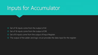
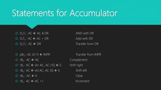
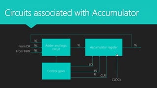
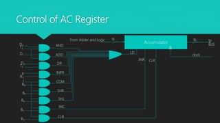
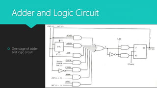
ACCUMULATOR LOGIC
BY : SHIVAM BHARTI 
Inputs for Accumulator
 Set of 16 inputs come from the output of AC.
 Set of 16 inputs come from the output of DR.
 Set of 8 inputs come from the output of Input Register.
 The output of the adder and logic circuit provides the data input for the register.
Statements for Accumulator
 D0T5 : AC  AC ٨ DR AND with DR
 D1T5 : AC  AC + DR Add with DR
 D2T5 : AC  DR Transfer from DR
 pB11 : AC (0-7)  INPR Transfer from INPR
 rB9 : AC  AC Complement
 rB7 : AC  shr AC, AC (15)  E Shift right
 rB6 : AC  shl AC, AC (0)  E Shift left
 rB11 : AC  0 Clear
 rB5 : AC  AC +1 Increment
Circuits associated with Accumulator
Adder and logic
circuit
Accumulator register
Control gates
16
16
16
From DR
From INPR
16 16
LD
IN
R CLR
CLOCK
Control of AC Register
AccumulatorD0
T5
B9
D1
D2
r
B11
B7
B11
B5
B6
p
T5
AND
ADD
DR
INPR
COM
SHR
SHL
INC
CLR
16 16 to
BUS
clock
LD
INR CLR
From Adder and Logic
Control of AC Register……….
 The control function for the clear micro-operation is rB11 , where r = D7I’T3 and B11=IR(11).
 The output of the AND gate that generates this control function is connected to the CLR input of
the INR input of the register.
 The seven micro-operation are generated in the adder and logic circuit and are loaded into AC
at proper time.
Adder and Logic Circuit
 One stage of adder
and logic circuit
Stages of Adder and Logic circuit
 The adder and logic circuit can be sub-divided into 16 stages, with each bit corresponding to one
bit of AC.
 One stage of the adder and logic circuit consists of seven AND gates one OR gate and a full
adder (FA) as shown above.
 The input is labelled Ii output AC(i).
 When LD input is enabled, the 16 inputs Ii for i=0,1,2…15 are transferred to AC(i).
 The AND operation is achieved by AND ing AC(i) with the corresponding bit in DR(i).
 The transfer from INPR to AC is only for bits 0 through 7.
 The complement micro-operation is obtained by inverting the bit value in AC.
 Shift-right operation transfers bit from AC(i+1) and shift-left operation transfers the bit from AC(i-
1).
 The complete adder and logic circuit consists of 16 stages connected together.
Thanks………… 

Acc logic

  • 1.
    ACCUMULATOR LOGIC BY :SHIVAM BHARTI 
  • 2.
    Inputs for Accumulator Set of 16 inputs come from the output of AC.  Set of 16 inputs come from the output of DR.  Set of 8 inputs come from the output of Input Register.  The output of the adder and logic circuit provides the data input for the register.
  • 3.
    Statements for Accumulator D0T5 : AC  AC ٨ DR AND with DR  D1T5 : AC  AC + DR Add with DR  D2T5 : AC  DR Transfer from DR  pB11 : AC (0-7)  INPR Transfer from INPR  rB9 : AC  AC Complement  rB7 : AC  shr AC, AC (15)  E Shift right  rB6 : AC  shl AC, AC (0)  E Shift left  rB11 : AC  0 Clear  rB5 : AC  AC +1 Increment
  • 4.
    Circuits associated withAccumulator Adder and logic circuit Accumulator register Control gates 16 16 16 From DR From INPR 16 16 LD IN R CLR CLOCK
  • 5.
    Control of ACRegister AccumulatorD0 T5 B9 D1 D2 r B11 B7 B11 B5 B6 p T5 AND ADD DR INPR COM SHR SHL INC CLR 16 16 to BUS clock LD INR CLR From Adder and Logic
  • 6.
    Control of ACRegister……….  The control function for the clear micro-operation is rB11 , where r = D7I’T3 and B11=IR(11).  The output of the AND gate that generates this control function is connected to the CLR input of the INR input of the register.  The seven micro-operation are generated in the adder and logic circuit and are loaded into AC at proper time.
  • 7.
    Adder and LogicCircuit  One stage of adder and logic circuit
  • 8.
    Stages of Adderand Logic circuit  The adder and logic circuit can be sub-divided into 16 stages, with each bit corresponding to one bit of AC.  One stage of the adder and logic circuit consists of seven AND gates one OR gate and a full adder (FA) as shown above.  The input is labelled Ii output AC(i).  When LD input is enabled, the 16 inputs Ii for i=0,1,2…15 are transferred to AC(i).  The AND operation is achieved by AND ing AC(i) with the corresponding bit in DR(i).  The transfer from INPR to AC is only for bits 0 through 7.  The complement micro-operation is obtained by inverting the bit value in AC.  Shift-right operation transfers bit from AC(i+1) and shift-left operation transfers the bit from AC(i- 1).  The complete adder and logic circuit consists of 16 stages connected together.
  • 9.