Downloaded 418 times
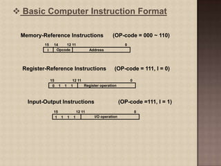

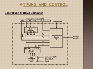
![INSTRUCTION CYCLEIn basic computer each instruction cycle consist of following phases:-1. Fetch an instruction from the memory.2. Decode the instruction. 3. Read the effective address from the memory if the instruction has an indirect address. 4. Execute the instruction.Fetch & decode ->Initially, the PC is loaded with the address of the first incrementer in the program. The SC(sequence counter) is cleared to 0,providing a decoded time signal T0.After each clock pulse ,SC is incremented by1 so that the timing go through a sequenceT0,T1,T3 and so on . The microperations for fetch & decode phases are:- T0: AR<-PC T1: IR<-M[AR],PC<-PC+1 T2: D0…..,D7<-Decode IR(12-14),AR<-IR(0-11),I<-IR(15)](https://image.slidesharecdn.com/computerinstruction-110818112455-phpapp01/85/Computer-instruction-10-320.jpg)
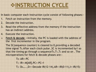
![FETCH and DECODE• Fetch and DecodeT0: AR PC (S0S1S2=010, T0=1)T1: IR M [AR], PC PC + 1 (S0S1S2=111, T1=1)T2: D0, . . . , D7 Decode IR(12-14), AR IR(0-11), I IR(15)T1S2BusT0S1S0Memory7unitAddressReadAR1LDPC2INRIR5LDClockCommon bus](https://image.slidesharecdn.com/computerinstruction-110818112455-phpapp01/85/Computer-instruction-11-320.jpg)

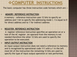
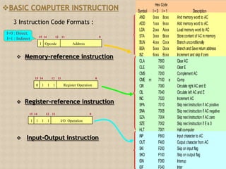
1. The document discusses the topics of computer instructions, timing and control, and the instruction cycle for a basic computer. 2. It describes the three instruction code formats used - memory reference, register reference, and input/output. Memory reference instructions use bits to specify an address and addressing mode. Register reference instructions specify an operation on the accumulator register. 3. The instruction cycle consists of four phases - fetch an instruction, decode the instruction, read the effective address if needed, and execute the instruction.