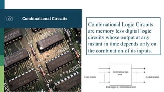
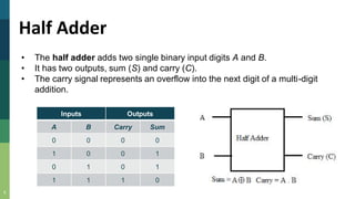
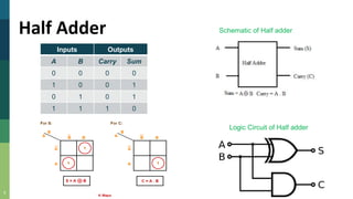
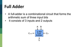
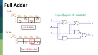
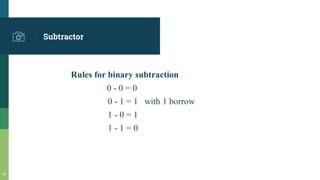
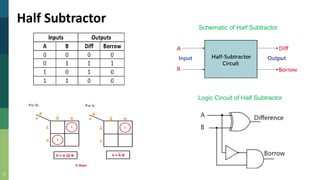
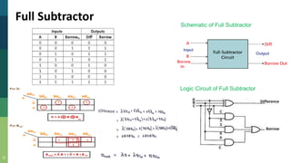
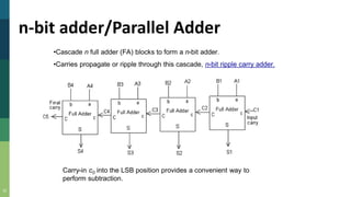
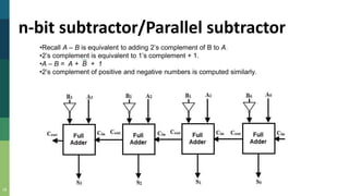
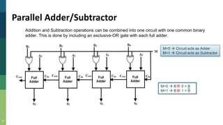
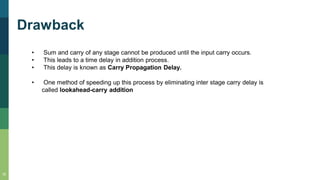
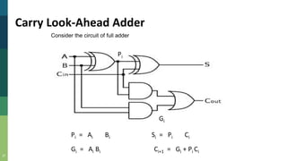
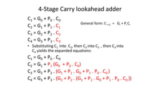
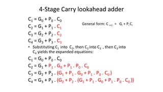
UNIT II
COMBINATIONAL AND SEQUENTIAL CIRCUITS
1
AD8252 - Digital Principles and Computer Organization
Syllabus
Combinational circuits – Adder – Subtractor –
ALU Design – Decoder – Encoder –
Multiplexers – Introduction to Sequential
Circuits – Flip-Flops – Registers – Counters.
2
Combinational Circuits
Combinational Logic Circuits
are memory less digital logic
circuits whose output at any
instant in time depends only on
the combination of its inputs.
3
Adder
4
Rules for binary addition
0 + 0 = 0
0 + 1 = 1
1 + 0 = 1
1 + 1 = 102
5
Half Adder
• The half adder adds two single binary input digits A and B.
• It has two outputs, sum (S) and carry (C).
• The carry signal represents an overflow into the next digit of a multi-digit
addition.
Inputs Outputs
A B Carry Sum
0 0 0 0
1 0 0 1
0 1 0 1
1 1 1 0
6
Half Adder
Inputs Outputs
A B Carry Sum
0 0 0 0
1 0 0 1
0 1 0 1
1 1 1 0
Schematic of Half adder
Logic Circuit of Half adder
7
Full Adder
• A full-adder is a combinational circuit that forms the
arithmetic sum of three input bits
• It consists of 3 inputs and 2 outputs
8
Full Adder
9
Full Adder
Logic Diagram of Full Adder
Subtractor
10
Rules for binary subtraction
0 - 0 = 0
0 - 1 = 1 with 1 borrow
1 - 0 = 1
1 - 1 = 0
11
Half Subtractor
Schematic of Half Subtractor
Logic Circuit of Half Subtractor
12
Full Subtractor
Schematic of Full Subtractor
Logic Circuit of Full Subtractor
13
n-bit adder/Parallel Adder
•Cascade n full adder (FA) blocks to form a n-bit adder.
•Carries propagate or ripple through this cascade, n-bit ripple carry adder.
Carry-in c0 into the LSB position provides a convenient way to
perform subtraction.
14
n-bit subtractor/Parallel subtractor
•Recall A – B is equivalent to adding 2’s complement of B to A.
•2’s complement is equivalent to 1’s complement + 1.
•A – B = A + B + 1
•2’s complement of positive and negative numbers is computed similarly.
15
Parallel Adder/Subtractor
Addition and Subtraction operations can be combined into one circuit with one common binary
adder. This is done by including an exclusive-OR gate with each full adder.
M=0  Circuit acts as Adder
M=1  Circuit acts as Subtractor
M=0  B 0 = B
M=1  B 1 = B
16
Drawback
• Sum and carry of any stage cannot be produced until the input carry occurs.
• This leads to a time delay in addition process.
• This delay is known as Carry Propagation Delay.
• One method of speeding up this process by eliminating inter stage carry delay is
called lookahead-carry addition
17
Carry Look-Ahead Adder
Consider the circuit of full adder
Pi
Gi
Pi = Ai Bi Si = Pi Ci
Gi = Ai Bi Ci+1 = Gi + Pi Ci
4-Stage Carry lookahead adder
C1 = G0 + P0 . C0
C2 = G1 + P1 . C1
C3 = G2 + P2 . C2
C4 = G3 + P3 . C3
• Substituting C1 into C2, then C2 into C3 , then C3 into
C4 yields the expanded equations:
C1 = G0 + P0 . C0
C2 = G1 + P1 (G0 + P0 . C0)
C3 = G2 + P2 . (G1 + P1 . G0 + P1 . P0 . C0 )
C4 = G3 + P3 . (G2 + P2 . (G1 + P1 . G0 + P1 . P0 . C0 ))
General form: C i+1 = Gi + Pi Ci
4-Stage Carry lookahead adder
C1 = G0 + P0 . C0
C2 = G1 + P1 . C1
C3 = G2 + P2 . C2
C4 = G3 + P3 . C3
• Substituting C1 into C2, then C2 into C3 , then C3 into
C4 yields the expanded equations:
C1 = G0 + P0 . C0
C2 = G1 + P1 . G0 + P1 . P0 . C0
C3 = G2 + P2 . (G1 + P1 . G0 + P1 . P0 . C0 )
C4 = G3 + P3 . (G2 + P2 . (G1 + P1 . G0 + P1 . P0 . C0 ))
General form: C i+1 = Gi + Pi Ci
4- bit Carry-lookahead adder
ALU Design
21
Symbol of ALU
ALU is responsible to perform
the operations in the computer
ALU Design
22
Symbol of ALU

DPCO-Unit 2-Combinational Circuit.pdf

  • 1.
    UNIT II COMBINATIONAL ANDSEQUENTIAL CIRCUITS 1 AD8252 - Digital Principles and Computer Organization
  • 2.
    Syllabus Combinational circuits –Adder – Subtractor – ALU Design – Decoder – Encoder – Multiplexers – Introduction to Sequential Circuits – Flip-Flops – Registers – Counters. 2
  • 3.
    Combinational Circuits Combinational LogicCircuits are memory less digital logic circuits whose output at any instant in time depends only on the combination of its inputs. 3
  • 4.
    Adder 4 Rules for binaryaddition 0 + 0 = 0 0 + 1 = 1 1 + 0 = 1 1 + 1 = 102
  • 5.
    5 Half Adder • Thehalf adder adds two single binary input digits A and B. • It has two outputs, sum (S) and carry (C). • The carry signal represents an overflow into the next digit of a multi-digit addition. Inputs Outputs A B Carry Sum 0 0 0 0 1 0 0 1 0 1 0 1 1 1 1 0
  • 6.
    6 Half Adder Inputs Outputs AB Carry Sum 0 0 0 0 1 0 0 1 0 1 0 1 1 1 1 0 Schematic of Half adder Logic Circuit of Half adder
  • 7.
    7 Full Adder • Afull-adder is a combinational circuit that forms the arithmetic sum of three input bits • It consists of 3 inputs and 2 outputs
  • 8.
  • 9.
  • 10.
    Subtractor 10 Rules for binarysubtraction 0 - 0 = 0 0 - 1 = 1 with 1 borrow 1 - 0 = 1 1 - 1 = 0
  • 11.
    11 Half Subtractor Schematic ofHalf Subtractor Logic Circuit of Half Subtractor
  • 12.
    12 Full Subtractor Schematic ofFull Subtractor Logic Circuit of Full Subtractor
  • 13.
    13 n-bit adder/Parallel Adder •Cascaden full adder (FA) blocks to form a n-bit adder. •Carries propagate or ripple through this cascade, n-bit ripple carry adder. Carry-in c0 into the LSB position provides a convenient way to perform subtraction.
  • 14.
    14 n-bit subtractor/Parallel subtractor •RecallA – B is equivalent to adding 2’s complement of B to A. •2’s complement is equivalent to 1’s complement + 1. •A – B = A + B + 1 •2’s complement of positive and negative numbers is computed similarly.
  • 15.
    15 Parallel Adder/Subtractor Addition andSubtraction operations can be combined into one circuit with one common binary adder. This is done by including an exclusive-OR gate with each full adder. M=0  Circuit acts as Adder M=1  Circuit acts as Subtractor M=0  B 0 = B M=1  B 1 = B
  • 16.
    16 Drawback • Sum andcarry of any stage cannot be produced until the input carry occurs. • This leads to a time delay in addition process. • This delay is known as Carry Propagation Delay. • One method of speeding up this process by eliminating inter stage carry delay is called lookahead-carry addition
  • 17.
    17 Carry Look-Ahead Adder Considerthe circuit of full adder Pi Gi Pi = Ai Bi Si = Pi Ci Gi = Ai Bi Ci+1 = Gi + Pi Ci
  • 18.
    4-Stage Carry lookaheadadder C1 = G0 + P0 . C0 C2 = G1 + P1 . C1 C3 = G2 + P2 . C2 C4 = G3 + P3 . C3 • Substituting C1 into C2, then C2 into C3 , then C3 into C4 yields the expanded equations: C1 = G0 + P0 . C0 C2 = G1 + P1 (G0 + P0 . C0) C3 = G2 + P2 . (G1 + P1 . G0 + P1 . P0 . C0 ) C4 = G3 + P3 . (G2 + P2 . (G1 + P1 . G0 + P1 . P0 . C0 )) General form: C i+1 = Gi + Pi Ci
  • 19.
    4-Stage Carry lookaheadadder C1 = G0 + P0 . C0 C2 = G1 + P1 . C1 C3 = G2 + P2 . C2 C4 = G3 + P3 . C3 • Substituting C1 into C2, then C2 into C3 , then C3 into C4 yields the expanded equations: C1 = G0 + P0 . C0 C2 = G1 + P1 . G0 + P1 . P0 . C0 C3 = G2 + P2 . (G1 + P1 . G0 + P1 . P0 . C0 ) C4 = G3 + P3 . (G2 + P2 . (G1 + P1 . G0 + P1 . P0 . C0 )) General form: C i+1 = Gi + Pi Ci
  • 20.
  • 21.
    ALU Design 21 Symbol ofALU ALU is responsible to perform the operations in the computer
  • 22.