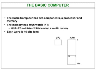
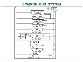
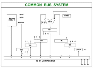
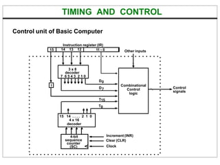
The document provides an overview of computer organization and architecture. It discusses the basic components of a computer including the CPU, memory, and registers. It then describes the specific architecture of a basic computer model, including its instruction set, addressing modes, and register set. The basic computer uses a 16-bit word size and has instructions for memory access, register operations, and input/output. It connects its registers through a common 16-bit bus controlled by three lines.

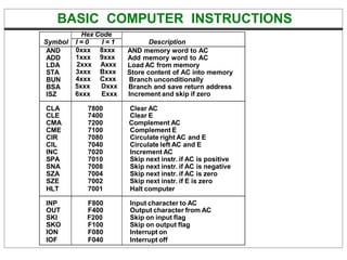
![DETERMINE THE TYPE OF INSTRUCTION
= 0 (direct)
D'7IT3:
D'7I'T3:
D7I'T3:
D7IT3:
AR M[AR]
Nothing
Execute a register-reference instr.
Execute an input-output instr.
Start
SC
AR PC
T0
IR M[AR], PC PC + 1
T1
Decode Opcode in IR(12-14),
AR IR(0-11), I IR(15)
T2
D7
(Register or I/O) = 1 = 0 (Memory-reference)
I
I
Execute
register-reference
instruction
SC 0
Execute
input-output
instruction
SC 0
AR M[AR] Nothing
(I/O) = 1 = 0 (register) (indirect) = 1
T3 T3 T3 T3
Execute
memory-reference
instruction
SC 0
T4
Memory
Fetch
Decode
Execute
Fetch
Decode
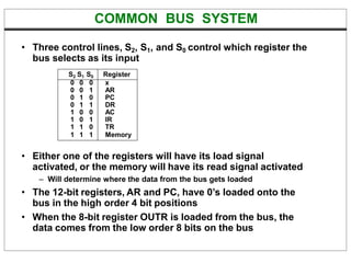
S2 S1 S0 Register
0 0 0 x
0 0 1 AR
0 1 0 PC
0 1 1 DR
1 0 0 AC
1 0 1 IR
1 1 0 TR
1 1 1 Memory
14, 13 ,12
Instruction register (IR)
15 14 13 12 11 - 0](https://image.slidesharecdn.com/ch5morrismano-230212170134-caa658a6/85/Ch5_MorrisMano-pptx-30-320.jpg)
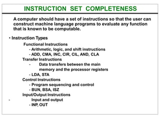
![FETCH and DECODE
• Fetch and Decode T0: AR PC (S0S1S2=010, T0=1)
T1: IR M [AR], PC PC + 1 (S0S1S2=111, T1=1)
T2: D0, . . . , D7 Decode IR(12-14),AR IR(0-11), I IR(15)
S2
S1
S0
Bus
7
Memory
unit
Address
Read
AR
LD
PC
INR
IR
LD Clock
1
2
5
Common bus
T1
T0
S2 S1 S0 Register
0 0 0 x
0 0 1 AR
0 1 0 PC
0 1 1 DR
1 0 0 AC
1 0 1 IR
1 1 0 TR
1 1 1 Memory
Instruction register (IR)
15 14 13 12 11 - 0](https://image.slidesharecdn.com/ch5morrismano-230212170134-caa658a6/85/Ch5_MorrisMano-pptx-32-320.jpg)
![MEMORY REFERENCE INSTRUCTIONS
DR M[AR]
AC AC DR, SC 0
Read operand
AND with AC
D0T4:
D0T5:
ADD to AC
D1T4:
D1T5:
DR M[AR]
AC AC + DR, E Cout, SC 0
Read operand
Add to AC and store carry in E
- The effective address of the instruction is in AR and was placed there during
timing signal T2 when I = 0, or during timing signal T3 when I = 1
- Memory cycle is assumed to be short enough to complete in a CPU cycle
- The execution of MR instruction starts with T4
AND to AC
Symbol
Operation
Decoder
Symbolic Description
AND
ADD
LDA
STA
BUN
BSA
ISZ
D0
D1
D2
D3
D4
D5
D6
AC AC M[AR]
AC AC + M[AR], E Cout
AC M[AR]
M[AR] AC
PC AR
M[AR] PC, PC AR + 1
M[AR] M[AR] + 1, if M[AR] + 1 = 0 then PC PC+1](https://image.slidesharecdn.com/ch5morrismano-230212170134-caa658a6/85/Ch5_MorrisMano-pptx-34-320.jpg)
![MEMORY REFERENCE INSTRUCTIONS
Memory, PC after execution
20
PC = 21
AR = 135
136
0 BSA 135
Next instruction
Subroutine
1 BUN 135
20
21
135
PC = 136
0 BSA 135
Next instruction
21
Subroutine
1 BUN 135
Memory Memory
LDA: Load to AC
D2T4: DR M[AR]
D2T5: AC DR, SC 0
STA: Store AC
D3T4: M[AR] AC, SC 0
BUN: Branch Unconditionally
D4T4: PC AR, SC 0
BSA: Branch and Save Return Address
M[AR] PC, PC AR + 1
Memory, PC, AR at time T4](https://image.slidesharecdn.com/ch5morrismano-230212170134-caa658a6/85/Ch5_MorrisMano-pptx-35-320.jpg)
![MEMORY REFERENCE INSTRUCTIONS
BSA:
D5T4: M[AR] PC, AR AR + 1
D5T5: PC AR, SC 0
ISZ: Increment and Skip-if-Zero
D6T4: DR M[AR]
D6T5: DR DR + 1
D6T4: M[AR] DR, if (DR = 0) then (PC PC + 1), SC 0](https://image.slidesharecdn.com/ch5morrismano-230212170134-caa658a6/85/Ch5_MorrisMano-pptx-36-320.jpg)
![FLOWCHART FOR MEMORY REFERENCE INSTRUCTIONS
DR M[AR] DR M[AR] DR M[AR] M[AR] AC
SC 0
AND STA
AC AC + DR
E Cout
SC 0
AC DR
SC 0
D0T4
Memory-reference instruction
ADD LDA
D1T4 D2T4 D3T4
D0T5 D1T5 D2T5
PC AR
SC 0
M[AR] PC
AR AR + 1
DR M[AR]
BUN BSA ISZ
D4T4 D5T4 D6T4
DR DR + 1
D5T5 D6T5
PC AR
SC 0
M[AR] DR
If (DR = 0)
then (PC PC + 1)
SC 0
D6T6
AC AC DR
SC 0](https://image.slidesharecdn.com/ch5morrismano-230212170134-caa658a6/85/Ch5_MorrisMano-pptx-37-320.jpg)