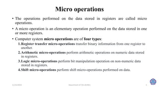
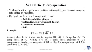
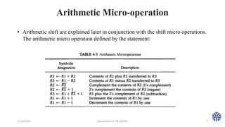
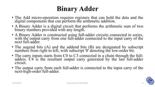
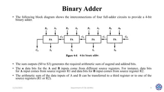
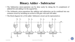
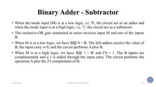
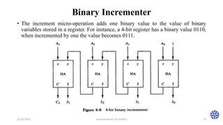
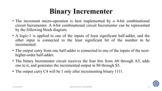
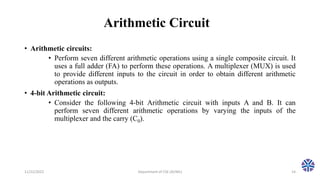
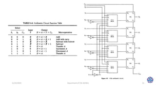
Tamil Call Girls Bhayandar WhatsApp +91-9930687706, Best Service
CS304PC:Computer Organization and Architecture Session 3 micro operations.pptx
1. CS307PC:Computer Organization
and Architecture (R18 II(I sem))
Department of computer science and engineering
(AI/ML)
Session 3
by
Asst.Prof.M.Gokilavani
VITS
11/22/2022 Department of CSE (AI/ML) 1
2. TEXT BOOK:
• 1. Computer System Architecture – M. Moris Mano, Third Edition,
Pearson/PHI.
REFERENCES:
• Computer Organization – Car Hamacher, Zvonks Vranesic, Safea
Zaky, Vth Edition, McGraw Hill.
• Computer Organization and Architecture – William Stallings Sixth
Edition, Pearson/PHI.
• Structured Computer Organization – Andrew S. Tanenbaum, 4th
Edition, PHI/Pearson.
11/22/2022 Department of CSE (AI/ML) 2
3. UNIT - I
11/22/2022 Department of CSE (AI/ML) 3
Digital Computers: Introduction, Block diagram of Digital Computer,
Definition of Computer Organization, Computer Design and Computer
Architecture.
Register Transfer Language and Micro operations: Register Transfer
language, Register Transfer, Bus and memory transfers, Arithmetic
Micro operations, logic micro operations, shift micro operations,
Arithmetic logic shift unit.
Basic Computer Organization and Design: Instruction codes,
Computer Registers Computer instructions, Timing and Control,
Instruction cycle, Memory Reference Instructions, Input – Output and
Interrupt.
4. Topics covered in session 3
• Register Transfer Language and Micro operations
• Register Transfer language
• Register Transfer
• Bus and memory transfers
• Arithmetic Micro operations
• logic micro operations
• shift micro operations
• Arithmetic logic shift unit
11/22/2022 Department of CSE (AI/ML) 4
5. Micro operations
• The operations performed on the data stored in registers are called micro
operations.
• A micro operation is an elementary operation performed on the data stored in one
or more registers.
• Computer system micro operations are of four types:
1.Register transfer micro-operations transfer binary information from one register to
another.
2.Arithmetic micro-operations perform arithmetic operations on numeric data stored
in registers.
3.Logic micro-operations perform bit manipulation operation on non-numeric data
stored in registers.
4.Shift micro-operations perform shift micro-operations performed on data.
11/22/2022 Department of CSE (AI/ML) 5
6. Arithmetic Micro-operation
• Arithmetic micro operations perform arithmetic operations on numeric
data stored in registers.
• The basic arithmetic micro operations are
• Addition, Addition with carry
• Subtraction, subtraction with borrow
• Increment/Decrement
• Shift.
Example:
Assume that th input data are in register R1, 𝑅2 is th symbol for 1’s
complement of R2. Adding 1 to th 1’s complement produces the 2’s
complement. Adding th contents of R1 to the 2’s complement of R2 is
equivalent to R1-R2.
11/22/2022 Department of CSE (AI/ML) 6
7. Arithmetic Micro-operation
11/22/2022 Department of CSE (AI/ML) 7
• Arithmetic shift are explained later in conjunction with the shift micro operations.
The arithmetic micro operation defined by the statement:
8. Binary Adder
• The Add micro-operation requires registers that can hold the data and the
digital components that can perform the arithmetic addition.
• A Binary Adder is a digital circuit that performs the arithmetic sum of two
binary numbers provided with any length.
• A Binary Adder is constructed using full-adder circuits connected in series,
with the output carry from one full-adder connected to the input carry of the
next full-adder.
• The augend bits (A) and the addend bits (B) are designated by subscript
numbers from right to left, with subscript '0' denoting the low-order bit.
• The carry inputs starts from C0 to C3 connected in a chain through the full-
adders. C4 is the resultant output carry generated by the last full-adder
circuit.
• The output carry from each full-adder is connected to the input carry of the
next-high-order full-adder.
11/22/2022 Department of CSE (AI/ML) 8
9. Binary Adder
• The following block diagram shows the interconnections of four full-adder circuits to provide a 4-bit
binary adder.
• The sum outputs (S0 to S3) generates the required arithmetic sum of augend and addend bits.
• The n data bits for the A and B inputs come from different source registers. For instance, data bits
for A input comes from source register R1 and data bits for B input comes from source register R2.
• The arithmetic sum of the data inputs of A and B can be transferred to a third register or to one of the
source registers (R1 or R2).
11/22/2022 Department of CSE (AI/ML) 9
10. Binary Adder - Subtractor
• The Subtraction micro-operation can be done easily by taking the 2's compliment of
addend bits and adding it to the augend bits.
• The Arithmetic micro-operations like addition and subtraction can be combined into one
common circuit by including an exclusive-OR gate with each full adder.
• The block diagram for a 4-bit adder- Subtractor circuit can be represented as:
11/22/2022 Department of CSE (AI/ML) 10
11. Binary Adder - Subtractor
• When the mode input (M) is at a low logic, i.e. '0', the circuit act as an adder and
when the mode input is at a high logic, i.e. '1', the circuit act as a subtractor.
• The exclusive-OR gate connected in series receives input M and one of the inputs
B.
• When M is at a low logic, we have B⊕ 0 = B. The full-adders receive the value of
B, the input carry is 0, and the circuit performs A plus B.
• When M is at a high logic, we have B⊕ 1 = B' and C0 = 1. The B inputs are
complemented, and a 1 is added through the input carry. The circuit performs the
operation A plus the 2's complement of B.
11/22/2022 Department of CSE (AI/ML) 11
12. Binary Incrementer
• The increment micro-operation adds one binary value to the value of binary
variables stored in a register. For instance, a 4-bit register has a binary value 0110,
when incremented by one the value becomes 0111.
11/22/2022 Department of CSE (AI/ML) 12
13. Binary Incrementer
• The increment micro-operation is best implemented by a 4-bit combinational
circuit Incrementer. A 4-bit combinational circuit Incrementer can be represented
by the following block diagram.
• A logic-1 is applied to one of the inputs of least significant half-adder, and the
other input is connected to the least significant bit of the number to be
incremented.
• The output carry from one half-adder is connected to one of the inputs of the next-
higher-order half-adder.
• The binary Incrementer circuit receives the four bits from A0 through A3, adds
one to it, and generates the incremented output in S0 through S3.
• The output carry C4 will be 1 only after incrementing binary 1111.
11/22/2022 Department of CSE (AI/ML) 13
14. Arithmetic Circuit
• Arithmetic circuits:
• Perform seven different arithmetic operations using a single composite circuit. It
uses a full adder (FA) to perform these operations. A multiplexer (MUX) is used
to provide different inputs to the circuit in order to obtain different arithmetic
operations as outputs.
• 4-bit Arithmetic circuit:
• Consider the following 4-bit Arithmetic circuit with inputs A and B. It can
perform seven different arithmetic operations by varying the inputs of the
multiplexer and the carry (C0).
11/22/2022 Department of CSE (AI/ML) 14
16. Topics to be covered in next session 4
• Logic micro operations, Shift micro operations, Arithmetic shift
logic unit
11/22/2022 Department of CSE (AI/ML) 16
Thank you!!!