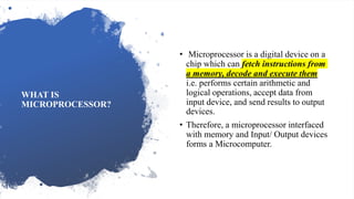
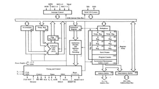
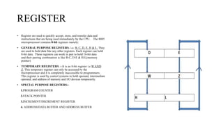
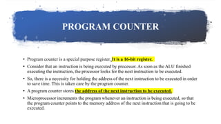
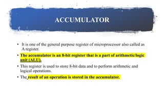
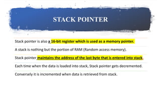
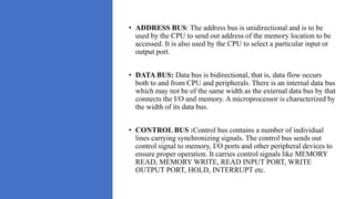
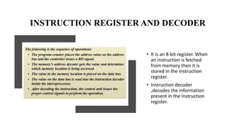
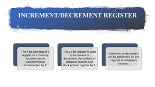
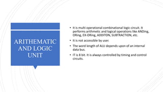
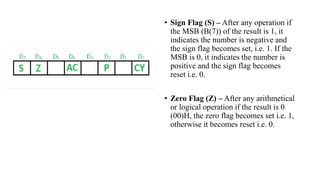
8085
MICROPROCESSOR
ARCHITECTURE
WHAT IS
MICROPROCESSOR?
• Microprocessor is a digital device on a
chip which can fetch instructions from
a memory, decode and execute them
i.e. performs certain arithmetic and
logical operations, accept data from
input device, and send results to output
devices.
• Therefore, a microprocessor interfaced
with memory and Input/ Output devices
forms a Microcomputer.
REGISTER
• Register are used to quickly accept, store, and transfer data and
instructions that are being used immediately by the CPU. The 8085
microprocessor contains 8-bit registers namely:
• GENERAL PURPOSE REGISTERS- i.e. B, C, D, E, H & L. They
are used to hold data like any other registers. Each register can hold
8-bit data. These registers can work in pair to hold 16-bit data
and their pairing combination is like B-C, D-E & H-L(memory
pointer)
• TEMPORARY REGISTERS :--It is an 8-bit register i.e W AND
Z. This temporary register can only be accessed by the
microprocessor and it is completely inaccessible to programmers.
This register is used by control systems to hold operand, intermediate
operand, and address of memory and I/O devices temporarily.
• SPECIAL PURPOSE REGISTERS:-
1.PROGRAM COUNTER
2.STACK POINTER
3.INCREMENT/DECREMENT REGISTER
4. ADDRESS/DATA BUFFER AND ADDRESS BUFFER
PROGRAM COUNTER
• Program counter is a special purpose register. It is a 16-bit register.
• Consider that an instruction is being executed by processor. As soon as the ALU finished
executing the instruction, the processor looks for the next instruction to be executed.
• So, there is a necessity for holding the address of the next instruction to be executed in order
to save time. This is taken care by the program counter.
• A program counter stores the address of the next instruction to be executed.
• Microprocessor increments the program whenever an instruction is being executed, so that
the program counter points to the memory address of the next instruction that is going to be
executed.
ACCUMULATOR
• It is one of the general purpose register of microprocessor also called as
A register.
• The accumulator is an 8-bit register that is a part of arithmetic/logic
unit (ALU).
• This register is used to store 8-bit data and to perform arithmetic and
logical operations.
• The result of an operation is stored in the accumulator.
STACK POINTER
Stack pointer is also a 16-bit register which is used as a memory pointer.
A stack is nothing but the portion of RAM (Random access memory).
Stack pointer maintains the address of the last byte that is entered into stack.
Each time when the data is loaded into stack, Stack pointer gets decremented.
Conversely it is incremented when data is retrieved from stack.
• ADDRESS BUS: The address bus is unidirectional and is to be
used by the CPU to send out address of the memory location to be
accessed. It is also used by the CPU to select a particular input or
output port.
• DATA BUS: Data bus is bidirectional, that is, data flow occurs
both to and from CPU and peripherals. There is an internal data bus
which may not be of the same width as the external data bus by that
connects the I/O and memory. A microprocessor is characterized by
the width of its data bus.
• CONTROL BUS :Control bus contains a number of individual
lines carrying synchronizing signals. The control bus sends out
control signal to memory, I/O ports and other peripheral devices to
ensure proper operation. It carries control signals like MEMORY
READ, MEMORY WRITE, READ INPUT PORT, WRITE
OUTPUT PORT, HOLD, INTERRUPT etc.
INSTRUCTION REGISTER AND DECODER
• It is an 8-bit register. When
an instruction is fetched
from memory then it is
stored in the Instruction
register.
• Instruction decoder
,decodes the information
present in the Instruction
register.
INCREMENT/DECREMENT REGISTER
The 8-bit contents of a
register or a memory
location can be
incremented or
decremented by 1.
This 16-bit register is used
to increment or
decrement the content of
program counter and
stack pointer register by 1.
Increment or decrement
can be performed on any
register or a memory
location.
ARITHEMATIC
AND LOGIC
UNIT
• It is multi operational combinational logic circuit. It
performs arithmetic and logical operations like ANDing,
ORing, EX-ORing, ADDITON, SUBTRACTION, etc.
• It is not accessible by user.
• The word length of ALU depends upon of an internal
data bus.
• IT is 8 bit. It is always controlled by timing and control
circuits.
FLAG REGISTER
• It is an 8-bit register having five 1-bit flip-flops, which holds either 0 or 1 depending upon the result stored in the
accumulator.
• It tells CURRENT status of result.
• These are the set of 5 flags −
1. Sign (S)
2. Zero (Z)
3. Auxiliary Carry (AC)
4. Parity (P)
5. Carry (C)
• Sign Flag (S) – After any operation if
the MSB (B(7)) of the result is 1, it
indicates the number is negative and
the sign flag becomes set, i.e. 1. If the
MSB is 0, it indicates the number is
positive and the sign flag becomes
reset i.e. 0.
• Zero Flag (Z) – After any arithmetical
or logical operation if the result is 0
(00)H, the zero flag becomes set i.e. 1,
otherwise it becomes reset i.e. 0.
• Auxiliary Cary Flag (AC) – This flag is
used in BCD number system(0-9). If after
any arithmetic or logical operation D(3)
generates any carry and passes on to B(4) this
flag becomes set i.e. 1, otherwise it becomes
reset i.e. 0.
• Parity Flag (P) – If after any arithmetic
or logical operation the result has even parity,
an even number of 1 bits, the parity
register becomes set i.e. 1, otherwise it
becomes reset i.e. 0.
• 1-accumulator has even number of 1 bits
0-accumulator has odd parity
Carry Flag (CY) – Carry is
generated when performing n bit
operations and the result is more
than n bits, then this flag becomes
set i.e. 1, otherwise it becomes
reset i.e. 0.
ADDRESS/DATA BUFFER
AND ADDRESS BUFFER
• The contents of the stack pointer and program counter
are loaded into the address buffer and address-data
buffer.
• As the memory and I/O chips are connected to these
buses, the CPU can exchange desired data to the memory
and I/O chips.
• The address-data buffer is not only connected to the
external data bus but also to the internal data bus which
consists of 8-bits.
TIMING
AND CONTROL
• It provides timing and control signal to
the microprocessor to perform
operations. Following are the timing
and control signals, which control
external and internal circuits −
• Control Signals: READY, RD’, WR’,
ALE
• Status Signals: S0, S1, IO/M’
• DMA Signals: HOLD, HLDA
• RESET Signals: RESET IN, RESET
OUT
SERIAL I/O CONTROL SECTION
The input and output of
serial data can be carried
out using 2 instructions in
8085:
1. SID-Serial Input Data
2. SOD-Serial Output Data
Two more instructions are
used to perform serial-
parallel conversion needed
for serial I/O devices
INTERRUPT CONTROL
As the name suggests it controls the interrupts during a process.
When a microprocessor is executing a main program and whenever an interrupt occurs,
the microprocessor shifts the control from the main program to process the incoming
request. After the request is completed, the control goes back to the main program.
There are 5 interrupt signals in 8085 microprocessor: INTR, RST 7.5, RST 6.5, RST 5.5,
TRAP.

8085 microprocessor architecture

  • 1.
  • 2.
    WHAT IS MICROPROCESSOR? • Microprocessoris a digital device on a chip which can fetch instructions from a memory, decode and execute them i.e. performs certain arithmetic and logical operations, accept data from input device, and send results to output devices. • Therefore, a microprocessor interfaced with memory and Input/ Output devices forms a Microcomputer.
  • 4.
    REGISTER • Register areused to quickly accept, store, and transfer data and instructions that are being used immediately by the CPU. The 8085 microprocessor contains 8-bit registers namely: • GENERAL PURPOSE REGISTERS- i.e. B, C, D, E, H & L. They are used to hold data like any other registers. Each register can hold 8-bit data. These registers can work in pair to hold 16-bit data and their pairing combination is like B-C, D-E & H-L(memory pointer) • TEMPORARY REGISTERS :--It is an 8-bit register i.e W AND Z. This temporary register can only be accessed by the microprocessor and it is completely inaccessible to programmers. This register is used by control systems to hold operand, intermediate operand, and address of memory and I/O devices temporarily. • SPECIAL PURPOSE REGISTERS:- 1.PROGRAM COUNTER 2.STACK POINTER 3.INCREMENT/DECREMENT REGISTER 4. ADDRESS/DATA BUFFER AND ADDRESS BUFFER
  • 5.
    PROGRAM COUNTER • Programcounter is a special purpose register. It is a 16-bit register. • Consider that an instruction is being executed by processor. As soon as the ALU finished executing the instruction, the processor looks for the next instruction to be executed. • So, there is a necessity for holding the address of the next instruction to be executed in order to save time. This is taken care by the program counter. • A program counter stores the address of the next instruction to be executed. • Microprocessor increments the program whenever an instruction is being executed, so that the program counter points to the memory address of the next instruction that is going to be executed.
  • 6.
    ACCUMULATOR • It isone of the general purpose register of microprocessor also called as A register. • The accumulator is an 8-bit register that is a part of arithmetic/logic unit (ALU). • This register is used to store 8-bit data and to perform arithmetic and logical operations. • The result of an operation is stored in the accumulator.
  • 7.
    STACK POINTER Stack pointeris also a 16-bit register which is used as a memory pointer. A stack is nothing but the portion of RAM (Random access memory). Stack pointer maintains the address of the last byte that is entered into stack. Each time when the data is loaded into stack, Stack pointer gets decremented. Conversely it is incremented when data is retrieved from stack.
  • 8.
    • ADDRESS BUS:The address bus is unidirectional and is to be used by the CPU to send out address of the memory location to be accessed. It is also used by the CPU to select a particular input or output port. • DATA BUS: Data bus is bidirectional, that is, data flow occurs both to and from CPU and peripherals. There is an internal data bus which may not be of the same width as the external data bus by that connects the I/O and memory. A microprocessor is characterized by the width of its data bus. • CONTROL BUS :Control bus contains a number of individual lines carrying synchronizing signals. The control bus sends out control signal to memory, I/O ports and other peripheral devices to ensure proper operation. It carries control signals like MEMORY READ, MEMORY WRITE, READ INPUT PORT, WRITE OUTPUT PORT, HOLD, INTERRUPT etc.
  • 9.
    INSTRUCTION REGISTER ANDDECODER • It is an 8-bit register. When an instruction is fetched from memory then it is stored in the Instruction register. • Instruction decoder ,decodes the information present in the Instruction register.
  • 10.
    INCREMENT/DECREMENT REGISTER The 8-bitcontents of a register or a memory location can be incremented or decremented by 1. This 16-bit register is used to increment or decrement the content of program counter and stack pointer register by 1. Increment or decrement can be performed on any register or a memory location.
  • 11.
    ARITHEMATIC AND LOGIC UNIT • Itis multi operational combinational logic circuit. It performs arithmetic and logical operations like ANDing, ORing, EX-ORing, ADDITON, SUBTRACTION, etc. • It is not accessible by user. • The word length of ALU depends upon of an internal data bus. • IT is 8 bit. It is always controlled by timing and control circuits.
  • 12.
    FLAG REGISTER • Itis an 8-bit register having five 1-bit flip-flops, which holds either 0 or 1 depending upon the result stored in the accumulator. • It tells CURRENT status of result. • These are the set of 5 flags − 1. Sign (S) 2. Zero (Z) 3. Auxiliary Carry (AC) 4. Parity (P) 5. Carry (C)
  • 13.
    • Sign Flag(S) – After any operation if the MSB (B(7)) of the result is 1, it indicates the number is negative and the sign flag becomes set, i.e. 1. If the MSB is 0, it indicates the number is positive and the sign flag becomes reset i.e. 0. • Zero Flag (Z) – After any arithmetical or logical operation if the result is 0 (00)H, the zero flag becomes set i.e. 1, otherwise it becomes reset i.e. 0.
  • 14.
    • Auxiliary CaryFlag (AC) – This flag is used in BCD number system(0-9). If after any arithmetic or logical operation D(3) generates any carry and passes on to B(4) this flag becomes set i.e. 1, otherwise it becomes reset i.e. 0. • Parity Flag (P) – If after any arithmetic or logical operation the result has even parity, an even number of 1 bits, the parity register becomes set i.e. 1, otherwise it becomes reset i.e. 0. • 1-accumulator has even number of 1 bits 0-accumulator has odd parity Carry Flag (CY) – Carry is generated when performing n bit operations and the result is more than n bits, then this flag becomes set i.e. 1, otherwise it becomes reset i.e. 0.
  • 15.
    ADDRESS/DATA BUFFER AND ADDRESSBUFFER • The contents of the stack pointer and program counter are loaded into the address buffer and address-data buffer. • As the memory and I/O chips are connected to these buses, the CPU can exchange desired data to the memory and I/O chips. • The address-data buffer is not only connected to the external data bus but also to the internal data bus which consists of 8-bits.
  • 16.
    TIMING AND CONTROL • Itprovides timing and control signal to the microprocessor to perform operations. Following are the timing and control signals, which control external and internal circuits − • Control Signals: READY, RD’, WR’, ALE • Status Signals: S0, S1, IO/M’ • DMA Signals: HOLD, HLDA • RESET Signals: RESET IN, RESET OUT
  • 17.
    SERIAL I/O CONTROLSECTION The input and output of serial data can be carried out using 2 instructions in 8085: 1. SID-Serial Input Data 2. SOD-Serial Output Data Two more instructions are used to perform serial- parallel conversion needed for serial I/O devices
  • 18.
    INTERRUPT CONTROL As thename suggests it controls the interrupts during a process. When a microprocessor is executing a main program and whenever an interrupt occurs, the microprocessor shifts the control from the main program to process the incoming request. After the request is completed, the control goes back to the main program. There are 5 interrupt signals in 8085 microprocessor: INTR, RST 7.5, RST 6.5, RST 5.5, TRAP.