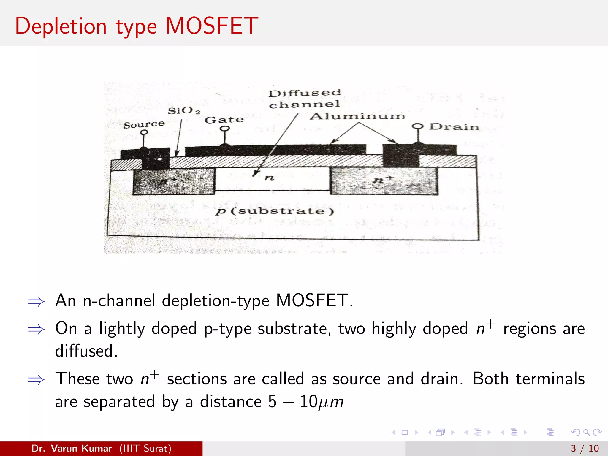
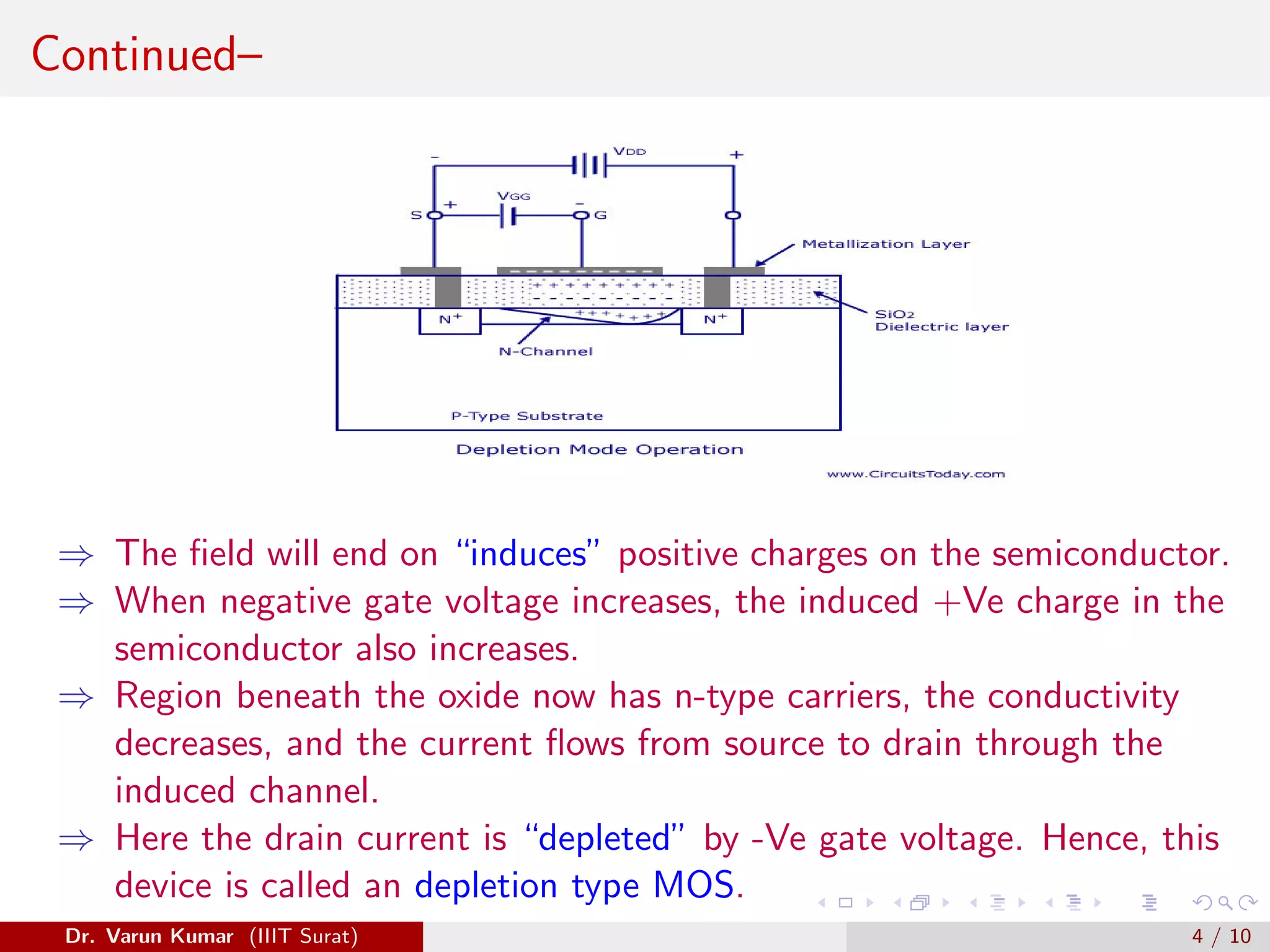
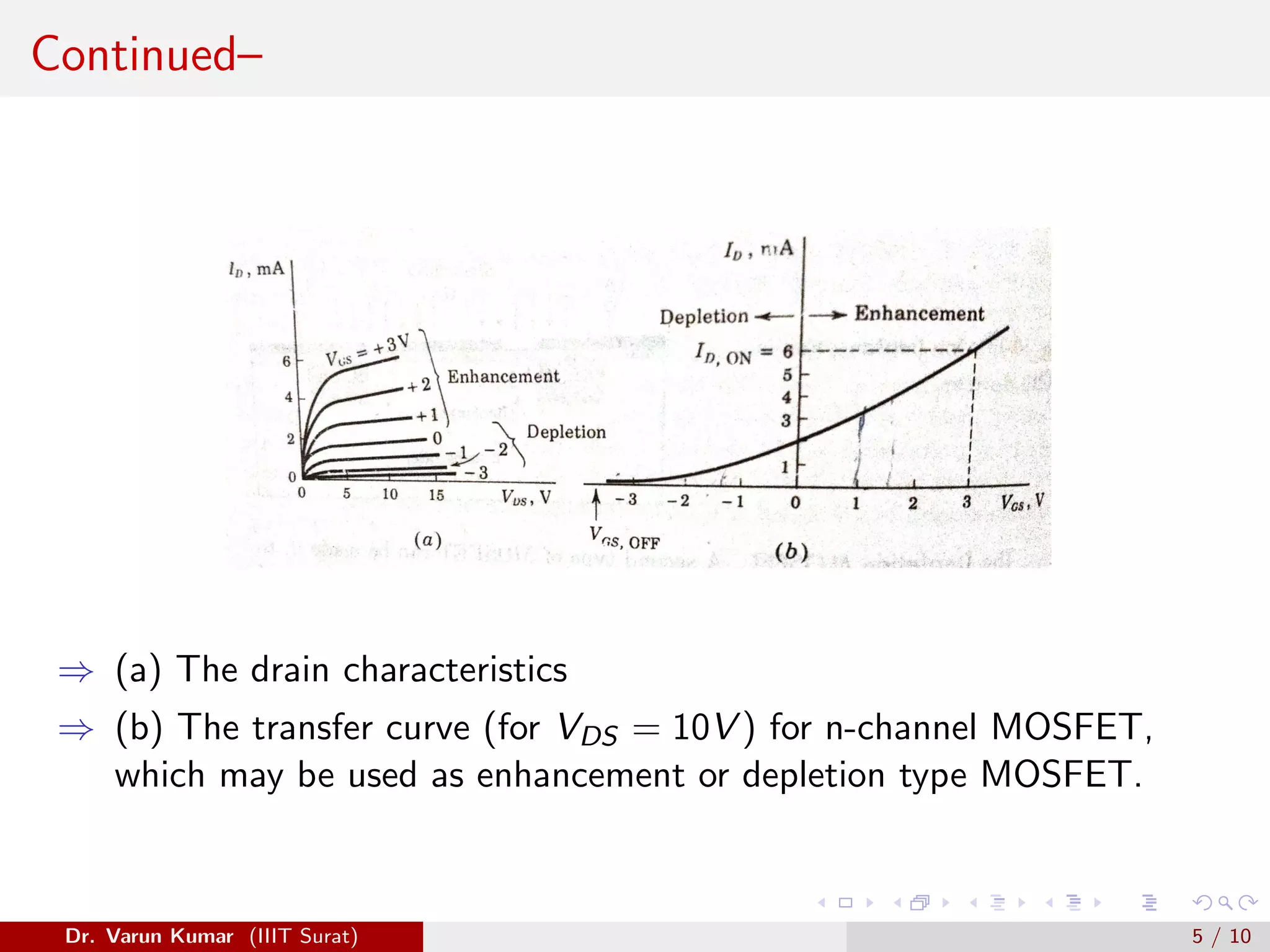
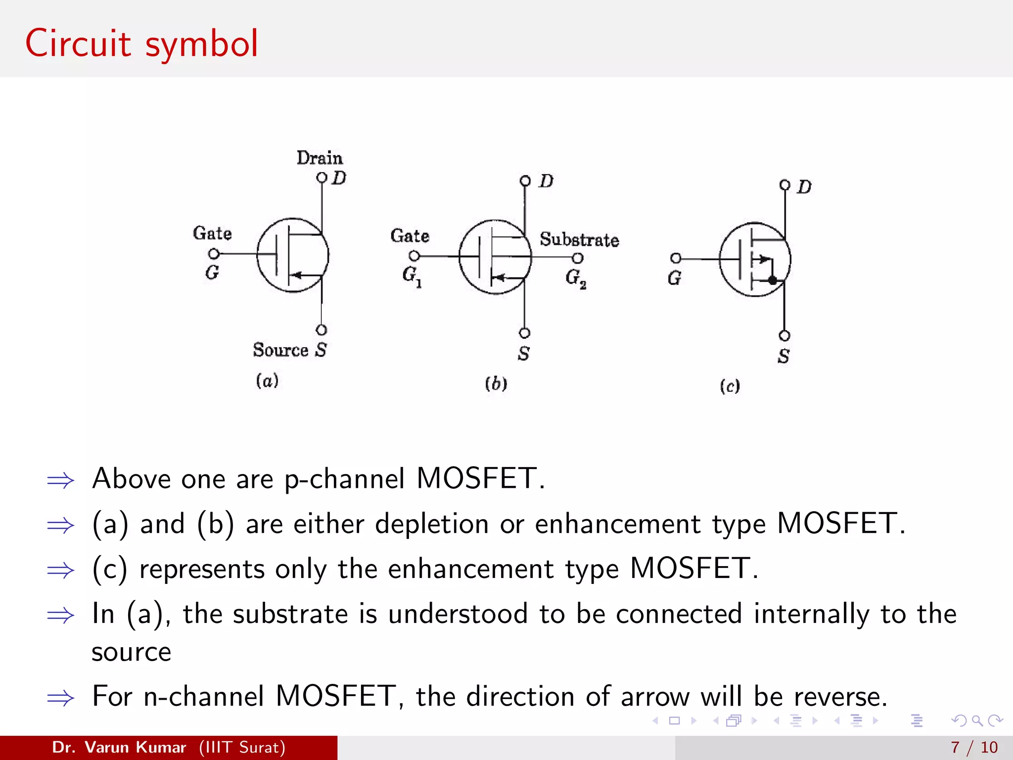
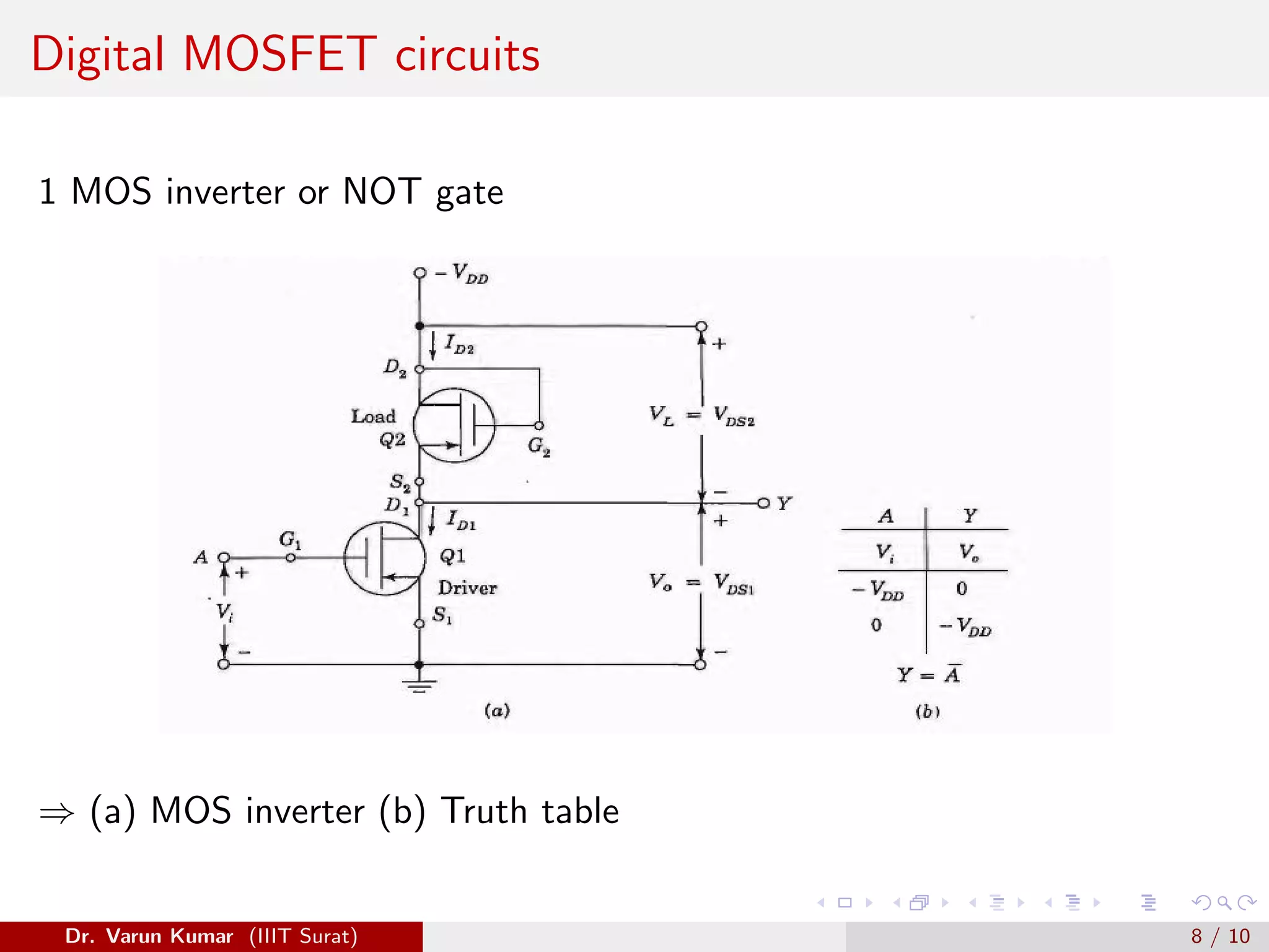
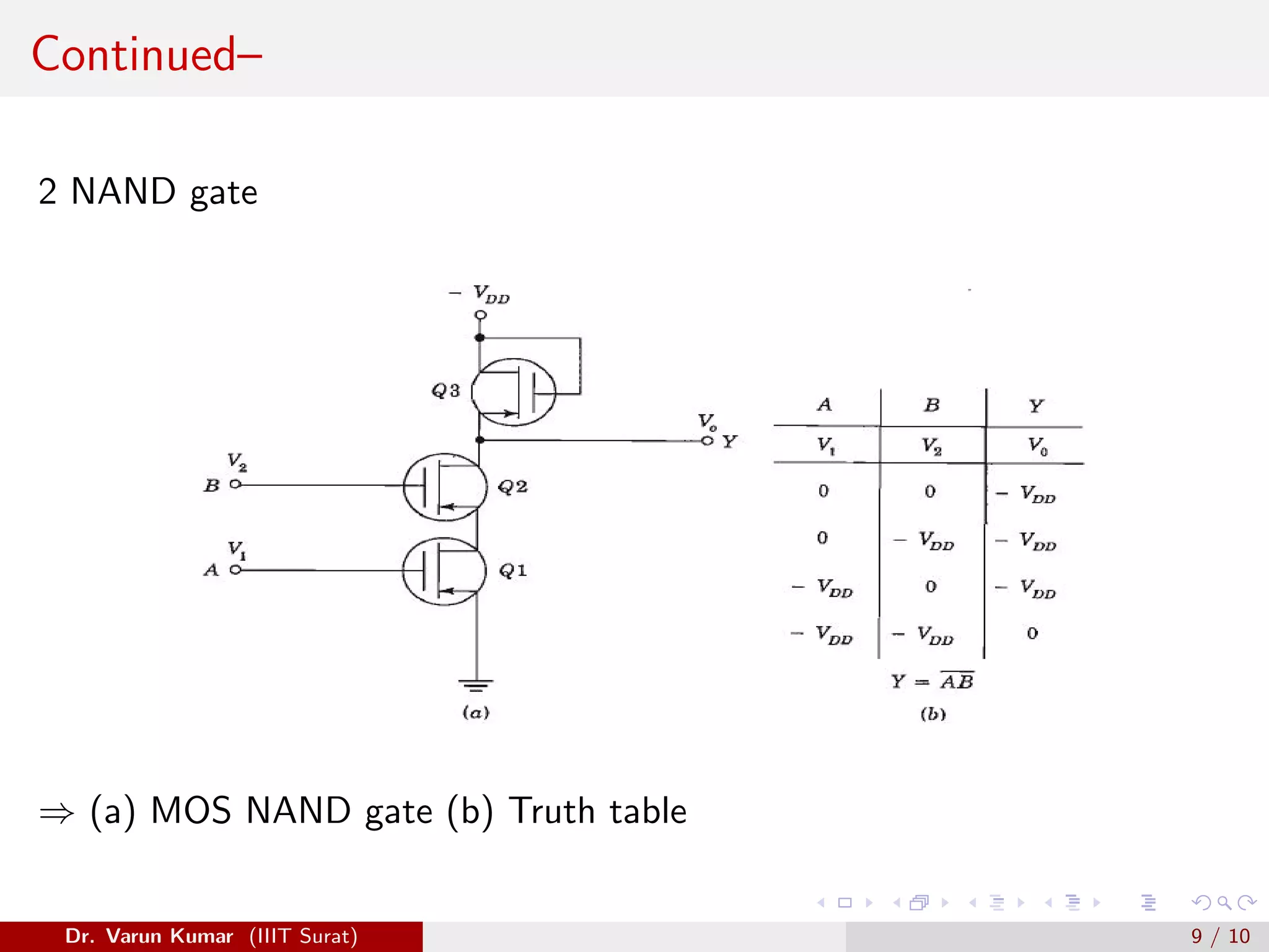
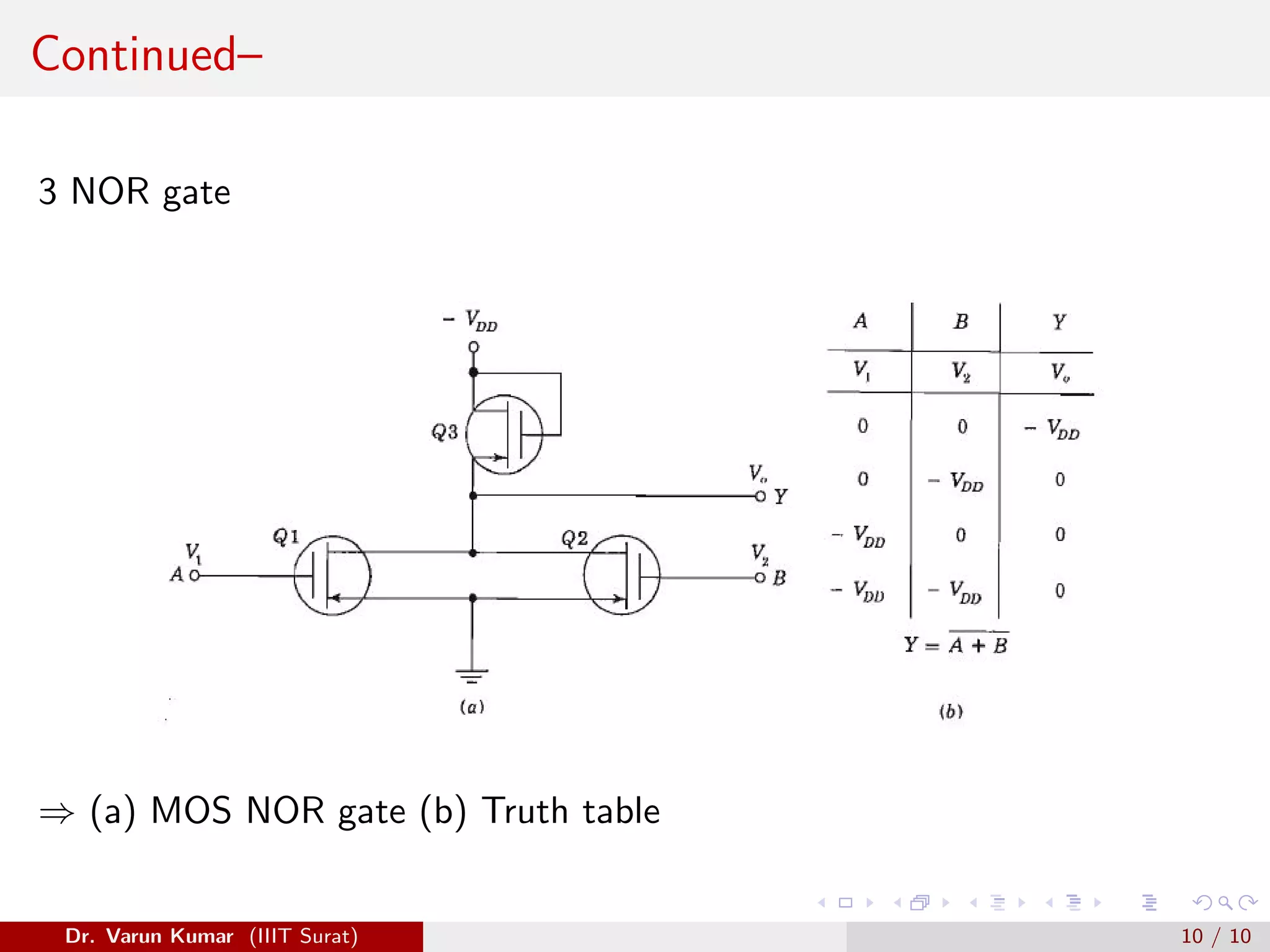
Depletion MOSFET and Digital MOSFET Circuits
Dr. Varun Kumar
Dr. Varun Kumar (IIIT Surat) 1 / 10
Outlines
1 Depletion MOSFET
2 Comparison of p-with n-channel FETs
3 Circuit symbol of MOSFET
4 Digital MOSFET circuits
Dr. Varun Kumar (IIIT Surat) 2 / 10
Depletion type MOSFET
⇒ An n-channel depletion-type MOSFET.
⇒ On a lightly doped p-type substrate, two highly doped n+ regions are
diffused.
⇒ These two n+ sections are called as source and drain. Both terminals
are separated by a distance 5 − 10µm
Dr. Varun Kumar (IIIT Surat) 3 / 10
Continued–
⇒ The field will end on “induces” positive charges on the semiconductor.
⇒ When negative gate voltage increases, the induced +Ve charge in the
semiconductor also increases.
⇒ Region beneath the oxide now has n-type carriers, the conductivity
decreases, and the current flows from source to drain through the
induced channel.
⇒ Here the drain current is “depleted” by -Ve gate voltage. Hence, this
device is called an depletion type MOS.
Dr. Varun Kumar (IIIT Surat) 4 / 10
Continued–
⇒ (a) The drain characteristics
⇒ (b) The transfer curve (for VDS = 10V ) for n-channel MOSFET,
which may be used as enhancement or depletion type MOSFET.
Dr. Varun Kumar (IIIT Surat) 5 / 10
Comparison of p-with n-channel FETs
⇒ p-channel enhancement FET is popular in MOS, due to its easier
production.
⇒ Most of the contaminant in MOS fabrications are mobile ions.
⇒ +Ve charge are trapped in oxide layer between gate and substrate.
⇒ The hole mobility in silicon at normal field is 500Cm2/V-s, whereas
electron mobility is 1300Cm2/V-s in
⇒ p-channel device will have more ON resistance on an equivalent
n-channel on same condition.
⇒ p-channel requires more than double area for maintaining the same
resistance.
Dr. Varun Kumar (IIIT Surat) 6 / 10
Circuit symbol
⇒ Above one are p-channel MOSFET.
⇒ (a) and (b) are either depletion or enhancement type MOSFET.
⇒ (c) represents only the enhancement type MOSFET.
⇒ In (a), the substrate is understood to be connected internally to the
source
⇒ For n-channel MOSFET, the direction of arrow will be reverse.
Dr. Varun Kumar (IIIT Surat) 7 / 10
Digital MOSFET circuits
1 MOS inverter or NOT gate
⇒ (a) MOS inverter (b) Truth table
Dr. Varun Kumar (IIIT Surat) 8 / 10
Continued–
2 NAND gate
⇒ (a) MOS NAND gate (b) Truth table
Dr. Varun Kumar (IIIT Surat) 9 / 10
Continued–
3 NOR gate
⇒ (a) MOS NOR gate (b) Truth table
Dr. Varun Kumar (IIIT Surat) 10 / 10

Depletion MOSFET and Digital MOSFET Circuits

  • 1.
    Depletion MOSFET andDigital MOSFET Circuits Dr. Varun Kumar Dr. Varun Kumar (IIIT Surat) 1 / 10
  • 2.
    Outlines 1 Depletion MOSFET 2Comparison of p-with n-channel FETs 3 Circuit symbol of MOSFET 4 Digital MOSFET circuits Dr. Varun Kumar (IIIT Surat) 2 / 10
  • 3.
    Depletion type MOSFET ⇒An n-channel depletion-type MOSFET. ⇒ On a lightly doped p-type substrate, two highly doped n+ regions are diffused. ⇒ These two n+ sections are called as source and drain. Both terminals are separated by a distance 5 − 10µm Dr. Varun Kumar (IIIT Surat) 3 / 10
  • 4.
    Continued– ⇒ The fieldwill end on “induces” positive charges on the semiconductor. ⇒ When negative gate voltage increases, the induced +Ve charge in the semiconductor also increases. ⇒ Region beneath the oxide now has n-type carriers, the conductivity decreases, and the current flows from source to drain through the induced channel. ⇒ Here the drain current is “depleted” by -Ve gate voltage. Hence, this device is called an depletion type MOS. Dr. Varun Kumar (IIIT Surat) 4 / 10
  • 5.
    Continued– ⇒ (a) Thedrain characteristics ⇒ (b) The transfer curve (for VDS = 10V ) for n-channel MOSFET, which may be used as enhancement or depletion type MOSFET. Dr. Varun Kumar (IIIT Surat) 5 / 10
  • 6.
    Comparison of p-withn-channel FETs ⇒ p-channel enhancement FET is popular in MOS, due to its easier production. ⇒ Most of the contaminant in MOS fabrications are mobile ions. ⇒ +Ve charge are trapped in oxide layer between gate and substrate. ⇒ The hole mobility in silicon at normal field is 500Cm2/V-s, whereas electron mobility is 1300Cm2/V-s in ⇒ p-channel device will have more ON resistance on an equivalent n-channel on same condition. ⇒ p-channel requires more than double area for maintaining the same resistance. Dr. Varun Kumar (IIIT Surat) 6 / 10
  • 7.
    Circuit symbol ⇒ Aboveone are p-channel MOSFET. ⇒ (a) and (b) are either depletion or enhancement type MOSFET. ⇒ (c) represents only the enhancement type MOSFET. ⇒ In (a), the substrate is understood to be connected internally to the source ⇒ For n-channel MOSFET, the direction of arrow will be reverse. Dr. Varun Kumar (IIIT Surat) 7 / 10
  • 8.
    Digital MOSFET circuits 1MOS inverter or NOT gate ⇒ (a) MOS inverter (b) Truth table Dr. Varun Kumar (IIIT Surat) 8 / 10
  • 9.
    Continued– 2 NAND gate ⇒(a) MOS NAND gate (b) Truth table Dr. Varun Kumar (IIIT Surat) 9 / 10
  • 10.
    Continued– 3 NOR gate ⇒(a) MOS NOR gate (b) Truth table Dr. Varun Kumar (IIIT Surat) 10 / 10