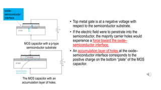
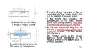
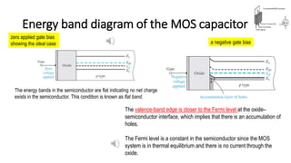
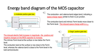
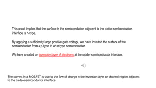
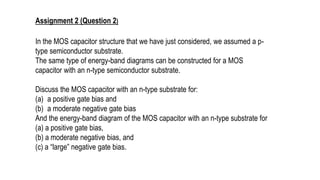
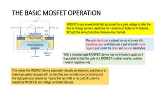
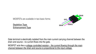
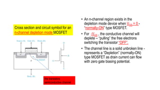
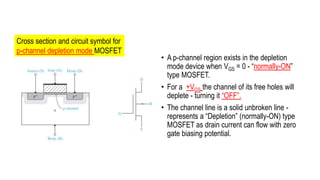
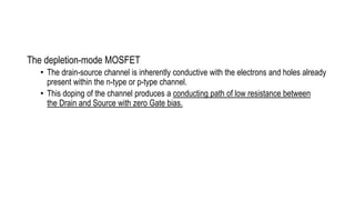
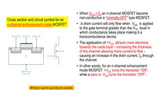
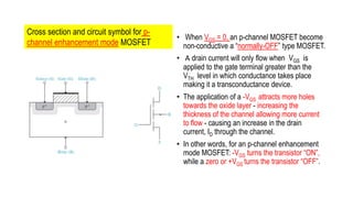
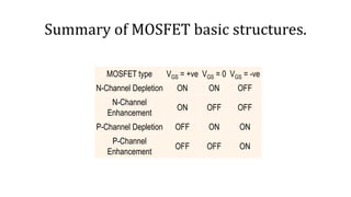
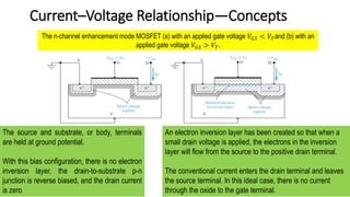
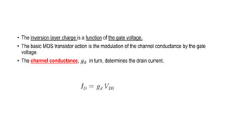
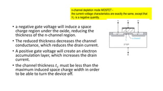
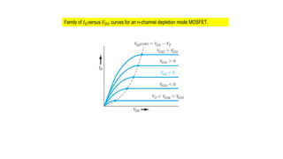
2. The basic MOS capacitor structure
• The heart of the MOSFET is the MOS capacitor.
• The parameter 𝑡𝑜𝑥 is the thickness of the oxide and ℰ𝑜𝑥 is the permittivity of
the oxide.
3. Basic MOS structure
• A parallel-plate capacitor with the top plate at a negative voltage with respect to the bottom
plate.
• An insulator material separates the two plates.
• With this bias, a negative charge exists on the top plate, a positive charge exists on the
bottom plate, and an electric field is induced between the two plates as shown.
• The capacitance per unit area for this geometry is:
where ε is the permittivity of the insulator and d is the distance
between the two plates.
4. The magnitude of the charge per unit area on either plate is:
The magnitude of the electric field is:
5. • Top metal gate is at a negative voltage with
respect to the semiconductor substrate.
• If the electric field were to penetrate into the
semiconductor, the majority carrier holes would
experience a force toward the oxide–
semiconductor interface.
• An accumulation layer of holes at the oxide–
semiconductor interface corresponds to the
positive charge on the bottom “plate” of the MOS
capacitor.
MOS capacitor with a p-type
semiconductor substrate
The MOS capacitor with an
accumulation layer of holes.
oxide–
semiconductor
interface.
6. • A positive charge now exists on the top
metal plate and the induced electric field
is in the opposite direction as shown.
• If the electric field penetrates the
semiconductor in this case, majority
carrier holes will experience a force away
from the oxide–semiconductor interface.
• As the holes are pushed away from the
interface, a negative space charge region
is created because of the fixed ionized
acceptor atoms.
• The negative charge in the induced
depletion region corresponds to the
negative charge on the bottom “plate” of
the MOS capacitor.
MOS capacitor in which the polarity
of the applied voltage is reversed.
The equilibrium distribution of charge in the
MOS capacitor with this applied voltage
7. Energy band diagram of the MOS capacitor
zero applied gate bias
showing the ideal case a negative gate bias
The energy bands in the semiconductor are flat indicating no net charge
exists in the semiconductor. This condition is known as flat band.
The valence-band edge is closer to the Fermi level at the oxide–
semiconductor interface, which implies that there is an accumulation of
holes.
The Fermi level is a constant in the semiconductor since the MOS
system is in thermal equilibrium and there is no current through the
oxide.
8. Energy band diagram of the MOS capacitor
a moderate positive gate bias The conduction- and valence-band edges bend, indicating a
space charge region similar to that in a pn junction.
The conduction band and intrinsic Fermi levels move closer to
the Fermi level. The induced space charge width is 𝑥𝑑.
a “large” positive gate bias
The induced electric field increase in magnitude - the positive and
negative charges on the MOS capacitor to increase.
The intrinsic Fermi level at the surface is now below the Fermi
level.
The conduction band at the surface is now close to the Fermi
level, whereas the valence band is close to the Fermi level in the
bulk semiconductor.
9. This result implies that the surface in the semiconductor adjacent to the oxide-semiconductor
interface is n-type.
By applying a sufficiently large positive gate voltage, we have inverted the surface of the
semiconductor from a p-type to an n-type semiconductor.
We have created an inversion layer of electrons at the oxide–semiconductor interface.
The current in a MOSFET is due to the flow of charge in the inversion layer or channel region adjacent
to the oxide–semiconductor interface.
10. In the MOS capacitor structure that we have just considered, we assumed a p-
type semiconductor substrate.
The same type of energy-band diagrams can be constructed for a MOS
capacitor with an n-type semiconductor substrate.
Discuss the MOS capacitor with an n-type substrate for:
(a) a positive gate bias and
(b) a moderate negative gate bias
And the energy-band diagram of the MOS capacitor with an n-type substrate for
(a) a positive gate bias,
(b) a moderate negative bias, and
(c) a “large” negative gate bias.
Assignment 2 (Question 2)
11. Depletion Layer Thickness
The energy-band diagram in the p-type
semiconductor, indicating surface potential.
The potential ∅𝑓𝑝 is the difference (in V) between 𝐸𝐹𝑖
and 𝐸𝐹 (in bulk SC) and is given by:
𝑁𝑎 is the acceptor doping concentration and 𝑛𝑖 is the
intrinsic carrier concentration.
The potential ∅𝑠 is called the surface potential; it
is the difference (in V) between 𝐸𝐹𝑖 measured in
the bulk semiconductor and 𝐸𝐹𝑖 measured at
the surface.
12. The space charge width can be written in a form similar to that of a one-sided pn
junction.
13. Now, for the case in which ∅𝑠 (surface)
= 2∅𝑝(𝑏𝑢𝑙𝑘);
The Fermi level at the surface is as far above the
intrinsic level as the Fermi level is below the
intrinsic level in the bulk semiconductor.
The electron concentration at the surface is the
same as the hole concentration in the bulk
material.
This condition is known as the threshold inversion
point.
14. The applied gate voltage creating this condition is
known as the threshold voltage.
If the gate voltage increases above this threshold
value, the conduction band will bend slightly closer
to the Fermi level, but the change in the
conduction band at the surface is now only a slight
function of gate voltage.
The surface potential may increase by a few (kTe)
volts, which will change the electron concentration
by orders of magnitude, but the space charge
width changes only slightly. In this case, then, the
space charge region has essentially reached a
maximum width.
15. The maximum space charge width, 𝑥𝑑𝑇, at this inversion transition point can be:
The same potential and maximum induced space charge region width occurs in an n-type substrate.
18. THE BASIC MOSFET OPERATION
The gate electrode is placed on top of a very thin
insulating layer and there are a pair of small n-type
regions just under the drain and source electrodes.
MOSFETs use an electrical field produced by a gate voltage to alter the
flow of charge carriers, electrons for n-channel or holes for P-channel,
through the semiconductive drain-source channel.
With a insulated gate MOSFET, device has no limitations apply so it
is possible to bias the gate of a MOSFET in either polarity, positive
(+ve) or negative (-ve).
This makes the MOSFET device especially valuable as electronic switches or to
make logic gates because with no bias they are normally non-conducting and
this high gate input resistance means that very little or no control current is
needed as MOSFETs are voltage controlled devices.
19. MOSFETs are available in two basic forms:
Depletion Type
Enhancement Type
Gate terminal is electrically isolated from the main current carrying channel between the
drain and source - no current flows into the gate.
MOSFET acts like a voltage controlled resistor– the current flowing through the main
channel between the drain and source is proportional to the input voltage.
20. • An n-channel region exists in the
depletion mode device when VGS = 0 -
“normally-ON” type MOSFET.
• For -VGS , the conductive channel will
deplete – “pulling” the free electrons
switching the transistor “OFF”.
• The channel line is a solid unbroken line -
represents a “Depletion” (normally-ON)
type MOSFET as drain current can flow
with zero gate biasing potential.
Cross section and circuit symbol for an
n-channel depletion mode MOSFET
the transistors
semiconductive channel
21. • A p-channel region exists in the depletion
mode device when VGS = 0 - “normally-ON”
type MOSFET.
• For a +VGS the channel of its free holes will
deplete - turning it “OFF”.
• The channel line is a solid unbroken line -
represents a “Depletion” (normally-ON) type
MOSFET as drain current can flow with zero
gate biasing potential.
Cross section and circuit symbol for
p-channel depletion mode MOSFET
22. The depletion-mode MOSFET
• The drain-source channel is inherently conductive with the electrons and holes already
present within the n-type or p-type channel.
• This doping of the channel produces a conducting path of low resistance between
the Drain and Source with zero Gate bias.
23. • When VGS = 0, an n-channel MOSFET become
non-conductive a “normally-OFF” type MOSFET.
• A drain current will only flow when VGS is applied
to the gate terminal greater than the VTH level in
which conductance takes place making it a
transconductance device.
• The application of +VGS attracts more electrons
towards the oxide layer - increasing the thickness
of the channel allowing more current to flow -
causing an increase in the drain current, ID through
the channel.
• In other words, for an n-channel enhancement
mode MOSFET: +VGS turns the transistor “ON”,
while a zero or -VGS turns the transistor “OFF”.
Cross section and circuit symbol for an
n-channel enhancement mode MOSFET
## Body is used for grounding the substrate.
24. • When VGS = 0, an p-channel MOSFET become
non-conductive a “normally-OFF” type MOSFET.
• A drain current will only flow when VGS is
applied to the gate terminal greater than the
VTH level in which conductance takes place
making it a transconductance device.
• The application of a -VGS attracts more holes
towards the oxide layer - increasing the
thickness of the channel allowing more current
to flow - causing an increase in the drain
current, ID through the channel.
• In other words, for an p-channel enhancement
mode MOSFET: -VGS turns the transistor “ON”,
while a zero or +VGS turns the transistor “OFF”.
Cross section and circuit symbol for p-
channel enhancement mode MOSFET
25. Enhancement-mode MOSFETs make excellent electronics switches due to their low “ON”
resistance and extremely high “OFF” resistance as well as their infinitely high input
resistance due to their isolated gate.
Enhancement-mode MOSFETs are used in integrated circuits to produce CMOS type Logic
Gates and power switching circuits in the form of as PMOS (P-channel) and NMOS (N-
channel) gates.
CMOS actually stands for Complementary MOS meaning that the logic device has both
PMOS and NMOS within its design.
26. Summary of MOSFET basic structures.
MOSFET type VGS = +ve VGS = 0 VGS = -ve
N-Channel Depletion ON ON OFF
N-Channel
Enhancement
ON OFF OFF
P-Channel Depletion OFF ON ON
P-Channel
Enhancement
OFF OFF ON
27. Current–Voltage Relationship—Concepts
The n-channel enhancement mode MOSFET (a) with an applied gate voltage 𝑉𝐺𝑆 < 𝑉𝑇and (b) with an
applied gate voltage 𝑉𝐺𝑆 > 𝑉𝑇.
The source and substrate, or body, terminals
are held at ground potential.
With this bias configuration, there is no electron
inversion layer, the drain-to-substrate p-n
junction is reverse biased, and the drain current
is zero
An electron inversion layer has been created so that when a
small drain voltage is applied, the electrons in the inversion
layer will flow from the source to the positive drain terminal.
The conventional current enters the drain terminal and leaves
the source terminal. In this ideal case, there is no current
through the oxide to the gate terminal.
28. • The inversion layer charge is a function of the gate voltage.
• The basic MOS transistor action is the modulation of the channel conductance by the gate
voltage.
• The channel conductance, 𝑔𝑑 in turn, determines the drain current.
29. • When 𝑉𝐺𝑆 < 𝑉𝑇, the drain current is zero.
• As 𝑉𝐺𝑆 becomes larger than 𝑉𝑇, channel
inversion charge density increases, which
increases the channel conductance.
• A larger value of 𝑔𝑑 produces a larger
initial slope of the 𝐼𝐷 versus 𝑉𝐷𝑆
characteristic.
𝐼𝐷 versus 𝑉𝐷𝑆 characteristics for small values
of 𝑉𝐷𝑆 at three 𝑉𝐺𝑆 voltages.
30. When VGS > VT and the applied VDS
voltage is small.
The IV graph similar to linear-ohmic
region occurrence.
Simplified MOS
structure for the
case when VGS >
VT.
Current–Voltage Relationship (𝑰𝑫 − 𝑽𝑫𝑺 concept)
31. • As the 𝑉𝐷𝑆↑, the voltage drop across
the oxide near the drain terminal ↓,
which means that the induced inversion
charge density near the drain also ↓.
• The incremental conductance of the
channel at the drain ↓, which then
means that the slope of the 𝐼𝐷versus
𝑉𝐷𝑆 curve will ↓.
32. • When 𝑉𝐷𝑆 increases to the point where the
potential drop across the oxide at the drain
terminal is equal to 𝑉𝑇, the induced inversion
charge density is zero at the drain terminal.
• At this point, the incremental conductance at
the drain is zero, which means that the slope of
the 𝐼𝐷versus 𝑉𝐷𝑆 curve is zero.
33. • When 𝑉𝐷𝑆 > 𝑉𝐷𝑆 (sat) value, the point in the
channel at which the inversion charge is just zero
moves toward the source terminal.
• If we assume that the change in channel length L is
small compared to the original length L, then the
drain current will be a constant for 𝑉𝐷𝑆 > 𝑉𝐷𝑆 (sat).
• The region of the 𝐼𝐷versus 𝑉𝐷𝑆 characteristic is
referred to as the saturation region.
34. • When 𝑉𝐺𝑆 changes, the 𝐼𝐷versus 𝑉𝐷𝑆 curve will change.
• If 𝑉𝐺𝑆 increases, the initial slope of 𝐼𝐷versus 𝑉𝐷𝑆increases.
• Knowing that the value of 𝑉𝐷𝑆 (sat) is a function of 𝑉𝐺𝑆, we can generate the family of
curves for this n-channel enhancement mode MOSFET.
35. • In the nonsaturation region;
• When the transistor is biased in the saturation region, the ideal
current–voltage relation is given by;
36. For 𝑉𝐷𝑆 > 𝑉𝐷𝑆 (sat) the ideal drain current is a constant and is equal to;
41. Assignment 2 (QUESTION 3)
An ideal n-channel MOSFET has the following parameters:
𝑊 = 30 μm 𝐿 = 2 μm 𝐶𝑜𝑥 = 350 Å
𝑉𝑇 = +0.80 𝑉 𝜇𝑛 = 450 cm2
/Vs
(a) Plot 𝐼𝐷 versus 𝑉𝐷𝑆 for 0 ≤ 𝑉𝐷𝑆 ≤ 5 V, for 𝑉𝐺𝑆 = 0, 1, 2, 3, 4, and 5 V and indicate the
𝑉𝐷𝑆 (sat) point of each curve.
(b) Plot 𝐼𝐷 versus 𝑉𝐺𝑆 for 𝑉𝐷𝑆 = 0.1 V and for 0 ≤ 𝑉𝐺𝑆 ≤ 5 V.
An ideal p-channel MOSFET has the following parameters:
𝑊 = 15 μm 𝐿 = 1.5 μm 𝐶𝑜𝑥 = 350 Å
42. Assignment 2 (QUESTION 4)
(a) Plot 𝐼𝐷 versus 𝑉𝐷𝑆 for 0 ≤ 𝑉𝐷𝑆 ≤ 5 V, for 𝑉𝐺𝑆 = 0, 1, 2, 3, 4, and 5 V and indicate the
𝑉𝐷𝑆 (sat) point of each curve.
(b) Plot 𝐼𝐷 versus 𝑉𝐺𝑆 for 𝑉𝐷𝑆 = 0.1 V and for 0 ≤ 𝑉𝐺𝑆 ≤ 5 V.
An ideal p-channel MOSFET has the following parameters:
𝑊 = 15 μm 𝐿 = 1.5 μm 𝐶𝑜𝑥 = 350 Å
𝑉𝑇 = − 0.80 𝑉 𝜇𝑝 = 300 cm2
/Vs
(a) Plot 𝐼𝐷 versus 𝑉𝐷𝑆 for 0 ≤ 𝑉𝐷𝑆 ≤ 5 V, for 𝑉𝐺𝑆 = 0, 1, 2, 3, 4, and 5 V and indicate the
𝑉𝐷𝑆 (sat) point of each curve.
(b) Plot 𝐼𝐷 versus 𝑉𝐺𝑆 for 𝑉𝐷𝑆 = 0.1 𝑉 and for 0 ≤ 𝑉𝐺𝑆 ≤ 5 V.
43. • a negative gate voltage will induce a space
charge region under the oxide, reducing the
thickness of the n-channel region.
• The reduced thickness decreases the channel
conductance, which reduces the drain current.
• A positive gate voltage will create an electron
accumulation layer, which increases the drain
current.
• the channel thickness 𝑡𝑐 must be less than the
maximum induced space charge width in order
to be able to turn the device off.
n-channel depletion mode MOSFET -
the current–voltage characteristics are exactly the same, except that
𝑉𝑇 is a negative quantity.
We expect the induced electric field to increase in magnitude and the corresponding positive and negative charges on the MOS capacitor to increase.
A larger negative charge in the MOS capacitor implies a larger induced space charge region and more band bending.
Deplete – reduce, exhaust, diminish
If the channel line is shown as a dotted or broken line, then it represents an “Enhancement” (normally-OFF) type MOSFET as zero drain current flows with zero gate potential.
The direction of the arrow pointing to this channel line indicates whether the conductive channel is a P-type or an N-type semiconductor device.
It contains p-type source and drain regions in an n-type substrate. The inversion layer is formed when holes are attracted to the interface by a negative gate voltage. While the holes still flow from source to drain, they result in a negative drain current.
In this case, electrons enter the channel at the source, travel through the channel toward the drain, and then, at the point where the charge goes to zero, the electrons are injected into the space charge region where they are swept by the E-field to the drain contact.