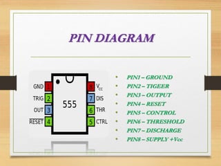
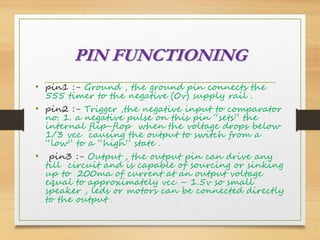
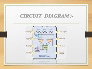
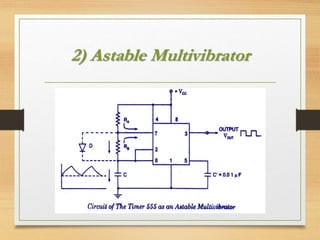
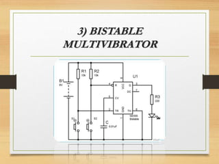
GOVERNMENT ENGINEERING
COLLEGE, GANDHINAGAR
Submitted by:-
Tanish Gupta{150130117029}
ANALOG SIGNAL PROCESSING
TOPIC :-
555
TIMER
CONTENTS :-
• INTRODUCTION
• PIN DIAGRAM
• TYPES
• WORKING
INTRODUCTION
• 555 timer is and integrated circuit.
• It is used in variety of timer ,pulse
generator ,oscillator .
• It is used to provide delays in
oscillator circuit .
• It was designed in 1971 by hans r.
camenzind .
INTRODUCTION
• NE-555 is used at
commercial range of 0˚c to
70˚c .
• SE-555 is used at military
purpose , it range of -55˚c
to 125˚c .
PIN DIAGRAM
• PIN1 – GROUND
• PIN2 – TIGEER
• PIN3 – OUTPUT
• PIN4 – RESET
• PIN5 – CONTROL
• PIN6 – THRESHOLD
• PIN7 – DISCHARGE
• PIN8 – SUPPLY +Vcc
PIN FUNCTIONING
• pin1 :- Ground , the ground pin connects the
555 timer to the negative (0v) supply rail .
• pin2 :- Trigger ,the negative input to comparator
no. 1. a negative pulse on this pin “sets” the
internal flip-flop when the voltage drops below
1/3 vcc causing the output to switch from a
“low” to a “high” state .
• pin3 :- Output , the output pin can drive any
till circuit and is capable of sourcing or sinking
up to 200ma of current at an output voltage
equal to approximately vcc – 1.5v so small
speaker , leds or motors can be connected directly
to the output .
• pin4 :- Reset , this pin is used to “reset” the internal
flip-flop controlling the state of the output ,pin3 . this
is an active-low input and is generally connected to a
logic “1” level when not used to prevent any unwanted
resetting of the output .
• pin5 :- Control voltage , this pin controls the timings
of the 555 by overriding the 2/3 vcc level of the
voltage divider network . by applying a voltage to this
pin the width of the output signal can be varied
independently of the rc timing network . when not used
it is connected to ground via a 10nf capacitor to
eliminate any noise .
• pin6 :- Threshold , the positve input of comparater no.
2 . this pin is used to reset the flip-flop when the
voltage applied to it exceeds 2/3 vcc causing the
output to switch from “high” to “low” state . this pin
connects directly to the rc timing circuit .
• pin7 :- Discharge , the discharge pin
isconnected directly to the collector of an
internal npn transistor which is used to
“discharge” the timing capacitor to ground
when the output at pin 3 switches “low” .
• pin8 :- Supply +vcc , this is he power supply
pin and for general purpose ttl 555 timers is
between 4.5v and 15v .
CIRCUIT DIAGRAM :-
TYPES :-
• 1) MONOSTABLE
MULTIVAIBRATOR
• 2) ASTABLE
MULTIVAIBRATOR
• 3) BISTABLE
MULTIVAIBRATOR
1) MONOSTABLE
MULTIVAIBRATOR
WORKING :-
• According to the fig. , initially when the
output is low , that is , circuit is in the stable
state , transistor Q1 is on and the capacitor C
is shorted out to ground . However , upon
application of a negative trigger pulse to pin 2
, transistor Q1 is turned off , which releases
the short circuit the external capacitor C
and driver the output is high .
• The capacitor C now starts charging up toward
Vcc through Ra.
• However , when the voltage across the
capacitor equal 2/3 Vcc , comparator 1’s
output switches from low to high ,which in
turn drives the output to its low state via the
output of the flip-flop .
• At the same time , the output of the flip-flop
turns transistor Q1 on and hence capacitor C
rapidly discharges through the transistor .
• The output of the monostable remains low
until a trigger pulse is again applied . The
cycle repeats .
• The time during which the output remains
high is given by Tp = 1.1RC seconds .
2) Astable Multivibrator
WORKING :-
• Fig. shows the 555 timer is connected as an astable
multivibrator . Initially , when the output is high
, capacitor C starts charging towards Vcc through
Ra and Rb .
• However , as soon as voltage across the capacitor
equal 2/3 Vcc , comparator 1 triggers the flip-
flop , and the output switches low .
• Now capacitor C starts discharge through Rb and
transistor Q1 .
• When the voltage across C equals 1/3 Vcc ,
comparator 2’s output triggers the flip-flop and the
output goes high .
• The cycle repeats .
FOMULAS :-
• CHARING TIME
Tc = 0.69(Ra +Rb)C
• DISCHARGING TIME
Td = 0.69(Rb)C
• TOTAL PERIOD
T = Tc +Td
• FREQUENCY
f = 1/T = 1.45/(Ra + 2Rb)C
• DUTY CYCLE
D = Tc/T = Ra + Rb/Ra + 2Rb
3) BISTABLE
MULTIVIBRATOR
APPLICATIONS OF
MONOSTABLE
MULTIVIBRATOR :-
•1) FREQUENCY
DIVIDER
•2) PULSE
STRETCHER
A) FREQUENCY
DIVIDER B) PULSE STRETCHER
APPLICATIONS OF ASTABLE
MULTIVIBRATOR
•1) SQUARE – WAVE
OSCILLATOR
•2) FREE- RUNNING
RAM GENERATOR
A) SQUARE –WAVE
OSCILLATOR
B) FREE- RUNNING RAMP
GENERATOR
THANK
YOU

555 Timer (detailed presentation)

  • 1.
  • 2.
  • 3.
  • 4.
    CONTENTS :- • INTRODUCTION •PIN DIAGRAM • TYPES • WORKING
  • 5.
    INTRODUCTION • 555 timeris and integrated circuit. • It is used in variety of timer ,pulse generator ,oscillator . • It is used to provide delays in oscillator circuit . • It was designed in 1971 by hans r. camenzind .
  • 6.
    INTRODUCTION • NE-555 isused at commercial range of 0˚c to 70˚c . • SE-555 is used at military purpose , it range of -55˚c to 125˚c .
  • 7.
    PIN DIAGRAM • PIN1– GROUND • PIN2 – TIGEER • PIN3 – OUTPUT • PIN4 – RESET • PIN5 – CONTROL • PIN6 – THRESHOLD • PIN7 – DISCHARGE • PIN8 – SUPPLY +Vcc
  • 8.
    PIN FUNCTIONING • pin1:- Ground , the ground pin connects the 555 timer to the negative (0v) supply rail . • pin2 :- Trigger ,the negative input to comparator no. 1. a negative pulse on this pin “sets” the internal flip-flop when the voltage drops below 1/3 vcc causing the output to switch from a “low” to a “high” state . • pin3 :- Output , the output pin can drive any till circuit and is capable of sourcing or sinking up to 200ma of current at an output voltage equal to approximately vcc – 1.5v so small speaker , leds or motors can be connected directly to the output .
  • 9.
    • pin4 :-Reset , this pin is used to “reset” the internal flip-flop controlling the state of the output ,pin3 . this is an active-low input and is generally connected to a logic “1” level when not used to prevent any unwanted resetting of the output . • pin5 :- Control voltage , this pin controls the timings of the 555 by overriding the 2/3 vcc level of the voltage divider network . by applying a voltage to this pin the width of the output signal can be varied independently of the rc timing network . when not used it is connected to ground via a 10nf capacitor to eliminate any noise . • pin6 :- Threshold , the positve input of comparater no. 2 . this pin is used to reset the flip-flop when the voltage applied to it exceeds 2/3 vcc causing the output to switch from “high” to “low” state . this pin connects directly to the rc timing circuit .
  • 10.
    • pin7 :-Discharge , the discharge pin isconnected directly to the collector of an internal npn transistor which is used to “discharge” the timing capacitor to ground when the output at pin 3 switches “low” . • pin8 :- Supply +vcc , this is he power supply pin and for general purpose ttl 555 timers is between 4.5v and 15v .
  • 11.
  • 12.
    TYPES :- • 1)MONOSTABLE MULTIVAIBRATOR • 2) ASTABLE MULTIVAIBRATOR • 3) BISTABLE MULTIVAIBRATOR
  • 13.
  • 14.
    WORKING :- • Accordingto the fig. , initially when the output is low , that is , circuit is in the stable state , transistor Q1 is on and the capacitor C is shorted out to ground . However , upon application of a negative trigger pulse to pin 2 , transistor Q1 is turned off , which releases the short circuit the external capacitor C and driver the output is high . • The capacitor C now starts charging up toward Vcc through Ra.
  • 15.
    • However ,when the voltage across the capacitor equal 2/3 Vcc , comparator 1’s output switches from low to high ,which in turn drives the output to its low state via the output of the flip-flop . • At the same time , the output of the flip-flop turns transistor Q1 on and hence capacitor C rapidly discharges through the transistor . • The output of the monostable remains low until a trigger pulse is again applied . The cycle repeats . • The time during which the output remains high is given by Tp = 1.1RC seconds .
  • 16.
  • 17.
    WORKING :- • Fig.shows the 555 timer is connected as an astable multivibrator . Initially , when the output is high , capacitor C starts charging towards Vcc through Ra and Rb . • However , as soon as voltage across the capacitor equal 2/3 Vcc , comparator 1 triggers the flip- flop , and the output switches low . • Now capacitor C starts discharge through Rb and transistor Q1 . • When the voltage across C equals 1/3 Vcc , comparator 2’s output triggers the flip-flop and the output goes high . • The cycle repeats .
  • 18.
    FOMULAS :- • CHARINGTIME Tc = 0.69(Ra +Rb)C • DISCHARGING TIME Td = 0.69(Rb)C • TOTAL PERIOD T = Tc +Td • FREQUENCY f = 1/T = 1.45/(Ra + 2Rb)C • DUTY CYCLE D = Tc/T = Ra + Rb/Ra + 2Rb
  • 19.
  • 20.
    APPLICATIONS OF MONOSTABLE MULTIVIBRATOR :- •1)FREQUENCY DIVIDER •2) PULSE STRETCHER
  • 21.
    A) FREQUENCY DIVIDER B)PULSE STRETCHER
  • 22.
    APPLICATIONS OF ASTABLE MULTIVIBRATOR •1)SQUARE – WAVE OSCILLATOR •2) FREE- RUNNING RAM GENERATOR
  • 23.
    A) SQUARE –WAVE OSCILLATOR B)FREE- RUNNING RAMP GENERATOR
  • 24.