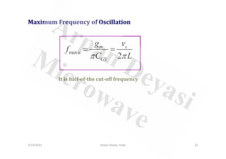
![Cut-off Frequency
2 4
m s
co
GS
g v
f
C L
π π
= =
2/19/2021 Arpan Deyasi, India 21
Cut-off frequency depends on
[i] gate length
[ii] saturated drift velocity](https://image.slidesharecdn.com/mesfet-210218192904/85/MESFET-21-320.jpg)
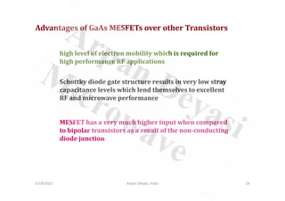

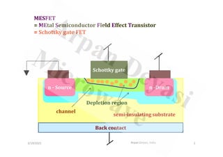
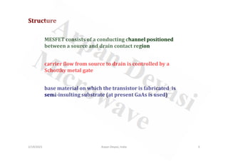
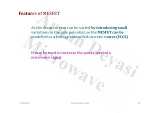
1) MESFET stands for Metal-Semiconductor Field Effect Transistor and consists of a conducting channel between a source and drain contact that is controlled by a Schottky metal gate. 2) The I-V characteristics of a MESFET can be modeled as a voltage-controlled current source where the drain current is varied by small changes in the gate potential. 3) MESFETs have advantages over other transistors for RF applications due to their high electron mobility, low stray capacitance from the Schottky gate, and negative temperature coefficient.


