Downloaded 206 times
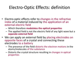
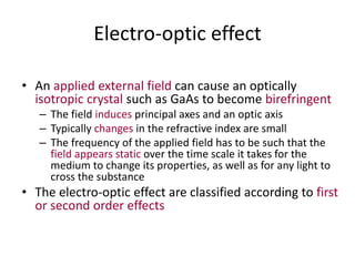
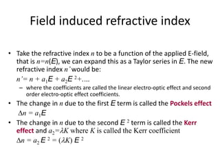

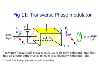
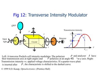
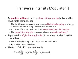
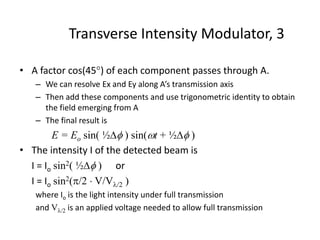
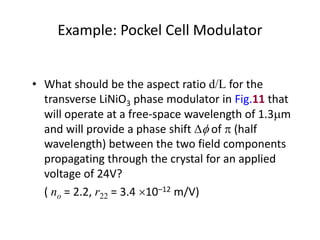
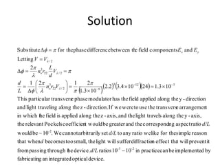
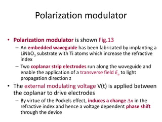
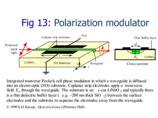
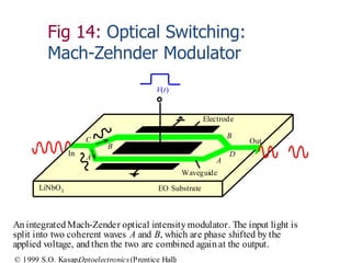

This document defines electro-optic effects and describes how an external electric field can induce changes in the refractive index of a material, modulating its optical properties. It discusses the Pockels effect specifically, where a linear change in refractive index occurs due to an applied electric field. This effect can be used to build integrated optical modulators and switches, such as a transverse Pockels cell that inserts a phase difference between orthogonal field components, acting as a polarization modulator. The phase difference can be converted to an intensity variation using an interferometer such as a Mach-Zehnder configuration.