Downloaded 244 times


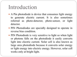
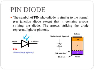
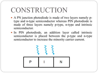
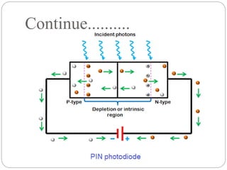


The document discusses the PIN photodiode, including its construction, working, advantages, disadvantages, and applications. A PIN photodiode consists of a p-type semiconductor, intrinsic semiconductor, and n-type semiconductor layer. When light hits the photodiode, electron-hole pairs are generated in the intrinsic region. Under reverse bias, the electrons and holes move to the n-region and p-region respectively, generating an electric current proportional to the light intensity. PIN photodiodes have advantages like wide bandwidth, high speed, and low capacitance compared to PN junction photodiodes. They are used in applications such as optical communications, medical equipment, and light detection.


