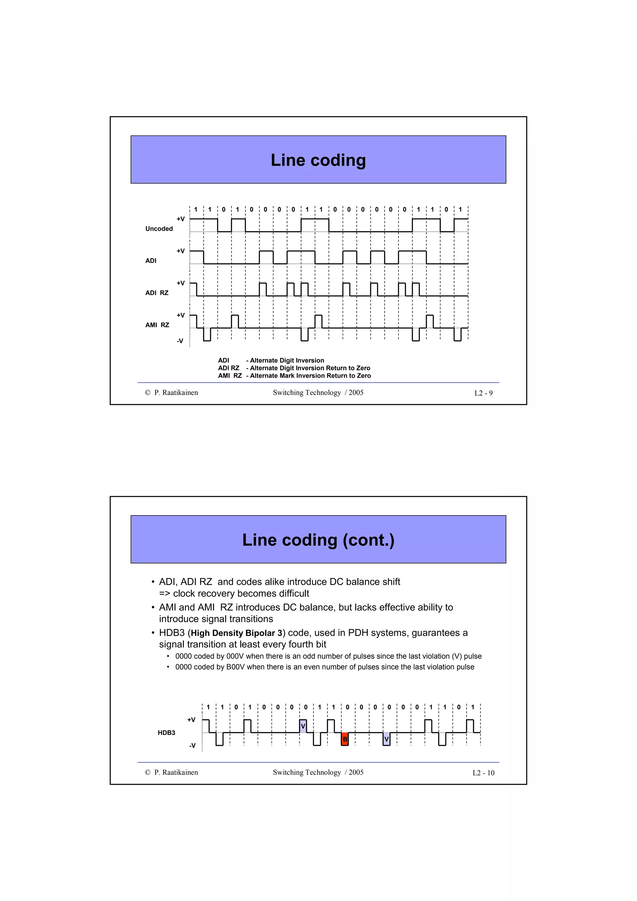
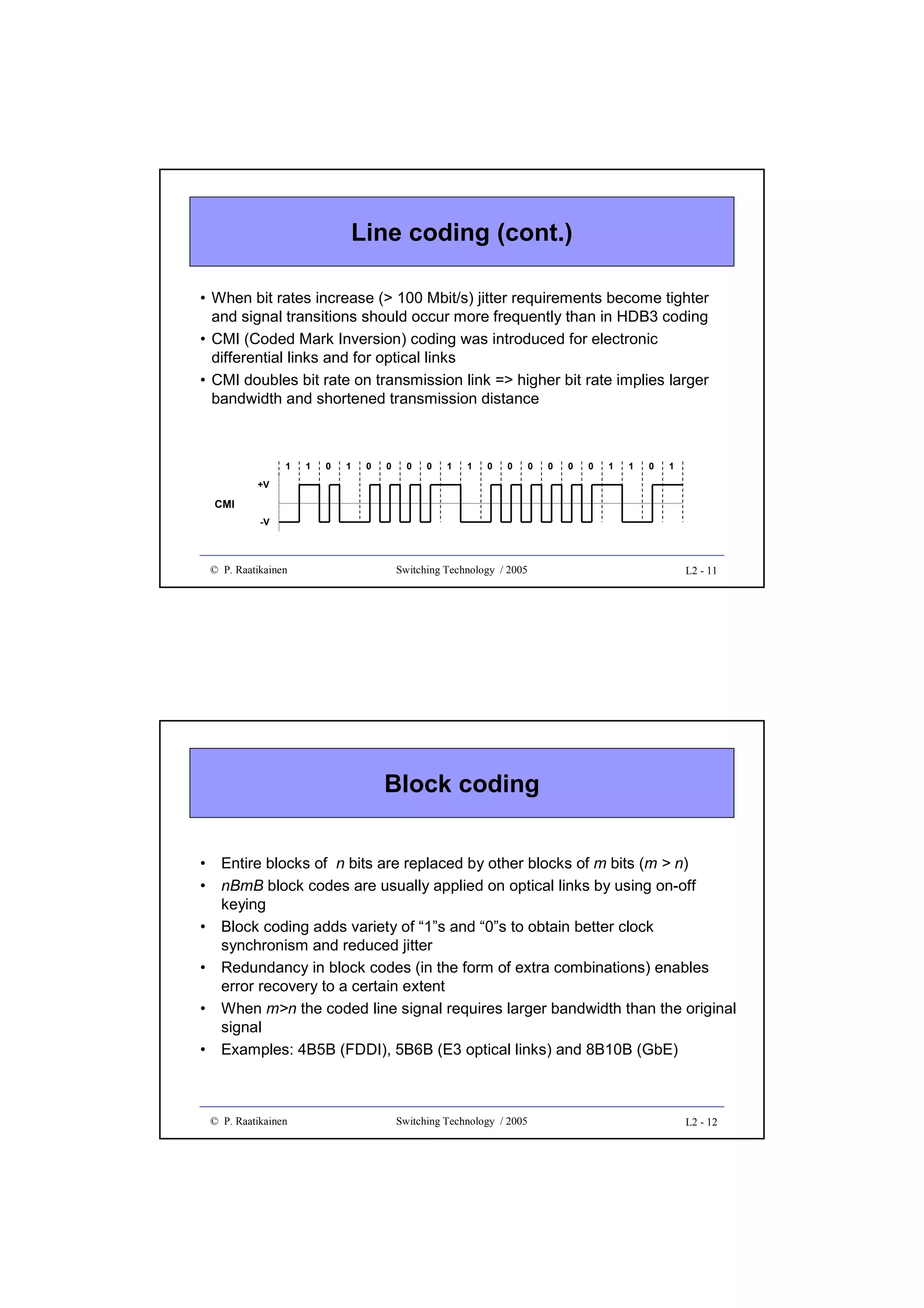
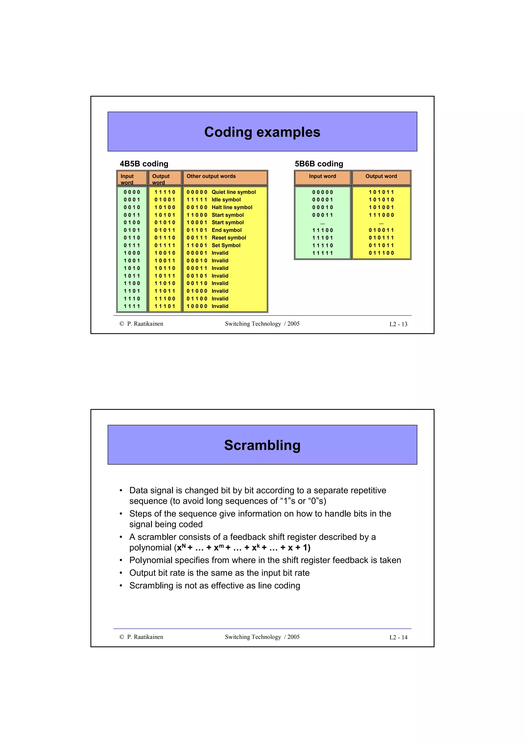
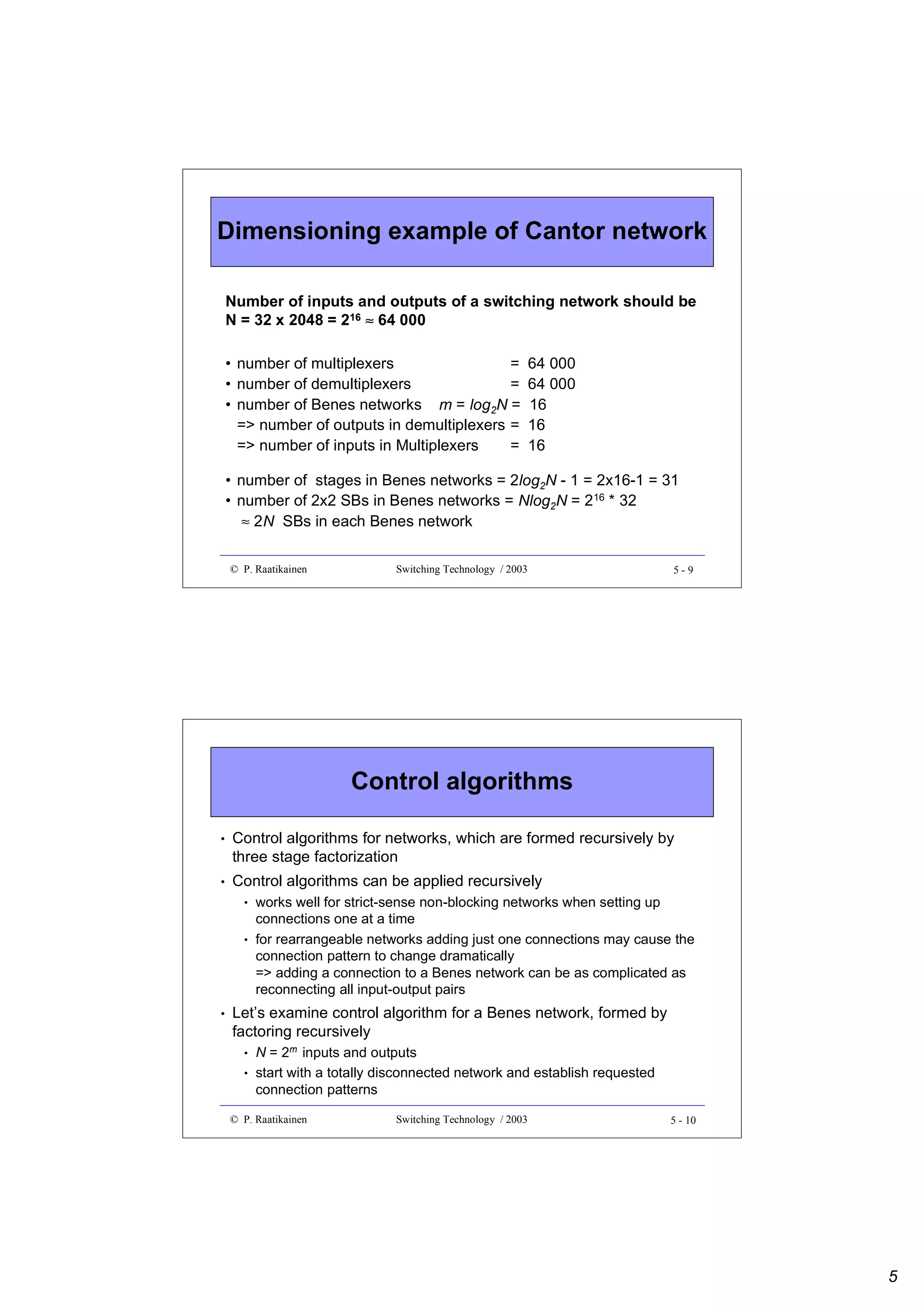
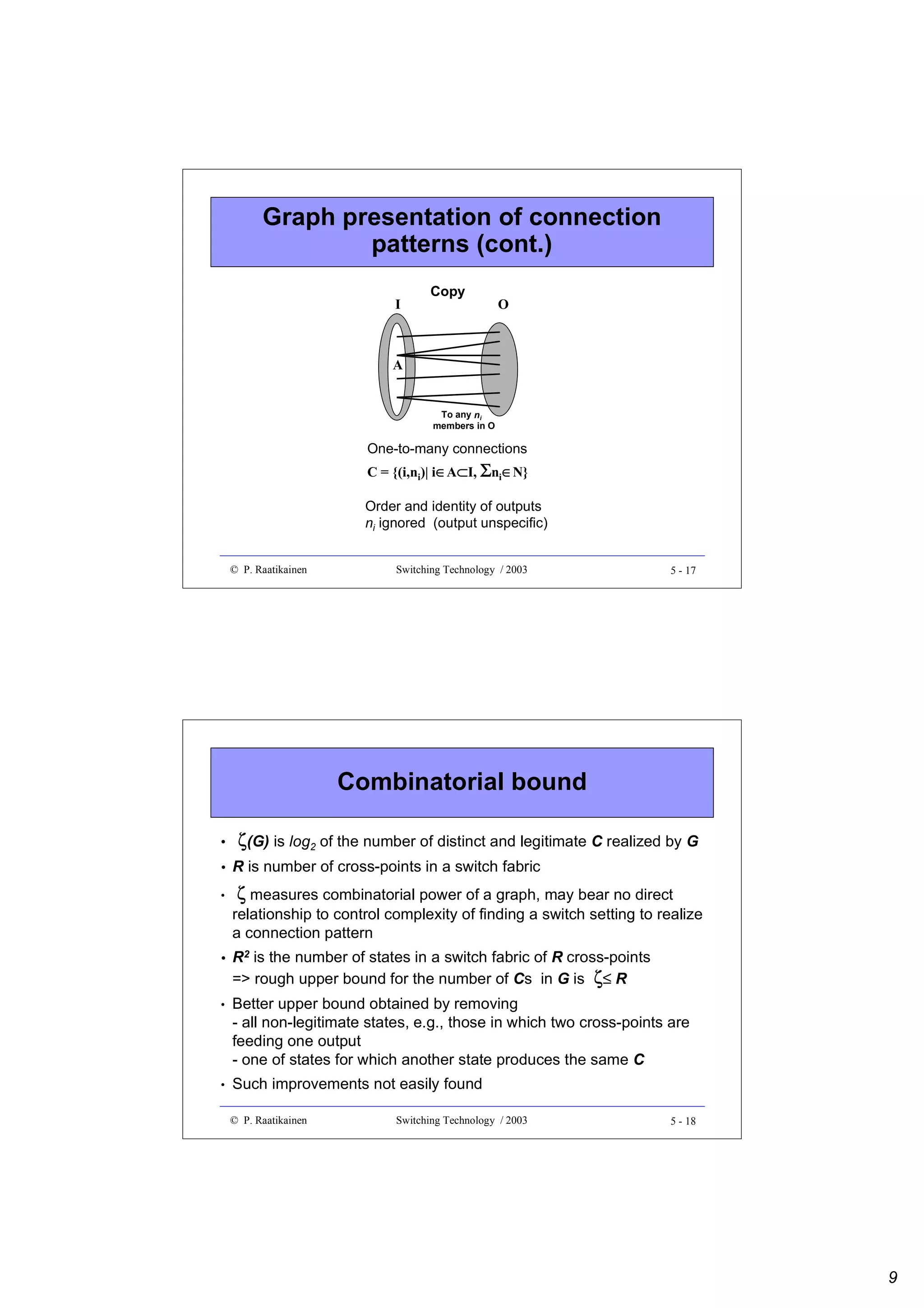
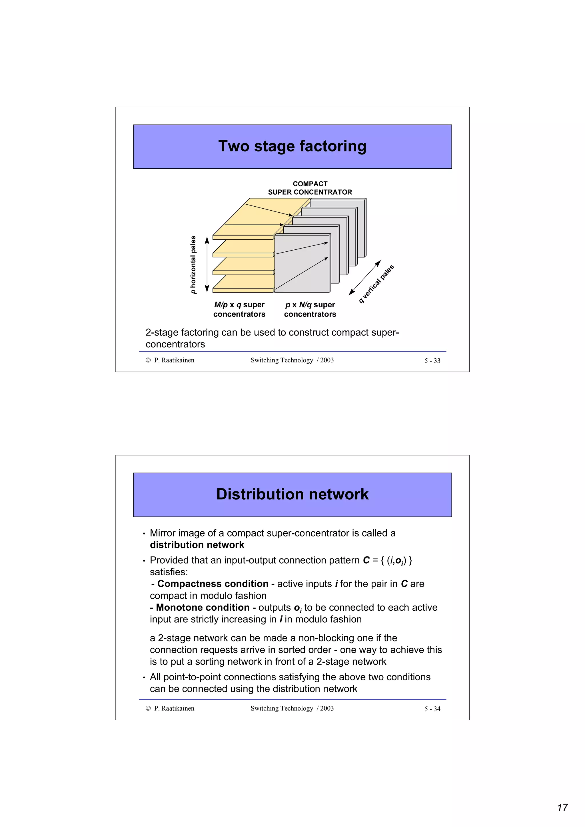
Downloaded 157 times
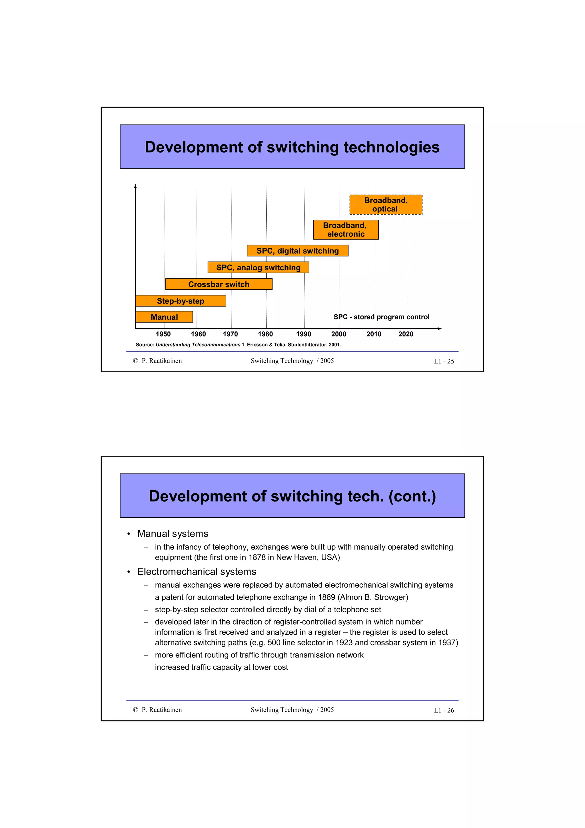

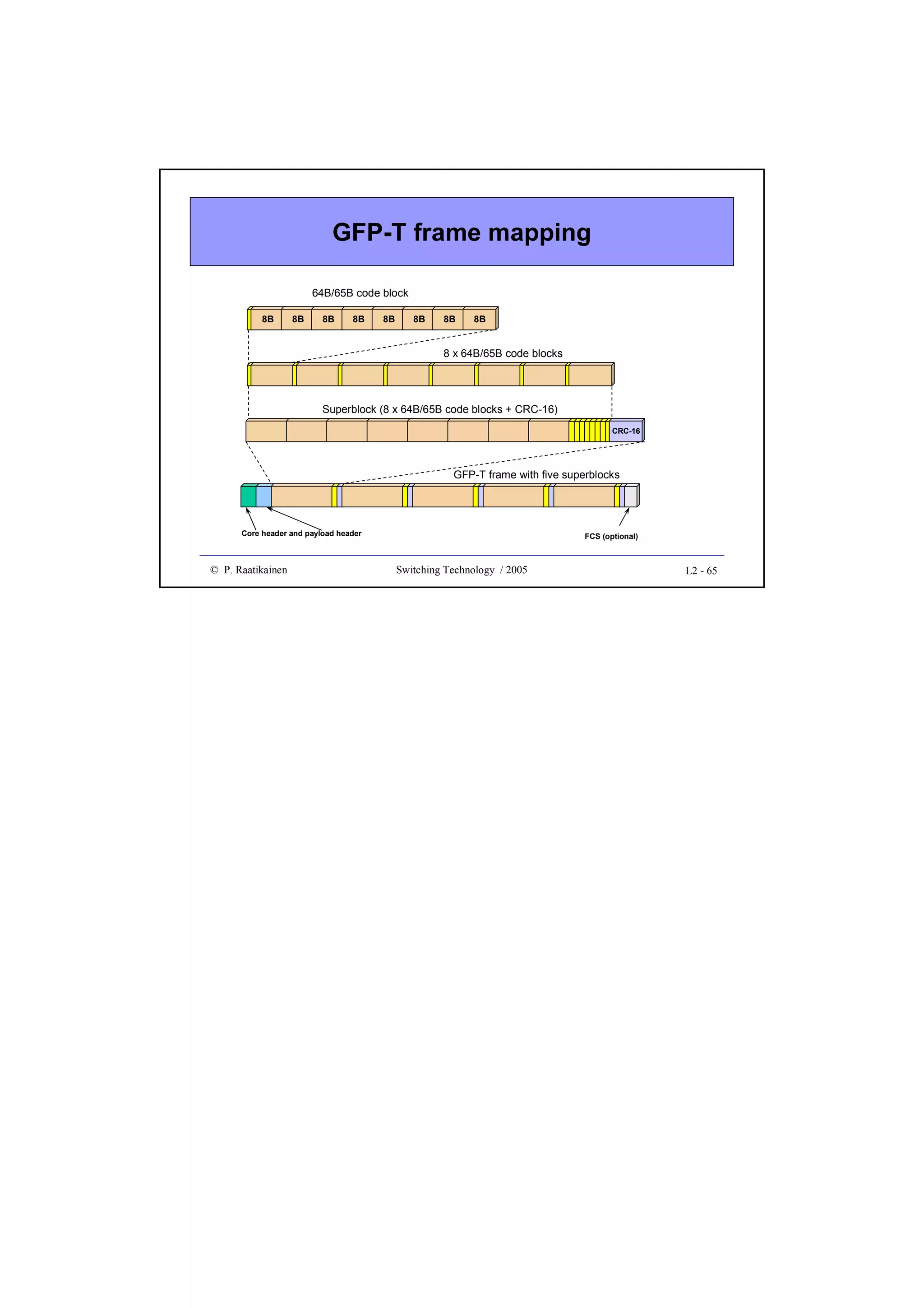
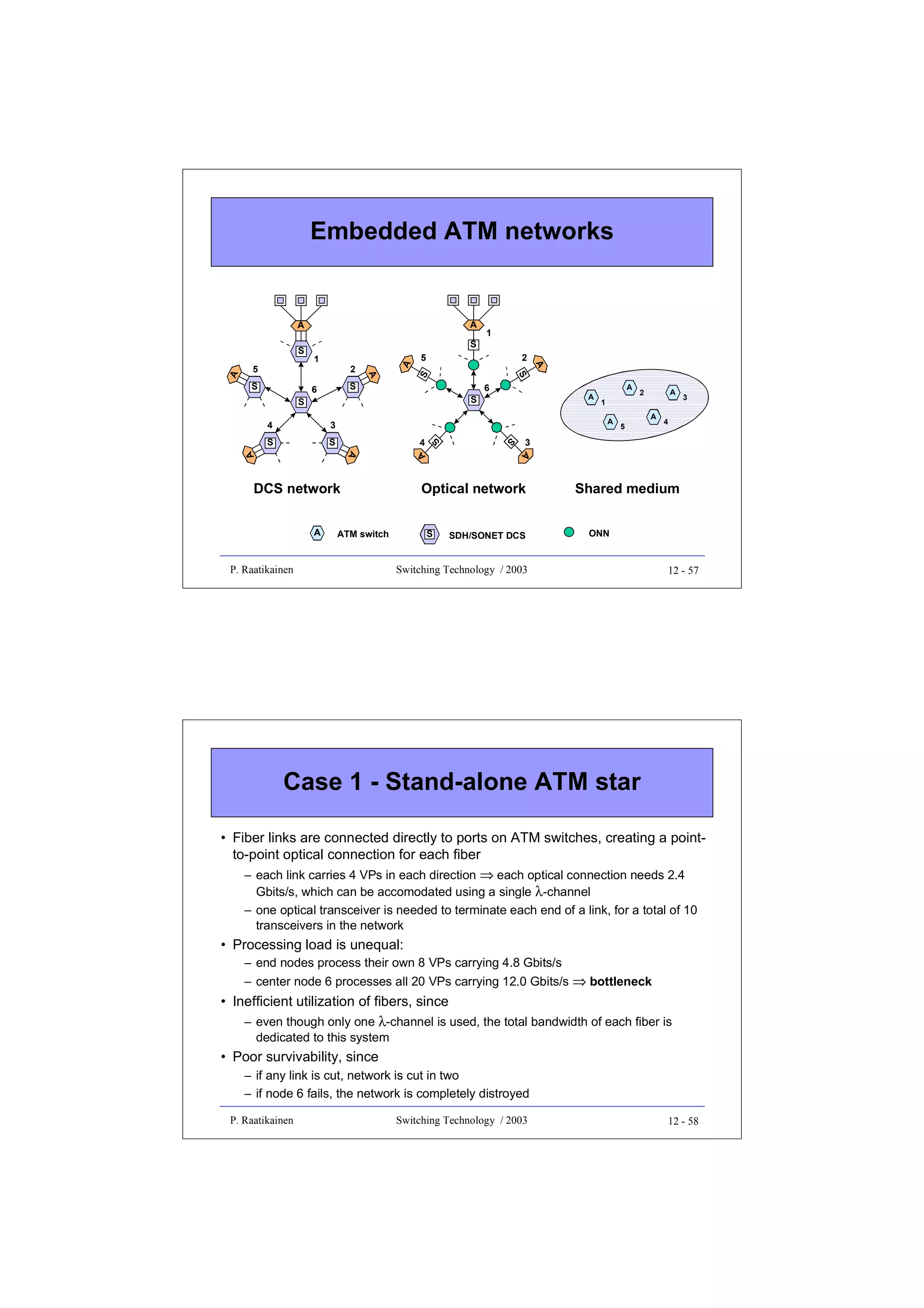
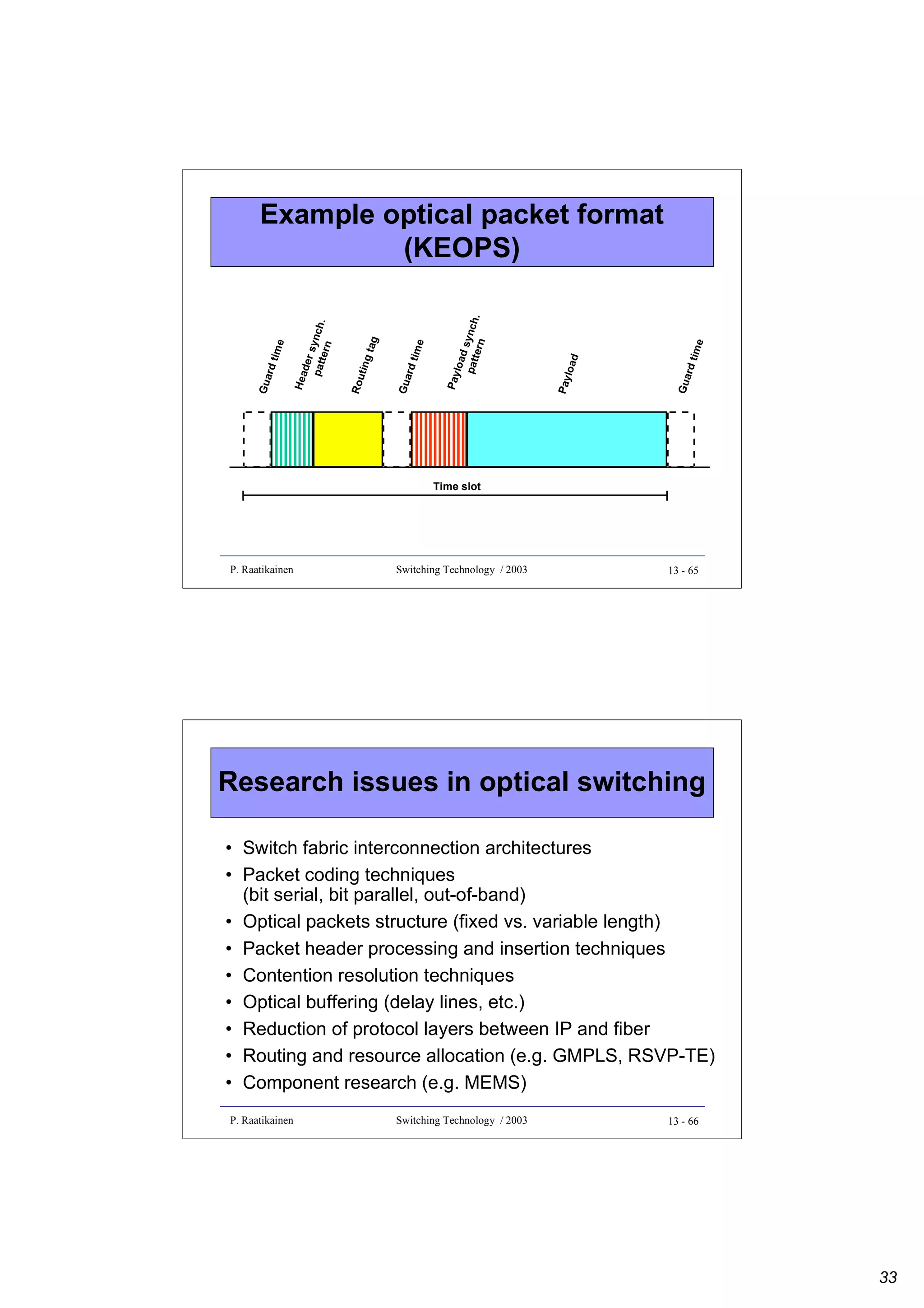
![GFP client data frame
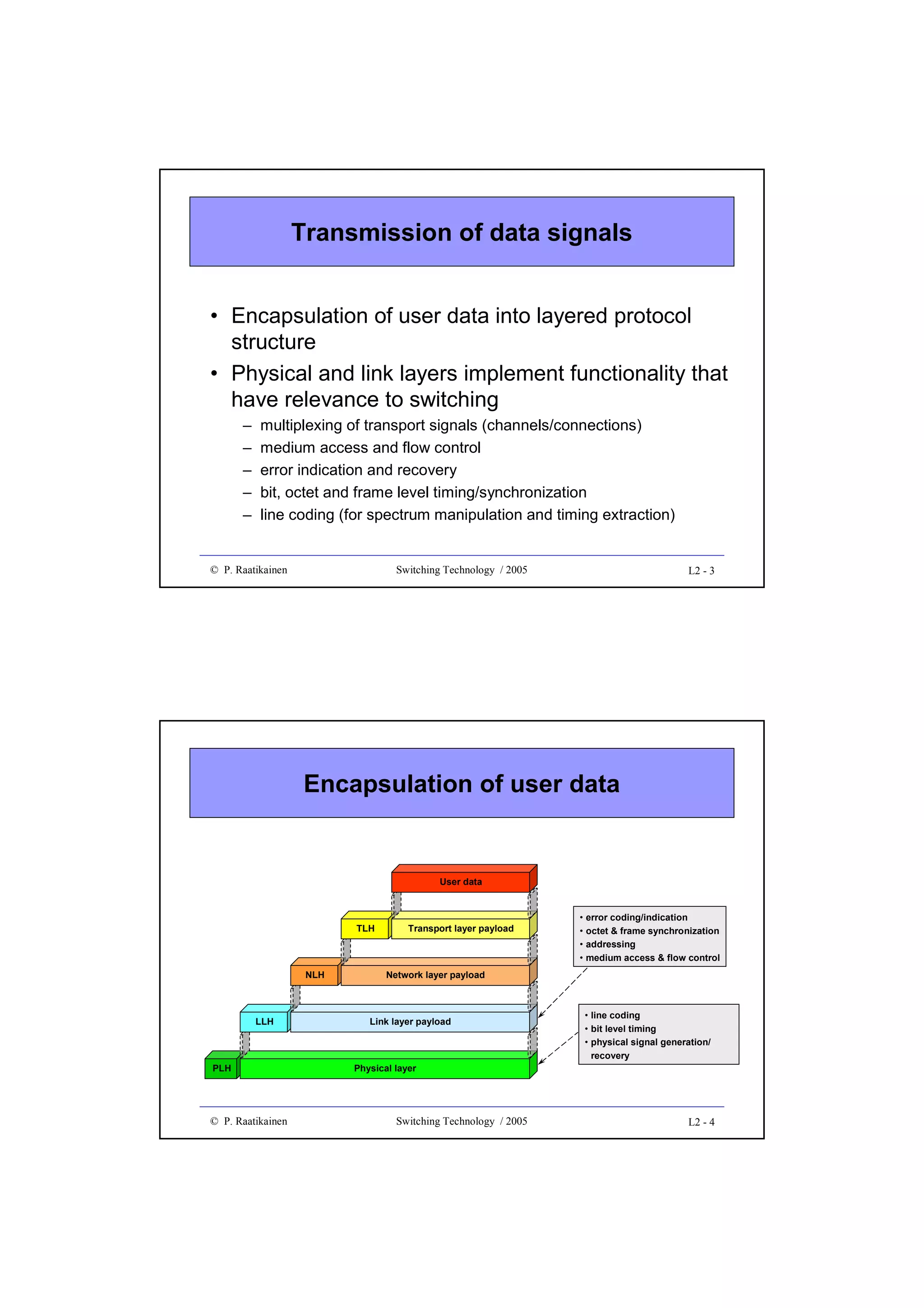
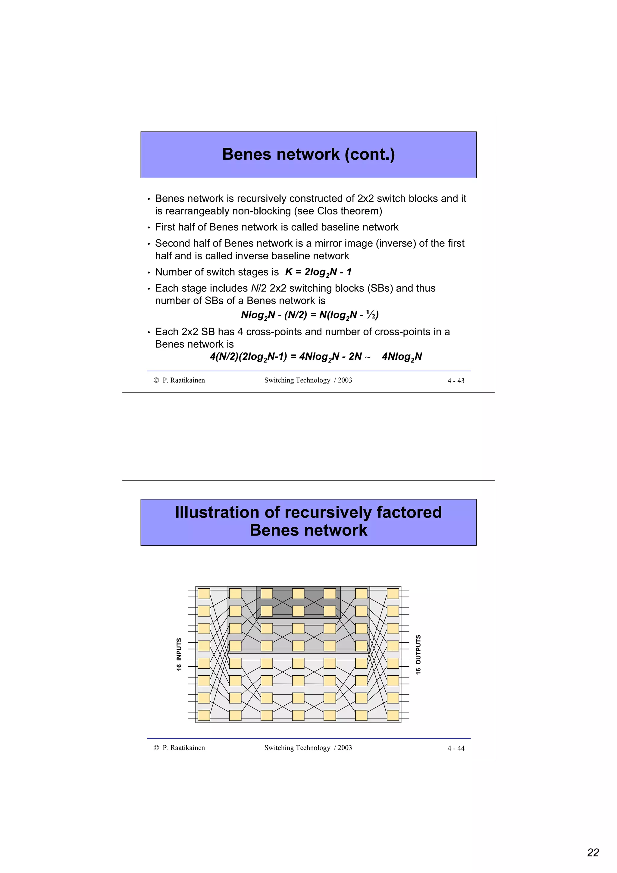
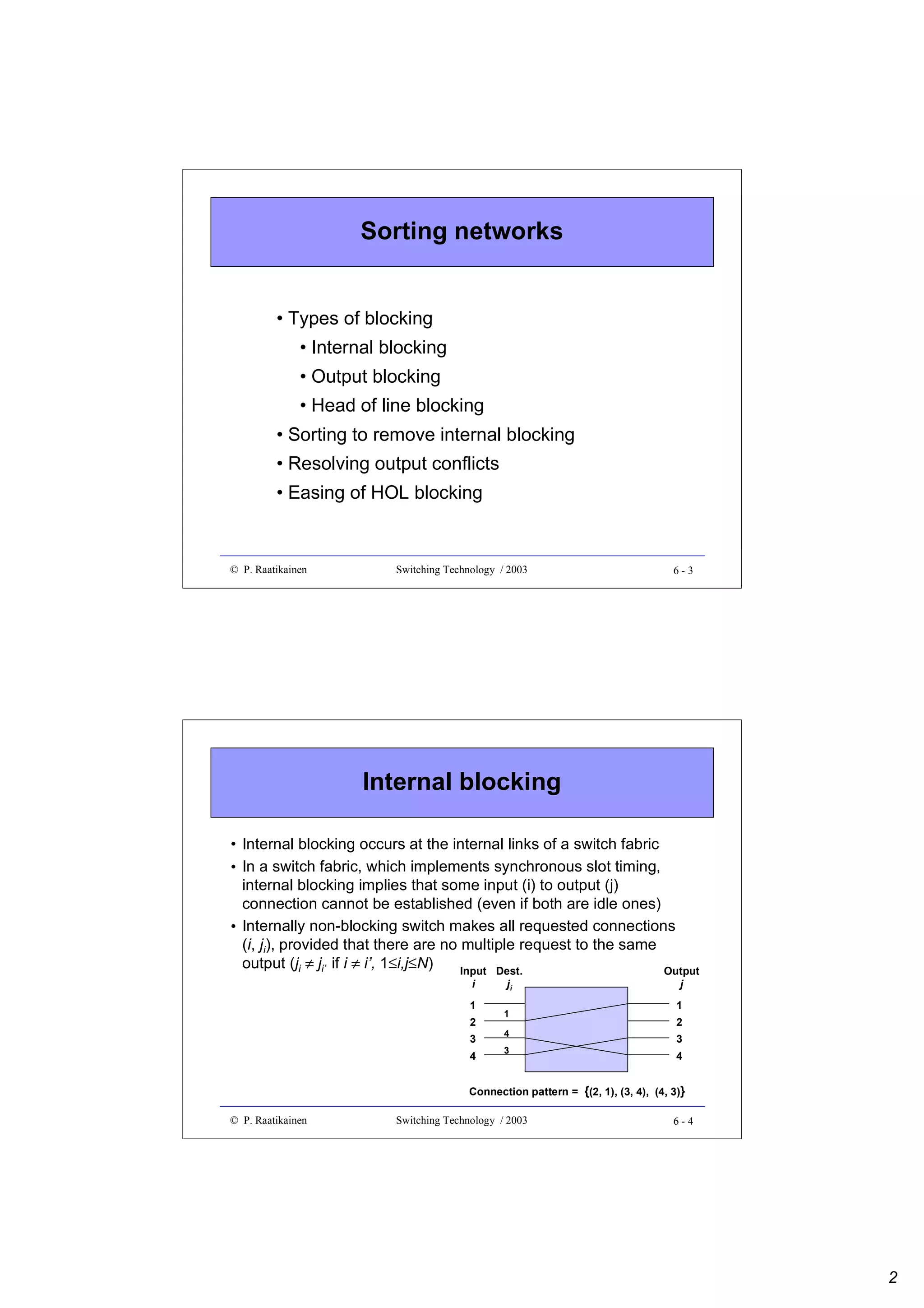
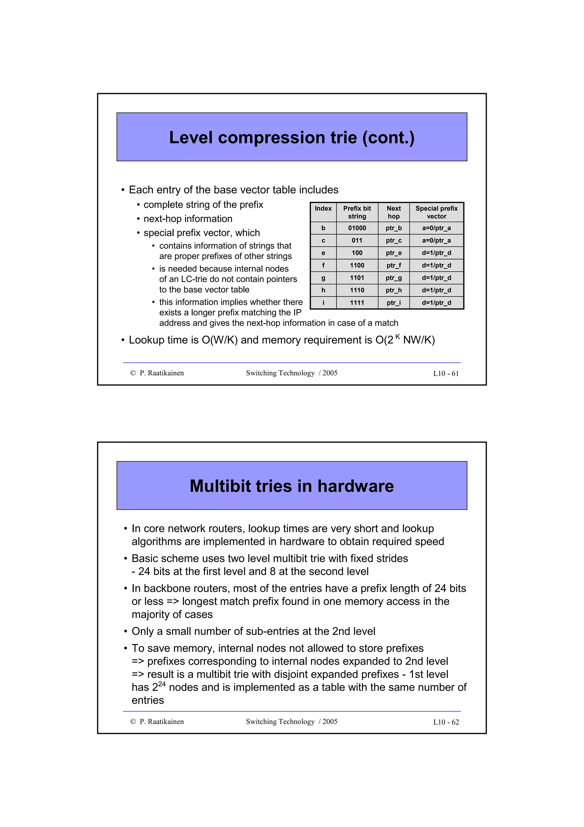
• Composed of a frame header and payload
• Core header intended for data link management
– payload length indicator (PLI, 2 octets), HEC (CRC-16, 2 octets)
• Payload field divided into payload header, payload and optional FCS
(CRC-32) sub-fields
• Payload header includes:
– payload type (2 octets) and type HEC (2 octets) sub-fields
– optional 0 - 60 octets of extension header
• Payload:
– variable length (0 - 65 535 octets, including payload header and FCS) for
frame mapping mode (GFP-F) - frame multiplexing
– fixed size Nx[536, 520] for transparent mapping mode (GFP-T) - no frame
multiplexing
© P. Raatikainen
Switching Technology / 2005
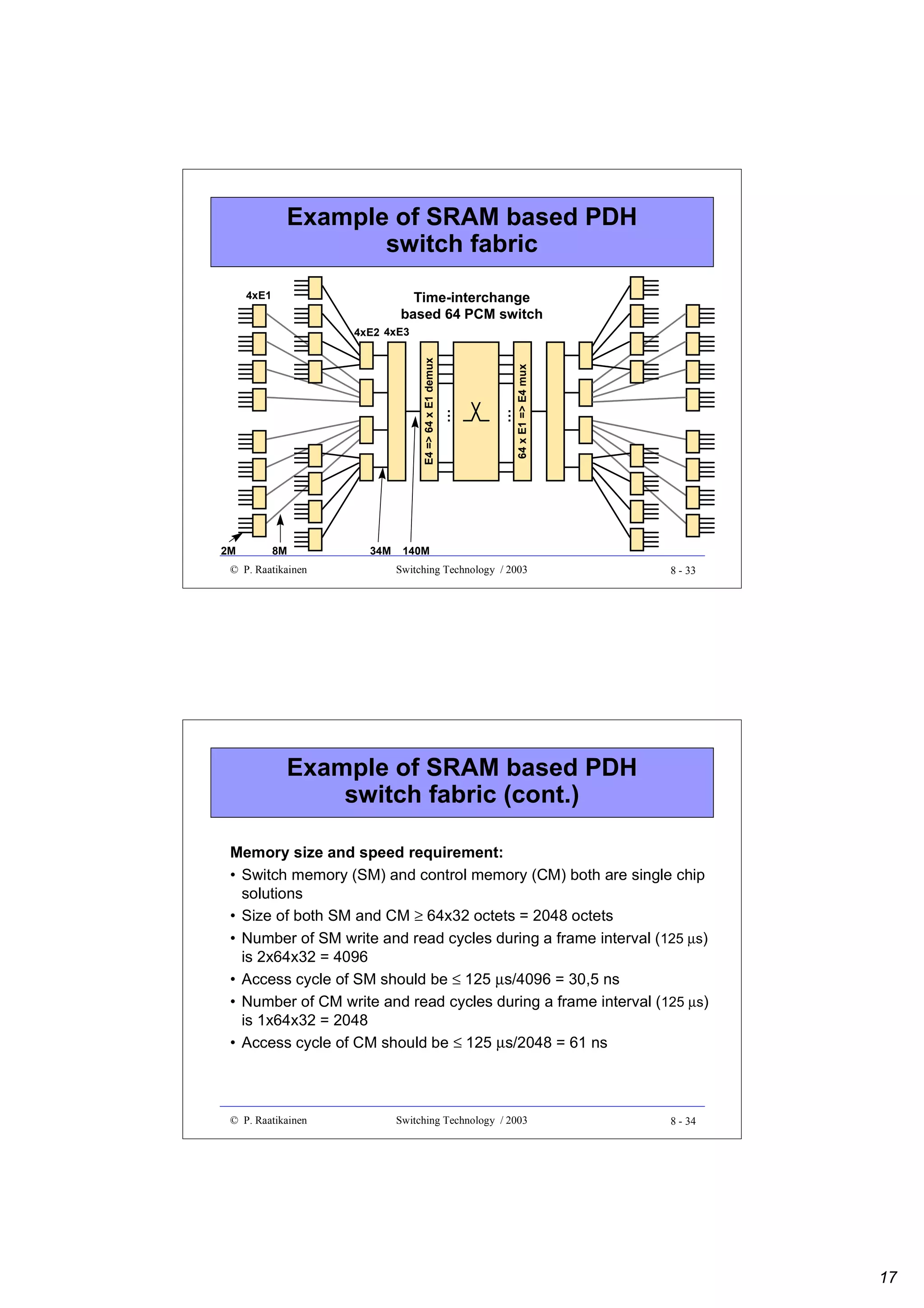
L2 - 61
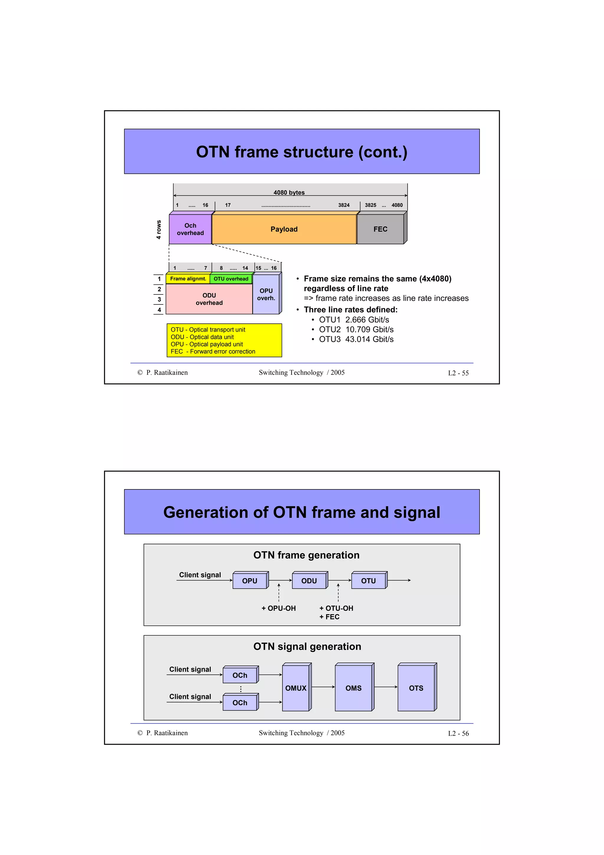
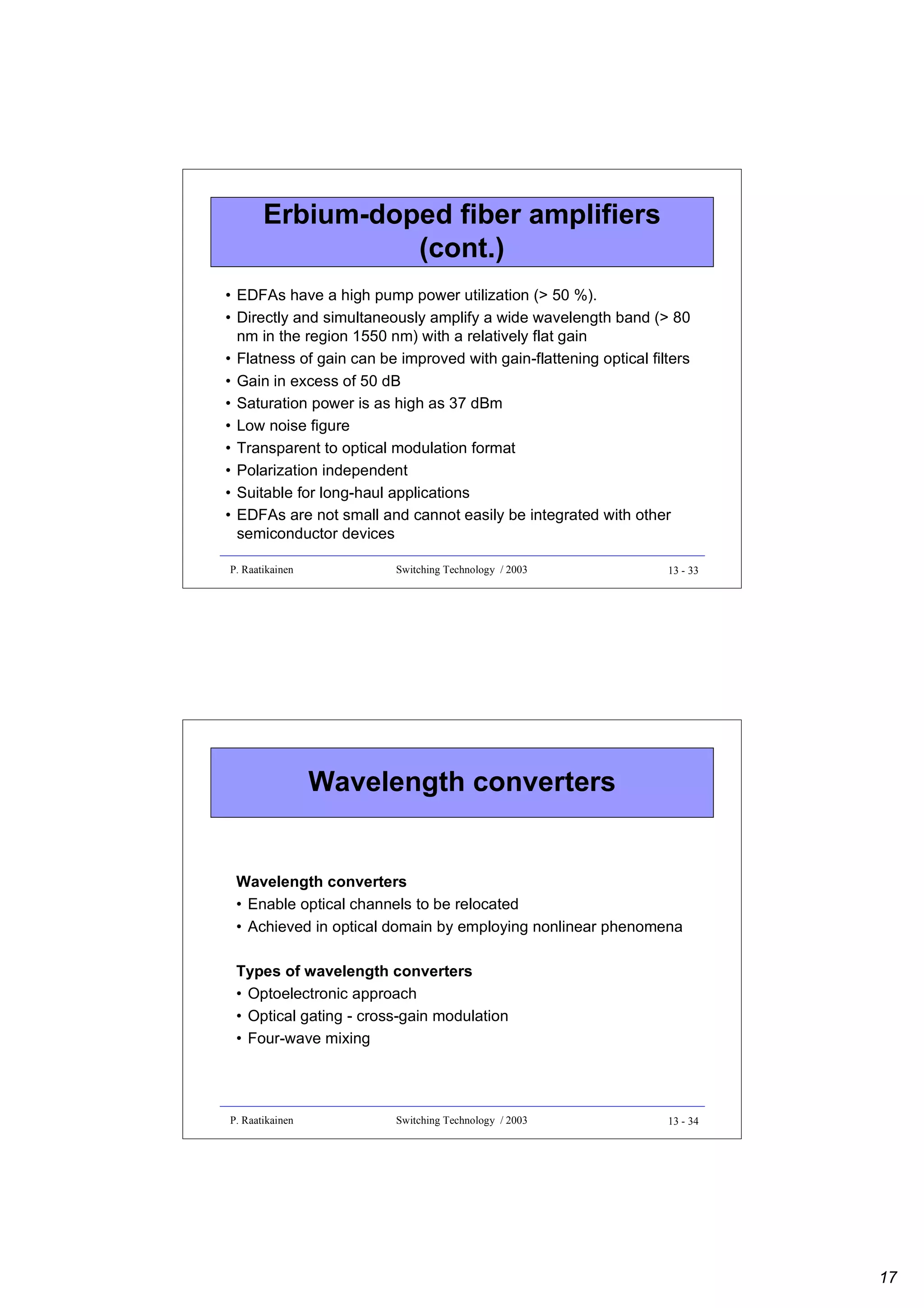
GFP frame structure
Payload length indicator
Core
header
Core HEC
PFI
EXI
UPI
Type HEC
CID
Payload header
Payload
area
PTI
Payload type
0 – 60 bytes
extension header
(optional)
Spare
Extension HEC MSB
Extension HEC LSB
Payload
[N x 536, 520 bytes
or variable length
packet]
Payload FCS
CID - Channel identifier
FCS - Frame Check Sequence
EXI - Extension Header Identifier
HEC - Header Error Check
PFI - Payload FCS Indicator
PTI - Payload Type Indicator
UPI - User payload Identifier
Source: IEEE Communications Magazine, May 2002
© P. Raatikainen
Switching Technology / 2005
L2 - 62](https://image.slidesharecdn.com/optix-core-good-140111131404-phpapp02/75/Optical-Switching-Comprehensive-Article-57-2048.jpg)
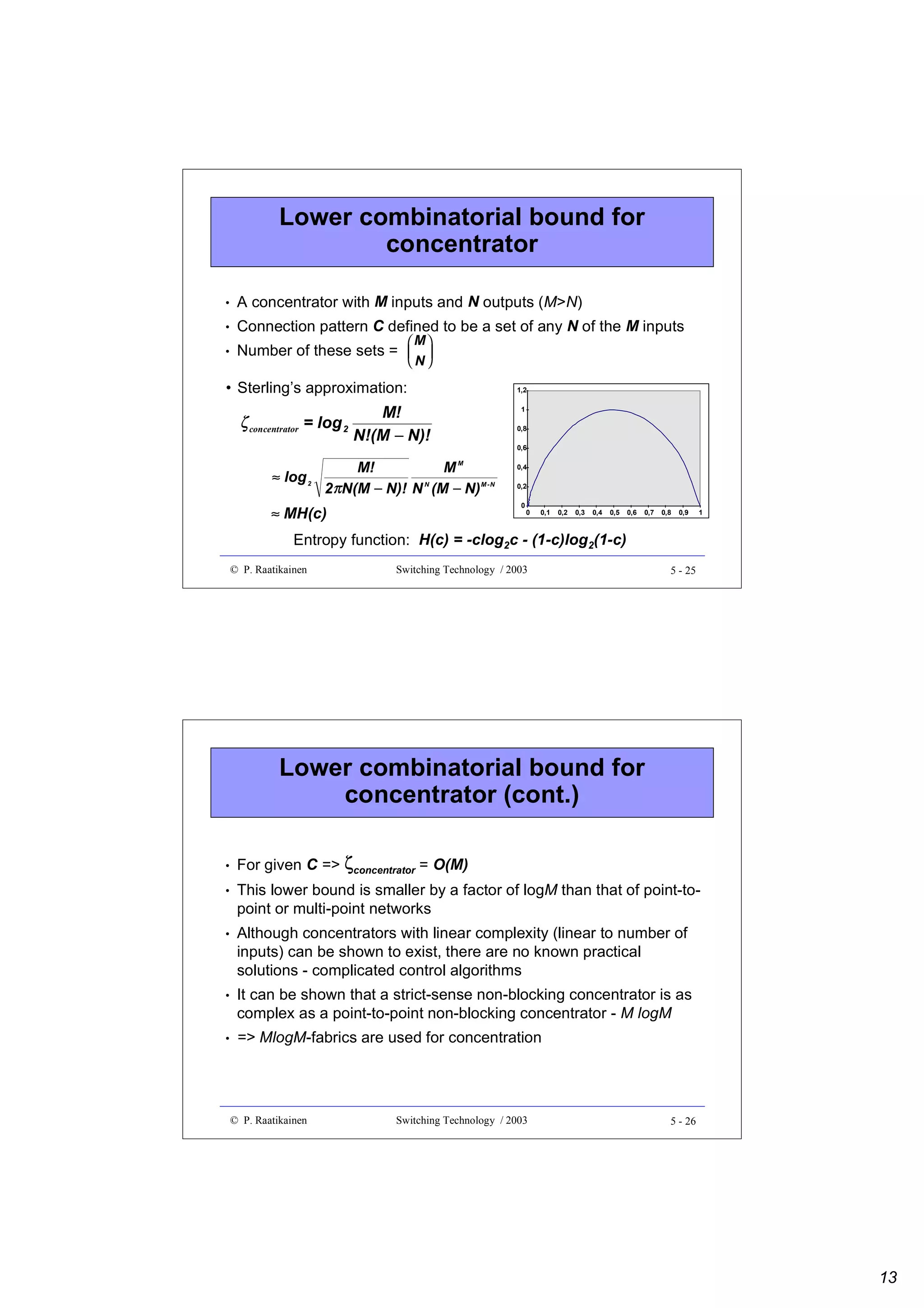
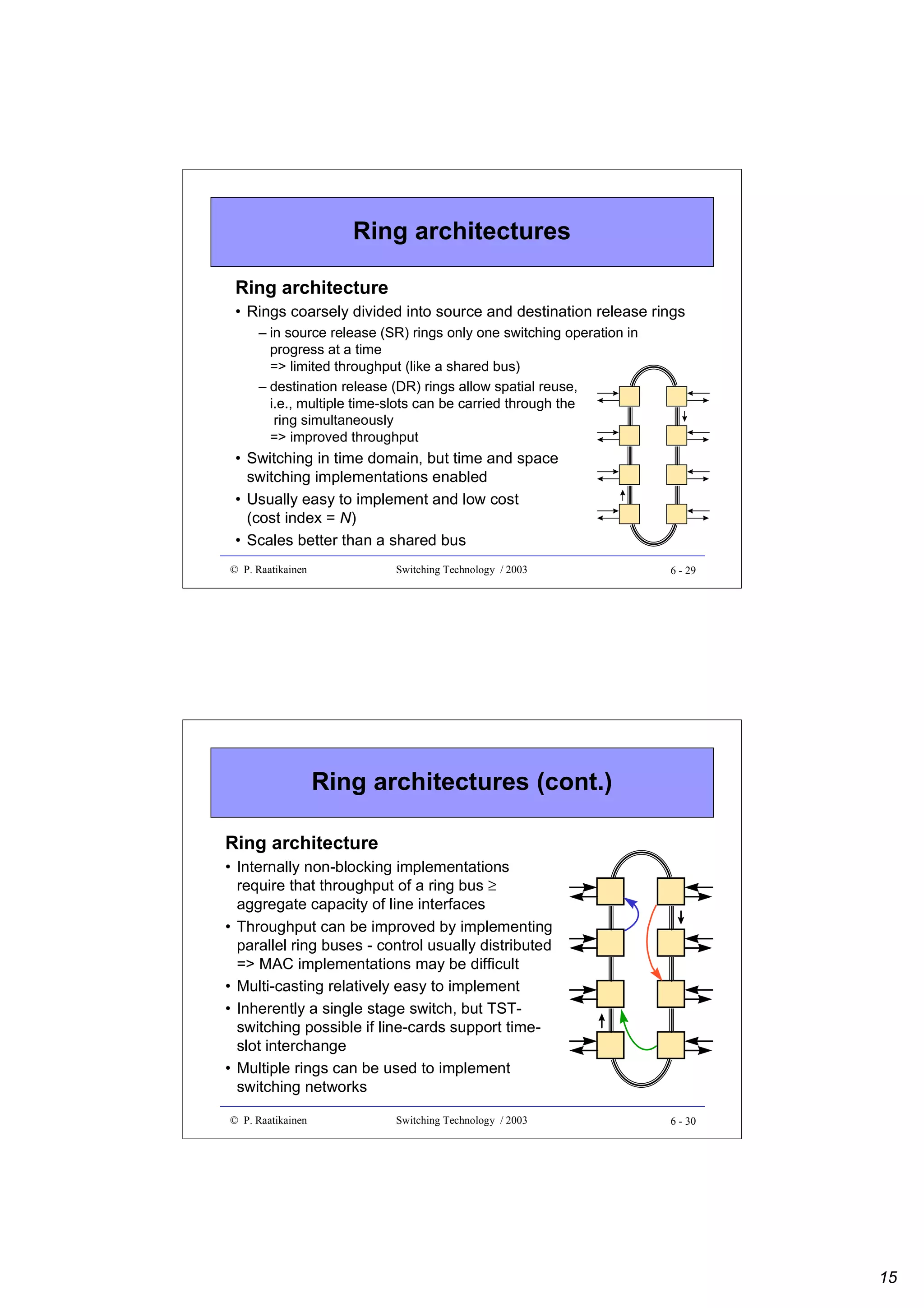
![Throughput
• Throughput gives forwarding/switching speed/efficiency of a
switch fabric
• It is measured in bits/s, octets/s, cells/s, packet/s, etc.
• Quite often throughput is given in the range (0 ... 1.0], i.e. the
obtained forwarding speed is normalized to the theoretical
maximum throughput
© P. Raatikainen
Switching Technology / 2003
3 - 11
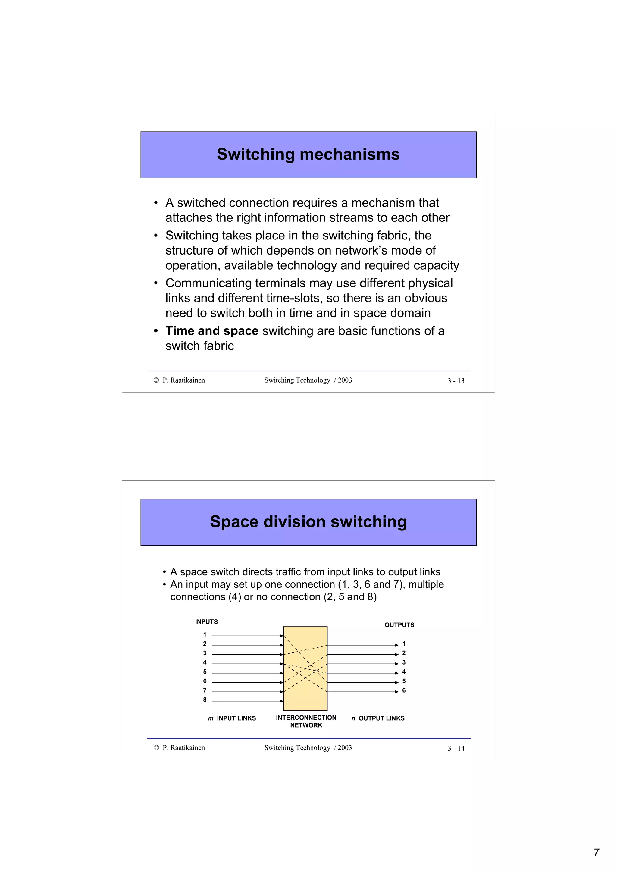
Switch fabrics
•
•
•
•
•
•
Basic concepts
Time and space switching
Two stage switches
Three stage switches
Cost criteria
Multi-stage switches and path search
© P. Raatikainen
Switching Technology / 2003
3 - 12
6](https://image.slidesharecdn.com/optix-core-good-140111131404-phpapp02/75/Optical-Switching-Comprehensive-Article-65-2048.jpg)
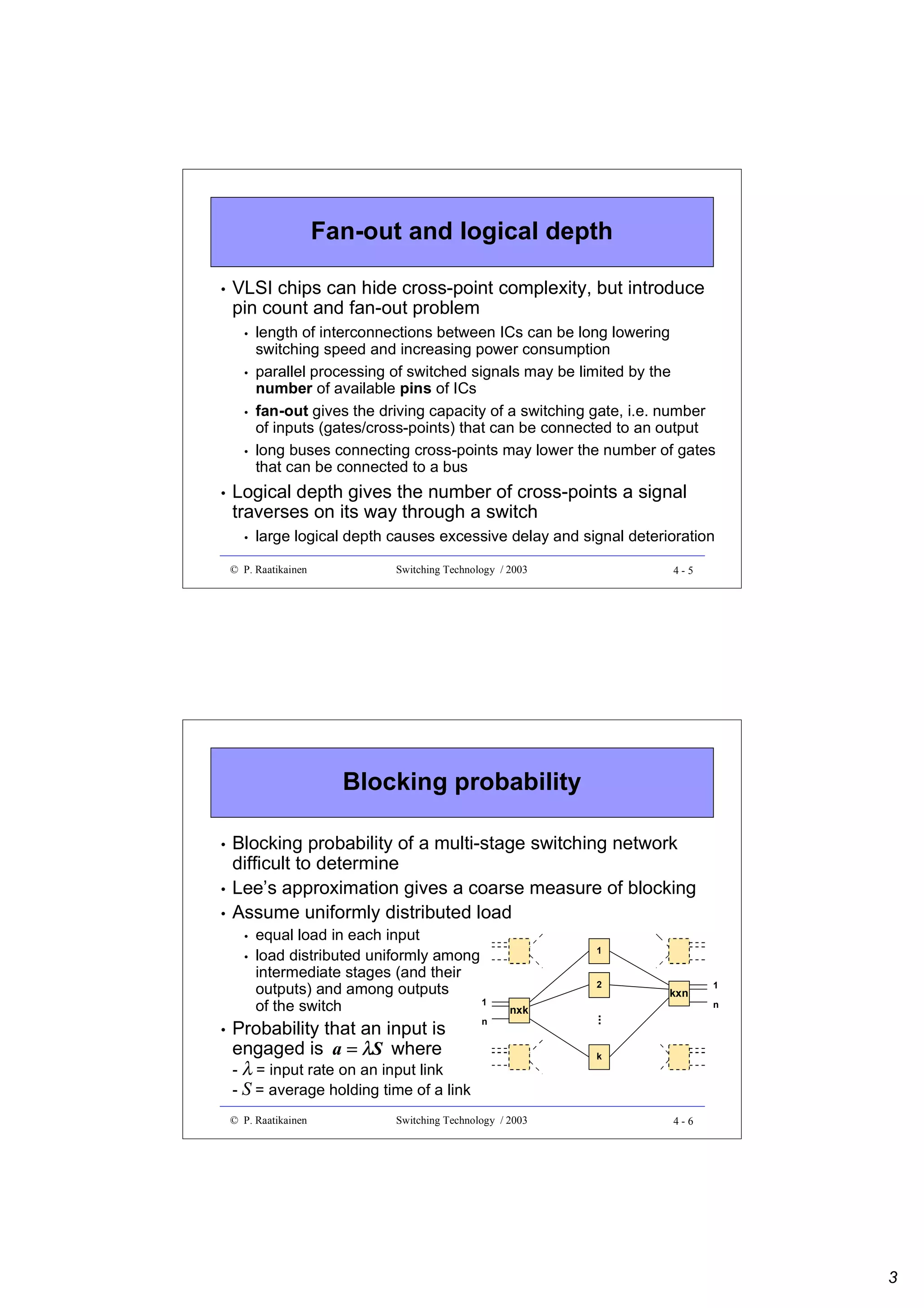
![Blocking probability (cont.)
•
•
•
Under the assumption of uniformly distributed load,
probability that a path between any two switching blocks
≥
is engaged is p = an/k (k≥n)
Probability that a certain path from an input block to an
output block is engaged is 1 - (1-p)2 where the last term is
the probability that both (input and output) links are
disengaged
Probability that all k paths between an input switching
block and an output switching block are engaged is
B = [1 - (1- an/k )2 ]k
which is known as Lee’s approximation
© P. Raatikainen
Switching Technology / 2003
4-7
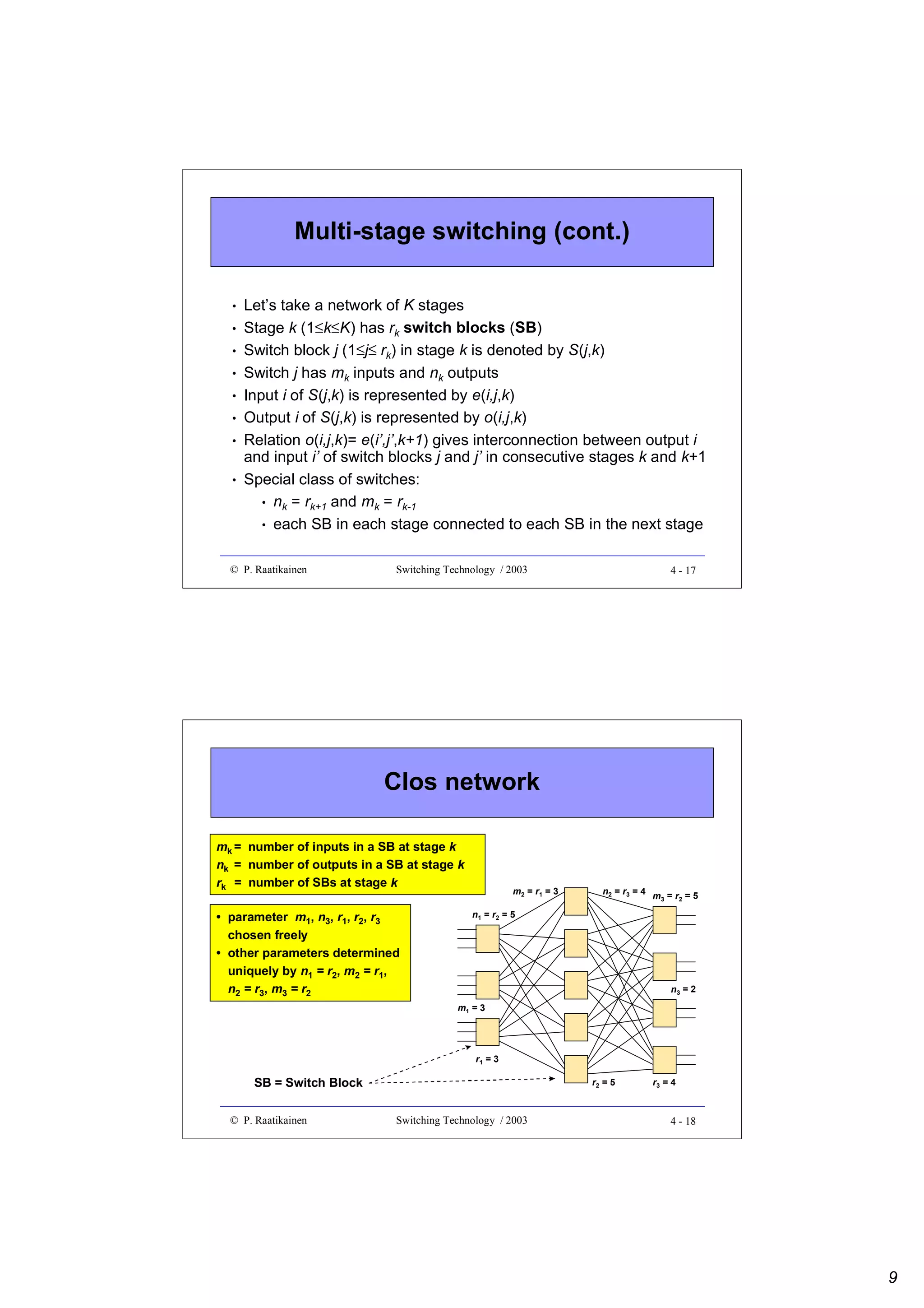
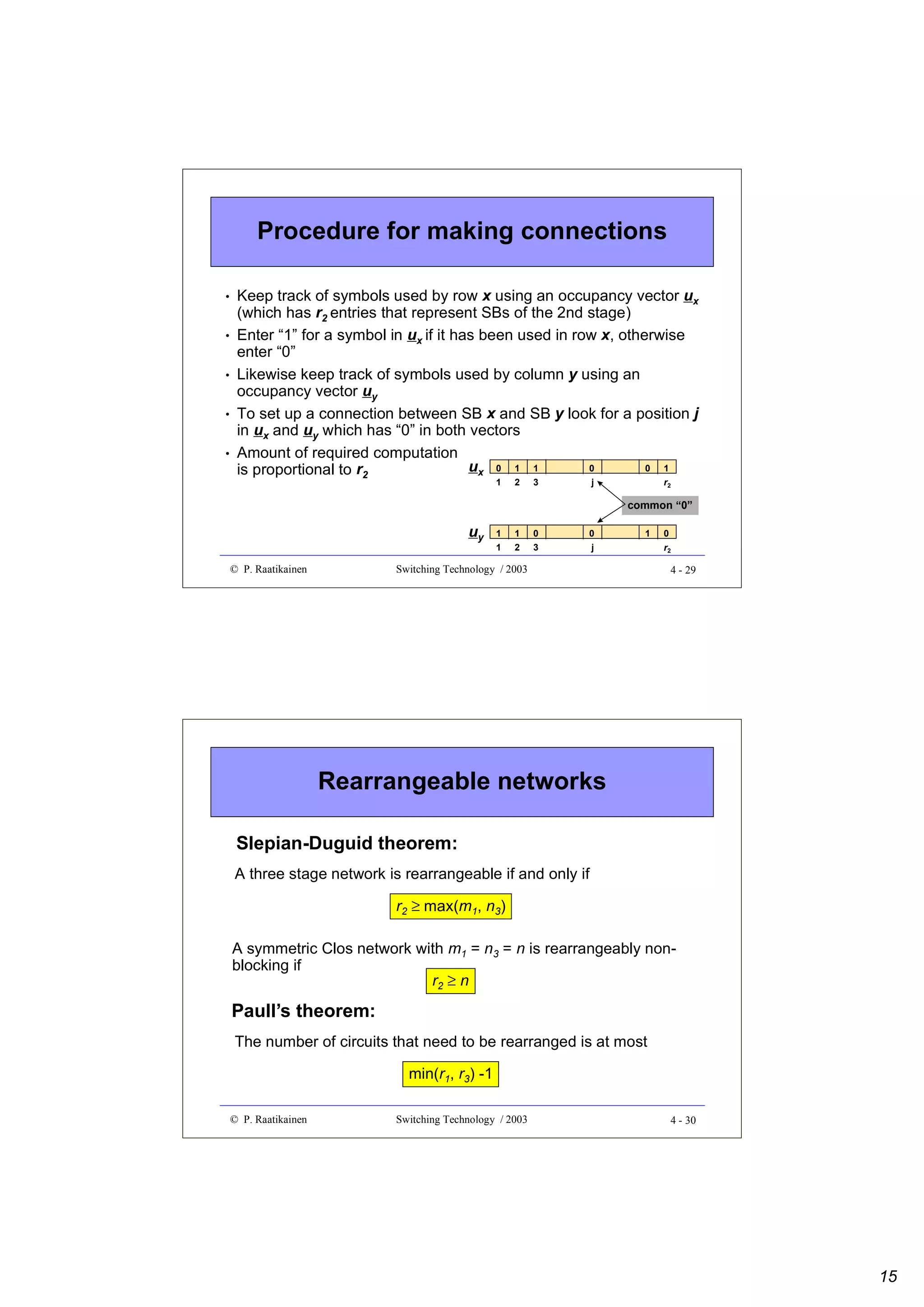
Control complexity
•
Give a graph G , a control algorithm is needed to find and set up
paths in G to fulfill connection requirements
•
Control complexity is defined by the hardware (computation and
memory) requirements and the run time of the algorithm
•
Amount of computation depends on blocking category and degree of
blocking tolerated
•
In general, computation complexity grows exponentially as a function
of the number of terminal
•
There are interconnection networks that have a regular structure for
which control complexity is substantially reduced
•
There are also structures that can be distributed over a large number
of control units
© P. Raatikainen
Switching Technology / 2003
4-8
4](https://image.slidesharecdn.com/optix-core-good-140111131404-phpapp02/75/Optical-Switching-Comprehensive-Article-85-2048.jpg)
![Management complexity
•
•
Network management involves adaptation and maintenance of a
switching network after the switching system has been put in place
Network management deals with
• failure events and growth in connectivity demand
• changes of traffic patterns from day to day
• overload situations
• diagnosis of hardware failures in switching system, control system
as well as in access and trunk network
- in case of failure, traffic is rerouted through redundant built-in
hardware or via other switching facilities
- diagnosis and failure maintenance constitute a significant part of
software of a switching system
•
In order for switching cost to grow linearly in respect to total traffic,
switching functions (such as control, maintenance, call processing and
interconnection network) should be as modular as possible
© P. Raatikainen
Switching Technology / 2003
4-9
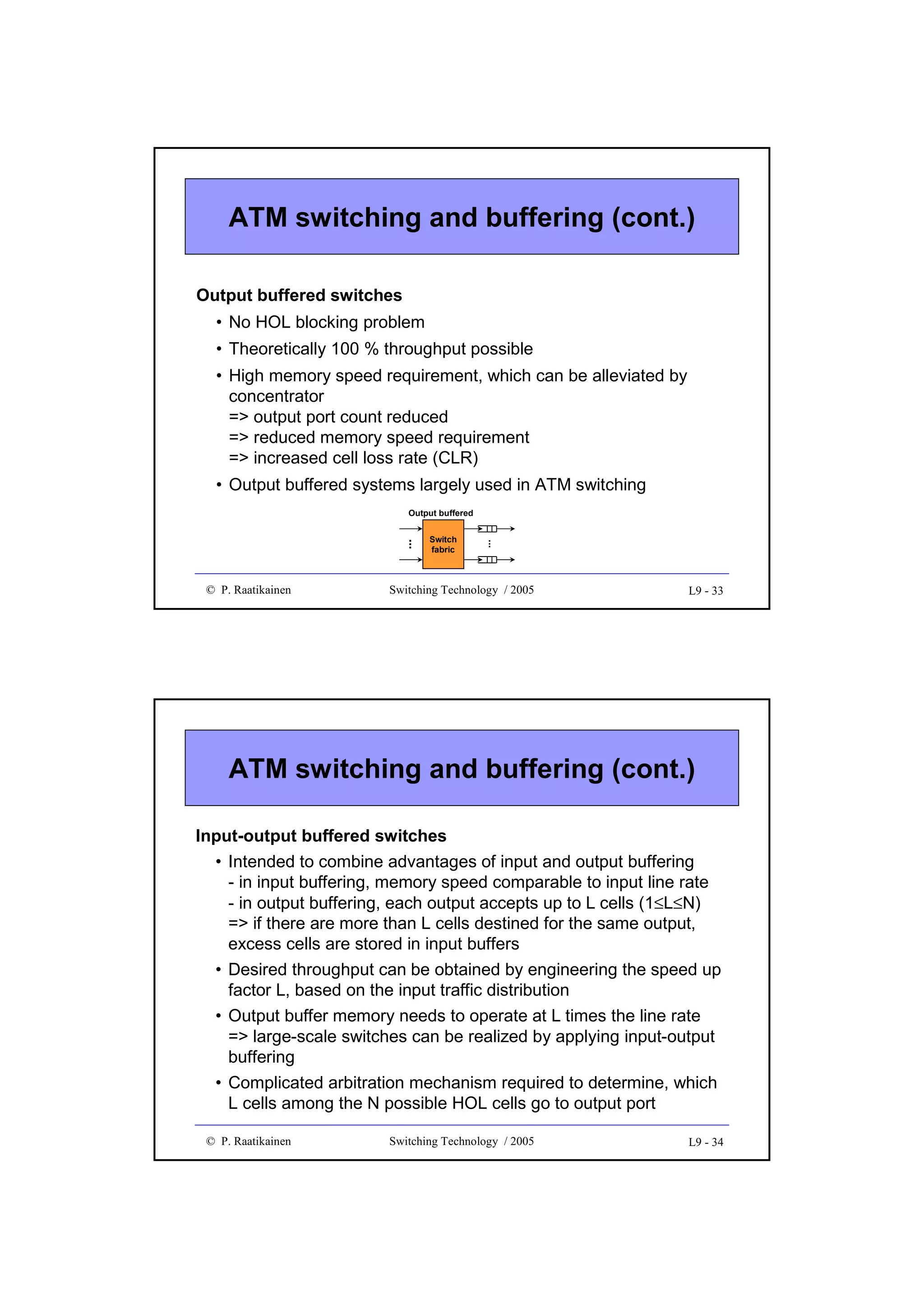
Example 1
•
A switch with
•
•
•
•
a capacity of N simultaneous calls
average occupancy on lines during busy hour is X Erlangs
Y % requirement for internal use
notice that two (one-way) connections are needed for a call
requires a switch fabric with M = 2 x [(100+Y)/100] x(N/X) inputs
and outputs.
•
If N = 20 000, X = 0.72 and Y = 10%
=> M = 2 x 1.1 x 20 000/0.72 = 61 112
=> corresponds to 2038 E1 links
1
2
2
M
© P. Raatikainen
Switching Technology / 2003
1
M
4 - 10
5](https://image.slidesharecdn.com/optix-core-good-140111131404-phpapp02/75/Optical-Switching-Comprehensive-Article-86-2048.jpg)
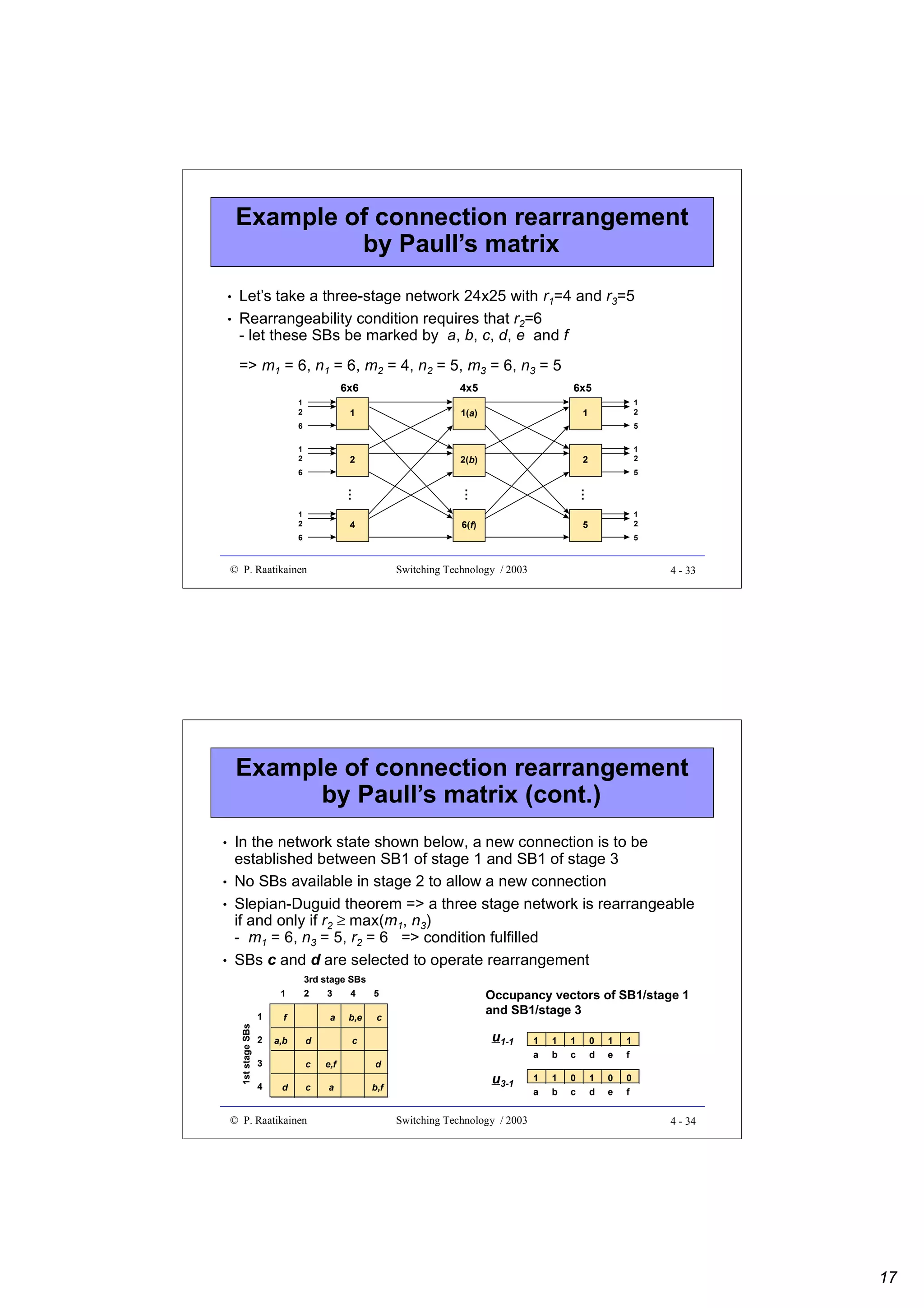
![Example 2
•
An exchange for 2000 subscribers is to be installed and it is
required that the blocking probability should be below 10 %.
If E2 links are used to carry the subscriber traffic to
telephone network, how many E2 links are needed ?
- average call lasts 6 min
- a subscriber places one call during a 2-hour busy period
(on the average)
• Amount of offered traffic is (2000x6 min /2x60 min) = 100 Erl.
• Erlang 1st formula gives for 10 % blocking and load of 100 Erl.
that n = 97
=> required number of E1 links is ceil(97/30) = 4
© P. Raatikainen
Switching Technology / 2003
4 - 13
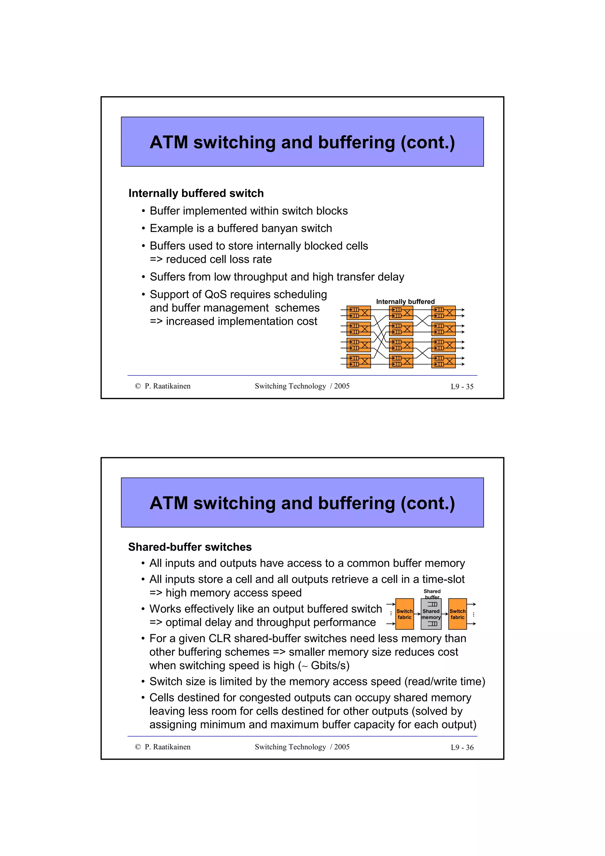
Example 3
•
•
•
Suppose driving current of a switching gate (cross-point) is 100 mA
and its maximum input current is 8 mA
How many output gates can be connected to a bus, driven by one
input gate, if the capacitive load of the bus is negligibly small ?
Fan-out = floor[100/8] = 12
c
c
• How many output gates can be connected
to a bus driven by one input gate if load of
the bus corresponds to 15 % of the load of
a gate input) ?
• Fan-out = floor[100/(1.15x8)] = 10
© P. Raatikainen
Switching Technology / 2003
c
1
c
2
…
M
4 - 14
7](https://image.slidesharecdn.com/optix-core-good-140111131404-phpapp02/75/Optical-Switching-Comprehensive-Article-88-2048.jpg)
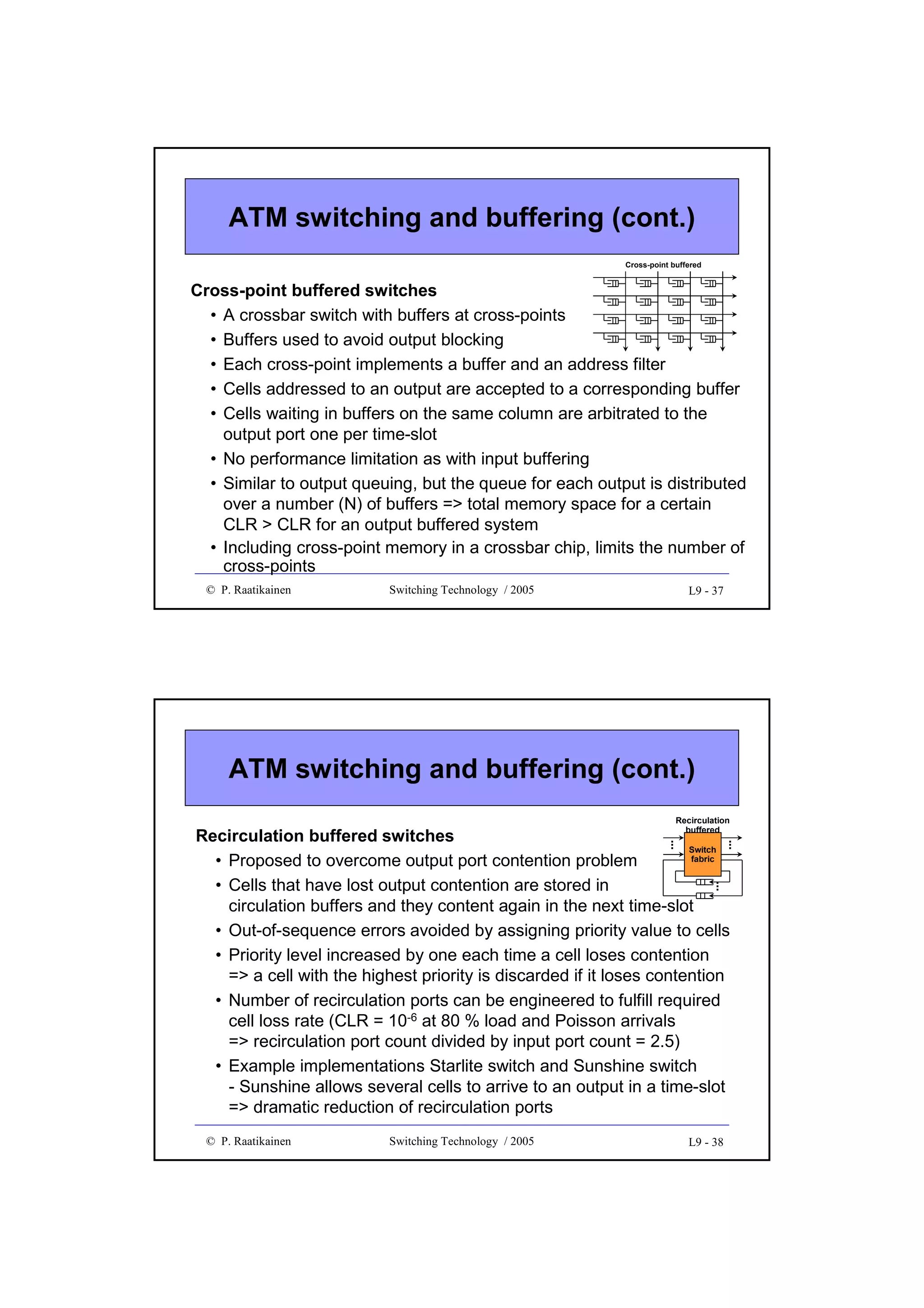
![Cantor network strict-sense
non-blocking (cont.)
•
Cantor network is symmetrical at the middle
=> the same number of center stage nodes are reachable by an
output of a Cantor network
•
Total number of SBs in center stages is Nm/2 (m Benes networks)
•
If the number of center stage SBs reached by an input and an
output exceeds Nm/2 then there must be a SB reachable from both
•
Hence strict-sense non-blocking is achieved if
2 [1 Nm - 1 (log 2 N - 1)N ] >
2
4
Nm
2
=> m > log2N - 1
Notice that a strict-sense non-blocking Cantor network is
constructed of log2N rearrangeably non-blocking Benes networks
© P. Raatikainen
Switching Technology / 2003
5-7
N INPUTS
N OUTPUTS
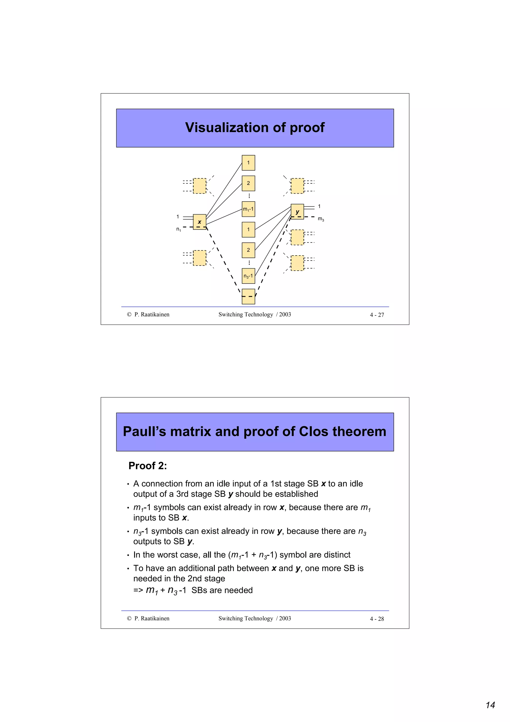
Visualization of proof
© P. Raatikainen
Switching Technology / 2003
5-8
4](https://image.slidesharecdn.com/optix-core-good-140111131404-phpapp02/75/Optical-Switching-Comprehensive-Article-107-2048.jpg)

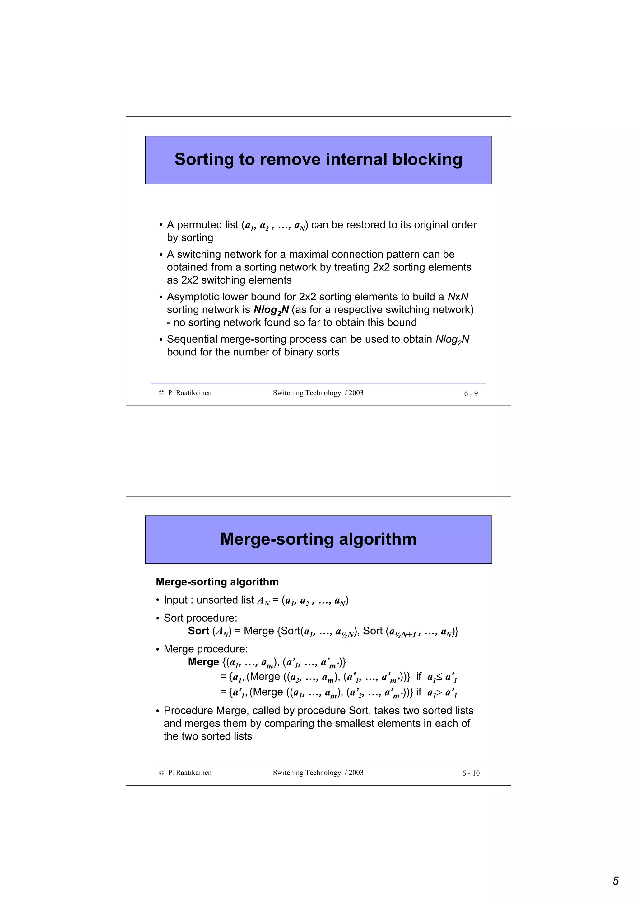
![Merge-sorting algorithm (cont.)
• Merging of two sorted lists (N/2 numbers in each) requires N
binary sorts
• Total complexity of sorting N numbers is given by
C(N) = 2C(N/2) = N + 2(N/2 + 2C(N/4)) = … = Nlog2N
• Due to sequential nature of procedure Merge the sorting takes at
least O(N) time
1
4
6
10
11
15
17
20
© P. Raatikainen
Compare numbers
at the top of lists
then merge
2
5
7
9
12
14
16
24
Switching Technology / 2003
6 - 11
Odd-even merging
Recursive construction of an odd-even merger
...
¥ ¥
...
...
...
e0
e1
e2
e3
e4
eN/2-5
eN/2-4
eN/2-3
eN/2-2
eN/2-1
cN/2-2
cN/2-1
Odd
merger
N/2 dN/2-3
...
bN/2-4
bN/2-3
bN/2-2
bN/2-1
...
...
...
d0
d1
...
b0
b1
© P. Raatikainen
¥ ¥
...
aN/2-2
aN/2-1
Even
merger
N/2
c0
c1
c2
...
a0
a1
a2
a3
...
- number of sorting stages is log2N
- number of sorting elements is 0.5N [log2N-1]+1
dN/2-2
dN/2-1
Switching Technology / 2003
6 - 12
6](https://image.slidesharecdn.com/optix-core-good-140111131404-phpapp02/75/Optical-Switching-Comprehensive-Article-134-2048.jpg)
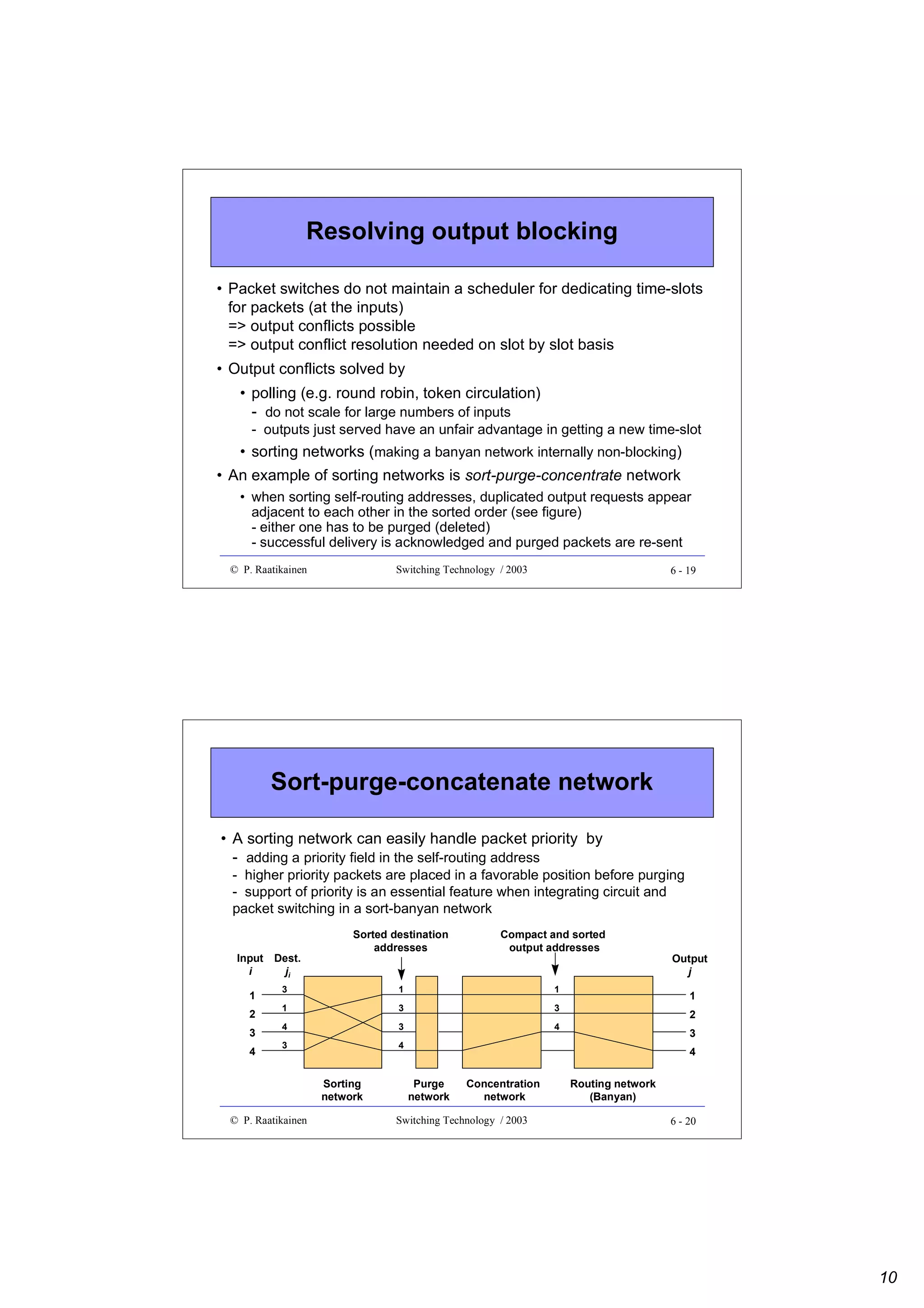
![Sorting by merging
Recursive construction of a sorting by merging network
- number of sorting stages is 0.5Nlog2N(log2N + 1)
¥
¥
Merger
N/2
¥
¥
¥
© P. Raatikainen
Merger
N
...
Merger
N/4
...
Merger
N/2
¥
Merger
N/4
...
...
aN-2
aN-1
Merger
N/4
¥
aN/2
aN/2+1
e0
¥
aN/2-1
...
...
...
aN/2-2
Merger
N/4
¥
a1
¥
a0
eN-1
Switching Technology / 2003
6 - 15
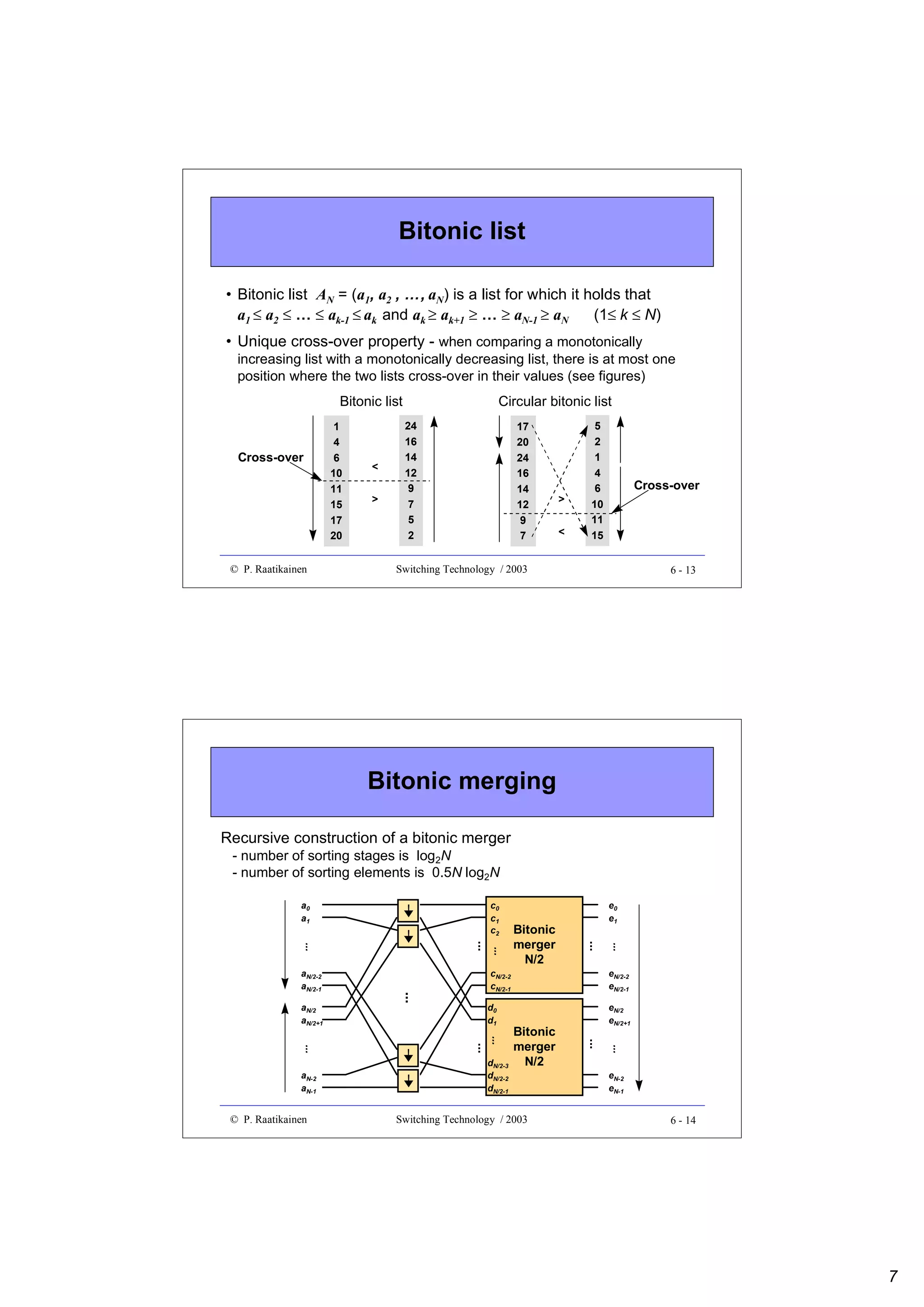
Odd-even sorting network example
• Number of sorting stages is 0.5log2N(log2N + 1)
• Number of sorting elements is 0.25N[log2N(log2N - 1) + 4] - 1
2x2
SORTER
4x4
SORTER
8x8
SORTER
¥ ¥
¥
¥ ¥
¥
¥
¥
¥ ¥
¥
¥ ¥
¥ ¥
¥
¥
¥
¥
¥ ¥
© P. Raatikainen
2x2 UP SORTER
2x2 DOWN SORTER
Switching Technology / 2003
6 - 16
8](https://image.slidesharecdn.com/optix-core-good-140111131404-phpapp02/75/Optical-Switching-Comprehensive-Article-136-2048.jpg)
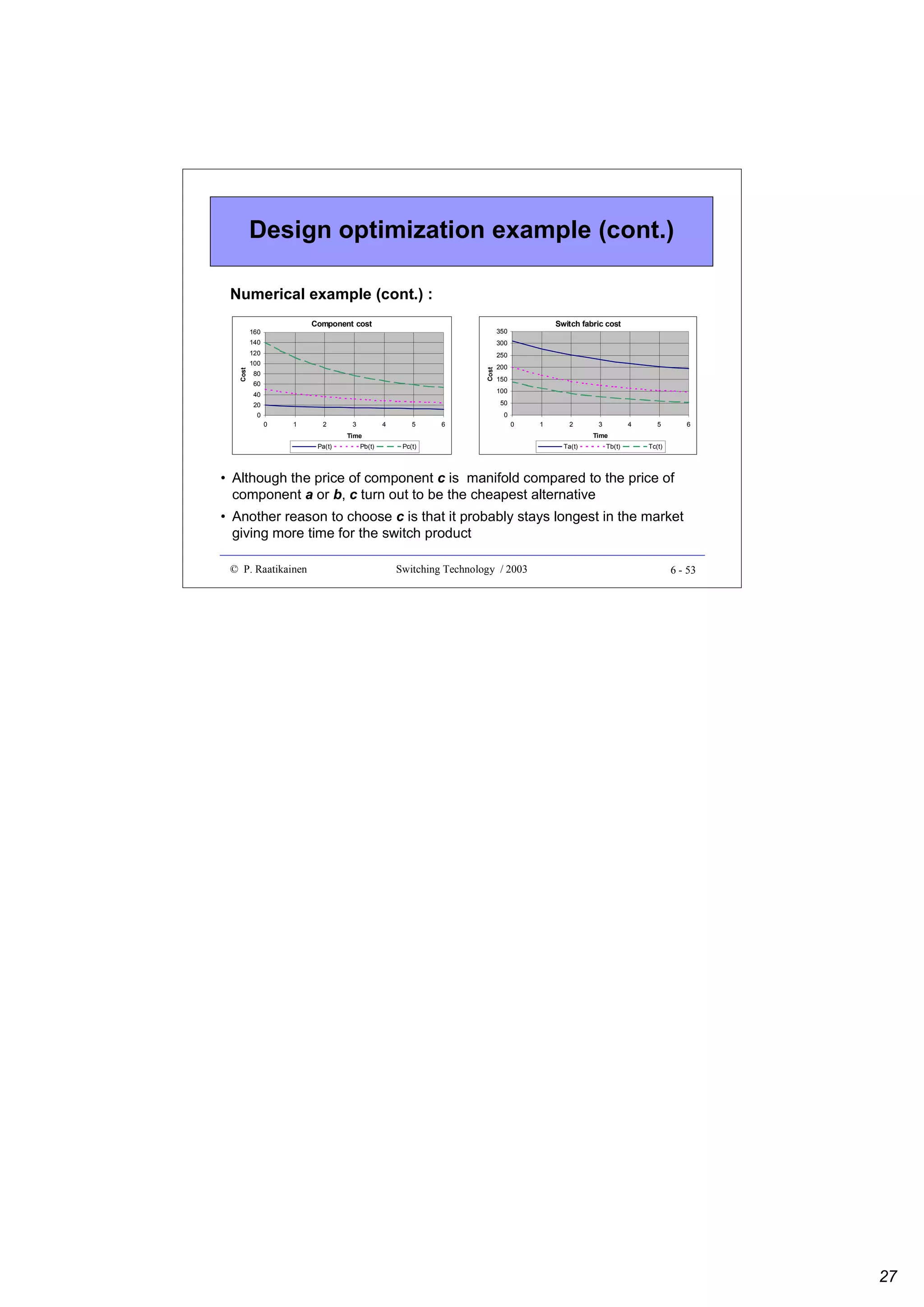
![Design optimization example (cont.)
• As an example, let’s assume that price of each component is a function of
time and is given by P(t)=Ce-t/T+ D ,
where C, D and T are component specific constants
=> Pa(t)=Cae-t/Ta+ Da , Pb(t)=Cbe-t/Tb+ Db and Pc(t)=Cce-t/Tc+ Dc
• Number of alternative crossbar components needed to build an NxN switch
=> Ka = ceil[N/Na]2, Kb = ceil[N/Nb]2 , Kc = ceil[N/Nc]2
• Alternative component costs as a function of time t
=> Pa(t)=Cae-(t- ta)/Ta+ Ca
=> Pb(t)=Cbe-(t- tb)/Tb+ Cb
=> Pc(t)=Cce-(t- tc)/Tc+ Cc
• These functions can be used to draw price development curves to make
comparisons
© P. Raatikainen
Switching Technology / 2003
6 - 51
Design optimization example (cont.)
Numerical example:
• Let N = 64, Na = 16, Nb = 32, Nc = 64, Ta = Tb = Tc = 3 time units (years),
Ca = 20,Cb = 50, Cc = 100 and Da = 10, Db = 20, Dc = 40 price units (euros)
• Product development period is assumed to be 1 time unit (year) and
tb = ta +1.5, tc = ta +3, tm = ta +4 => tpd = ta + 3
• Choosing that tpd = to = 0 => ta = t + 3, tb = t +1.5, tc = t, tm = t -1 (t ≥ tpd = 0 )
• Number of components needed Ka = 16, Kb = 4, Kc = 1
• Switch fabric component cost functions
=> Pa(t)=16[20e-(t+3)/3 + 10]
=> Pb(t)=4[50e-(t+1.5)/3 + 20]
=> Pc(t)=100e-(t)/3 + 40
© P. Raatikainen
Switching Technology / 2003
6 - 52
26](https://image.slidesharecdn.com/optix-core-good-140111131404-phpapp02/75/Optical-Switching-Comprehensive-Article-154-2048.jpg)
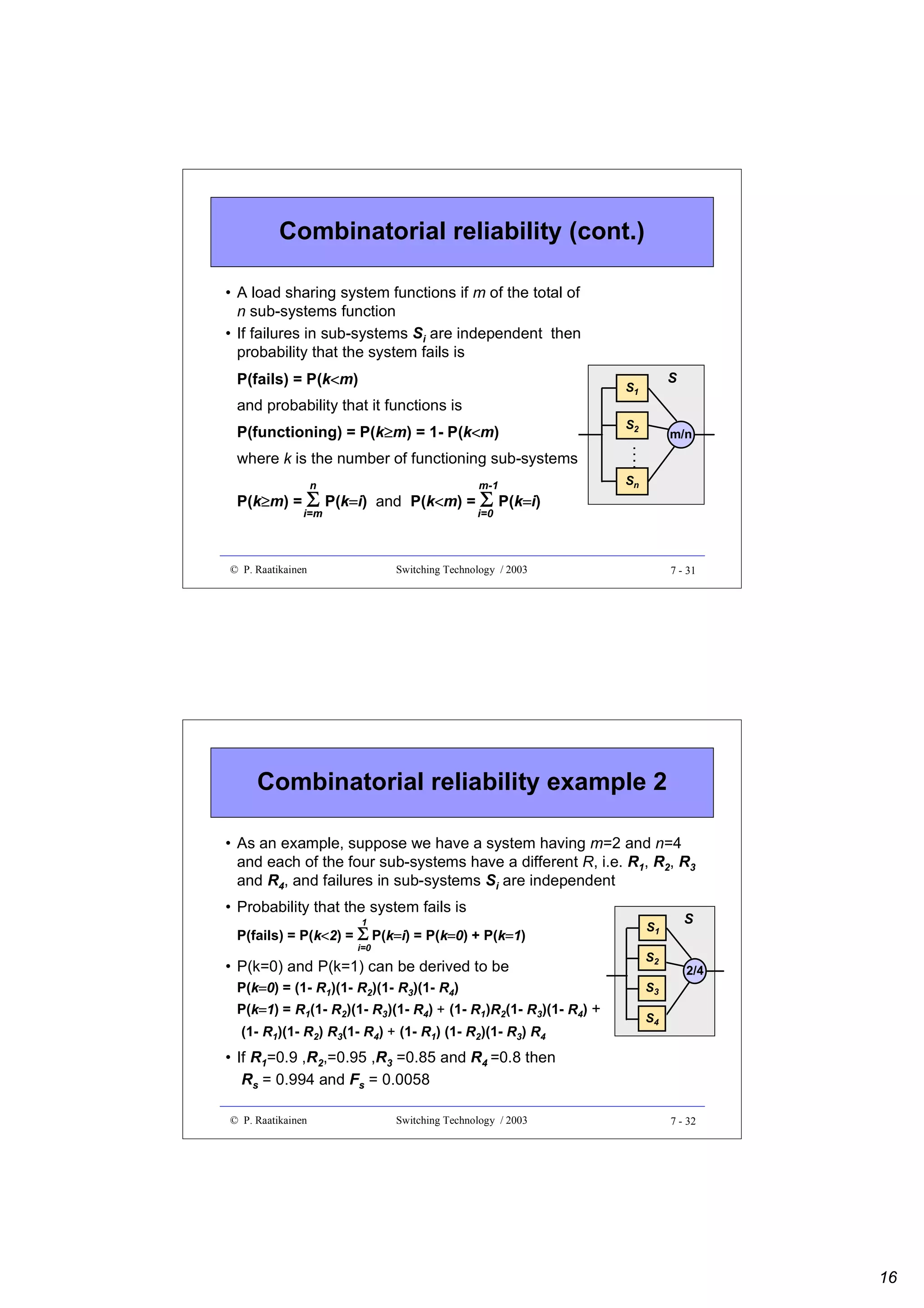
![Combinatorial reliability
• A serial system S functions if and only if all
its parts Si (1≤i≤n) function
S
n
=> Rs = Π Ri and Fs = (1- Rs)
S1
i=1
S2
Sn
• Failures in sub-systems are supposed to be
independent
S1
• A parallel (replicated) system fails if all its subsystems fail
n
=> Fs = Π (1-Ri)
i=1
S2
n
and Rs = 1- Fs = 1- Π (1-Ri)
i=1
Sn
• Reliability of a duplicated system (Ri = R) is
Rs = 1- (1-R)2
© P. Raatikainen
S
Switching Technology / 2003
7 - 29
Combinatorial reliability example 1
• Calculate reliability Rs and failure probability Fs of system S
given that failures in sub-systems Si are independent and for
some time interval it holds that
R1 = 0.90, R2 = 0.95 and R3 = R4 = 0.80
=> Rs = Π Ri = R1 x R2 x R3-4
=> R3-4 = 1- Π (1-Ri) = 1- (1- R3)(1- R4)
=> Rs = R1 x R2 x [1- (1- R3)(1- R4)]
S
S1
S3-4
S3
S2
S4
=> Fs = 1- Rs = 1 - R1 x R2 x [1- (1- R3)(1- R4)]
=> Rs = 0.82 and Fs = 0.18
© P. Raatikainen
Switching Technology / 2003
7 - 30
15](https://image.slidesharecdn.com/optix-core-good-140111131404-phpapp02/75/Optical-Switching-Comprehensive-Article-170-2048.jpg)
![Combinatorial reliability (cont.)
• If failures in sub-systems Si of an m/n system
are independent and Ri = R for all i∈[1,n]
then the system is a Bernoulli system and
binomial distribution applies
n
=> Rs =
Σ ( k )Rk(1-R)n-k
k=m
n
• For a system of m/n = 2/3
3
3!
−−−−
=> R2/3 = Σ k!(3-k)! Rk(1-R)3-k = 3R2 - 2R3
k=2
If for example R
S1
S2
S
m/n
Sn
= 0.9 => R2/3 = 0.972
© P. Raatikainen
Switching Technology / 2003
7 - 33
Computing MTTF
• MTTF =
∞
∫ R(t)dt - valid for any reliability distribution
0
• Single component with a constant failure rate (CFR) λ
- R(t) = e-λt
- MTTF = 1/λ
λ
• Serial systems with n CFR components
- Rs(t) = R1(t) x R2(t) x ... x Rn(t) = e- (λ1 + λ2 + ... + λn)t = e- λst
- λs= λ1 + λ2 + ... + λn
• MTTFs = 1/ λs
• 1/MTTFs = 1/MTTF1 + 1/MTTF2 + ... + 1/MTTFn
© P. Raatikainen
Switching Technology / 2003
7 - 34
17](https://image.slidesharecdn.com/optix-core-good-140111131404-phpapp02/75/Optical-Switching-Comprehensive-Article-172-2048.jpg)
![Telecom exchange reliability from
subscriber’s point of view
n-1/n
Line-card
Subscriber
module
control
Subscriber
call
control
Centralized
functions
Exchange
terminal
CCS7 signaling processors
• (n-1)/n operational processors
for call setup
• chosen processor functions
during a call
Premature release requirement P ≤ 2x10⁻⁵ applied
© P. Raatikainen
Switching Technology / 2003
7 - 35
Failure intensity
• Unit of failure intensity λ is defined to be
λ
[λ] = fit = number of faults /109 h
• Failure intensities for replaceable plug-in-units varies in the
range 0.1 - 10 kfit
• Example:
• if failure intensity of a line-card in an exchange is 2 kfit, what
is its MTTF ?
109 h
1 000 000 h
MTTF = 1/λ = = = 58 years
λ 2000
2x24x360
© P. Raatikainen
Switching Technology / 2003
7 - 36
18](https://image.slidesharecdn.com/optix-core-good-140111131404-phpapp02/75/Optical-Switching-Comprehensive-Article-173-2048.jpg)
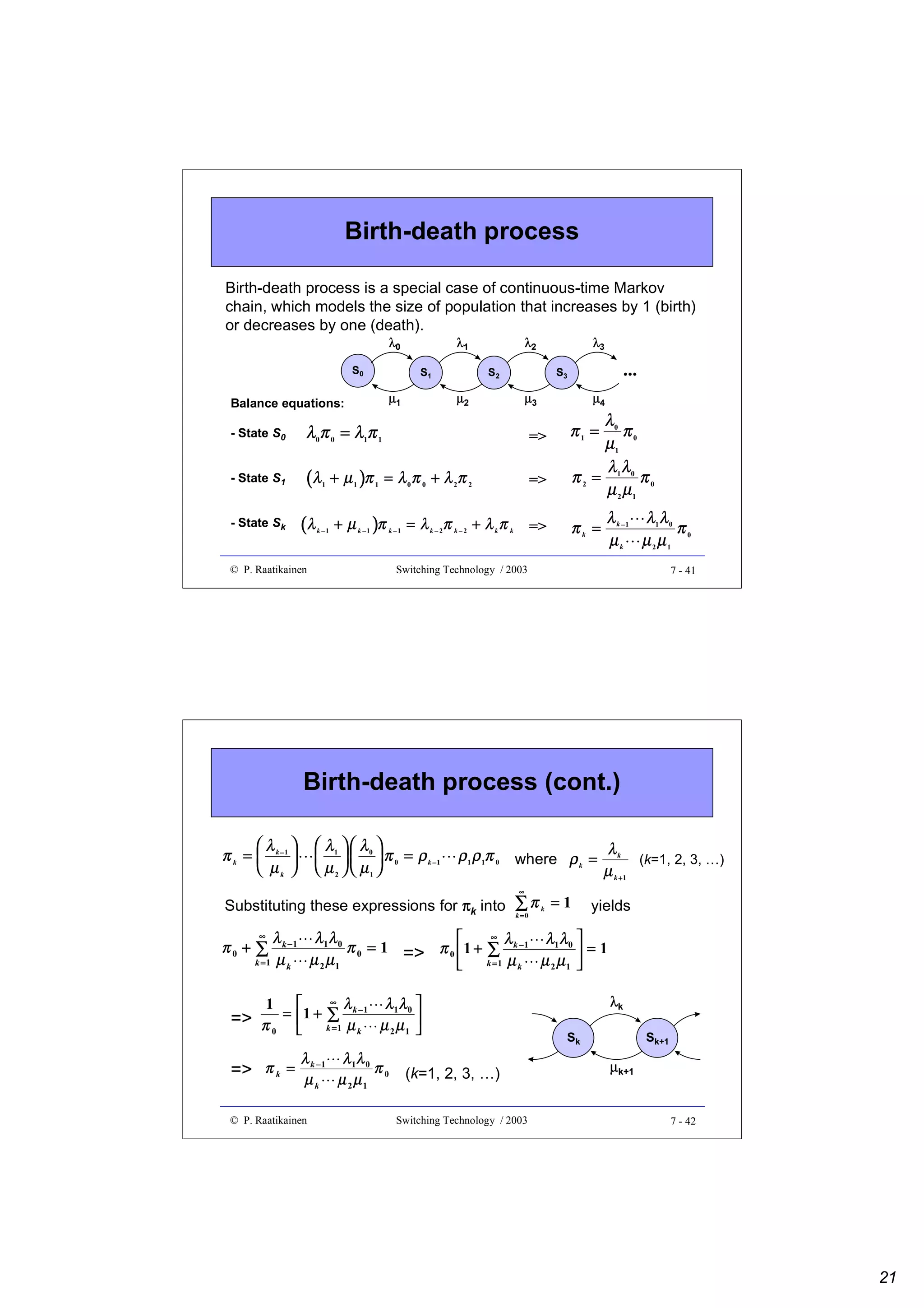
![Markov chain modeling (cont.)
• Probabilities (πi) of the states and transition rates (λij) between the
states are tied together with the following formula
πΛ = 0
where
π n]
)
¡
¡
¢
¡
¡
© P. Raatikainen
)
λ13
λ23
− (λ31 + λ32 +
¢
λ12
− (λ21 + λ23 +
λ32
¢
)
¢
¢
− (λ12 + λ13 +
λ21
Λ=
λ31
¢
π = [π 1 π 2
Switching Technology / 2003
7 - 39
Markov chain modeling (cont.)
Example
λ12
λ13
− (λ12 + λ13 )
Λ=
− (λ21 + λ23 )
λ21
λ23
− (λ31 + λ32 )
λ31
λ32
and π = [π 1 π 2
£
πΛ = 0
πn]
− (λ12 + λ13 )π 1 + λ12π 2 + λ13π 3 = 0
λ21π 1 − (λ21 + λ23 )π 2 + λ23π 3 = 0
λ π + λ π − (λ + λ )π = 0
32 2
31
32
3
31 1
© P. Raatikainen
Switching Technology / 2003
λ12
S1
λ31
S2
λ21
λ13
λ32
λ23
S3
7 - 40
20](https://image.slidesharecdn.com/optix-core-good-140111131404-phpapp02/75/Optical-Switching-Comprehensive-Article-175-2048.jpg)
![Markov chain modeling (cont.)
Chapman-Kolmogorov equations:
∀i , j ∈ S
pij ( t + s ) = ∑ pik ( t ) pkj ( s )
∀s , t ≥ 0
k∈S
Since p(t) is a continuous function
d
pij ( ∆t ) = pij (0 ) + pij ( 0) ∆t + o( ∆t 2 )
dt
d
λij ( t ) = pij (0 )
We have defined =>
dt
≠
For i≠j:
pij ( ∆t ) = pij (0 ) + λij ∆t + o( ∆t 2 ) ≈ λij ∆t
(for small ∆t)
For i=j:
pii ( ∆t ) = pii (0 ) + λii ∆t + o( ∆t 2 ) ≈ 1 + λii ∆t
(for small ∆t)
© P. Raatikainen
Switching Technology / 2003
7 - 49
Markov chain modeling (cont.)
From Chapman-Kolmogorov equations:
pij ( t + ∆t ) = ∑ pik ( t ) pkj ( ∆t ) = pij ( t ) p jj ( ∆t ) + ∑ pik ( t ) pkj ( ∆t )
k≠ j
k
[
]
[
= pij ( t ) 1 + λ jj ∆t + o( ∆t ) + ∑ pik ( t ) λkj ∆t + o( ∆t 2 )
2
k≠ j
]
pij ( t + ∆t ) = pij ( t ) + ∑ pik ( t )λkj ∆t + ∑ pik ( t ) o( ∆t 2 )
k
k
pij ( t + ∆t ) − pij ( t )
∆t
o( ∆ t 2 )
= ∑ pik ( t )λkj + ∑ pik ( t )
k
k
∆t
Taking the limit as ∆t → 0
© P. Raatikainen
d
pij ( t ) = ∑ pik ( t )λkj
dt
k
Switching Technology / 2003
∀i , j
7 - 50
25](https://image.slidesharecdn.com/optix-core-good-140111131404-phpapp02/75/Optical-Switching-Comprehensive-Article-180-2048.jpg)
![Markov chain modeling (cont.)
An alternative derivation of the steady-state conditions begins with
the differential equation describing the process:
d
pij ( t ) = ∑ pik ( t )λkj
dt
k
∀i , j
Suppose that we take the limit of each side as t → ∞
d
pij (t ) = lim ∑ pik (t )λkj
t →∞
dt
k
=>
lim
=>
d
lim pij (t ) = ∑ lim pik (t )λkj
t →∞
dt t →∞
k
=>
∑π
t →∞
k
λkj = 0
i.e. πΛ=0
k
© P. Raatikainen
Switching Technology / 2003
7 - 55
Markov chain modeling (cont.)
Example
λ12
λ13
− (λ12 + λ13 )
Λ=
− (λ21 + λ23 )
λ21
λ23
− (λ31 + λ32 )
λ31
λ32
and π = [π 1 π 2
πΛ = 0
πn]
λ12
S1
λ31
S2
λ21
λ13
λ32
λ23
S3
− (λ12 + λ13 )π 1 + λ21π 2 + λ31π 3 = 0
λ12π 1 − (λ21 + λ23 )π 2 + λ32π 3 = 0
λ π + λ π − (λ + λ )π = 0
23 2
31
32
3
13 1
© P. Raatikainen
Switching Technology / 2003
7 - 56
28](https://image.slidesharecdn.com/optix-core-good-140111131404-phpapp02/75/Optical-Switching-Comprehensive-Article-183-2048.jpg)
![MTIE limits for PRC, SSU and SEC
Clock
source
Time-slot
interval [ns]
Time-slot
interval [ns]
PRC
25 ns
0.3t ns
300 ns
0.01t ns
0.1 < t < 83 s
83 < t < 1000 s
1000 < t < 30 000 s
t > 30 000 s
SSU
25 ns
10t ns
2000 ns
433t0.2 + 0.01t ns
0.1 < t < 2.5 s
2.5 < t < 200 s
200 < t < 2 000 s
t > 2 000 s
SEC
250 ns
100t ns
2000 ns
433t0.2 + 0.01t ns
0.1 < t < 2.5 s
2.5 < t < 20 s
20 < t < 2 000 s
t > 2 000 s
ETS 300 462-3
© P. Raatikainen
Switching Technology / 2003
8 - 25
Occurrence of slips
• Slips occur on connections whose timing differs from the timing signal used by
the exchange
• If both ends of a connection are internally synchronized to a PRC signal,
theoretically slips occur no more frequently than once in 72 days
• In a reference connection a slip occurs theoretically once in 72/12 = 6 days
or if national segments are synchronized once in 720/4 = 18 days
• Slip requirement on an end-to-end connection is looser:
Average frequency of slips
Share of time during one year
≤ 5 slips / 24h
98.90 %
5 slips/ 24 h …. 30 slips/ 1h
<1%
≤ 10 slips / 1h
< 0.1 %
© P. Raatikainen
Switching Technology / 2003
8 - 26
13](https://image.slidesharecdn.com/optix-core-good-140111131404-phpapp02/75/Optical-Switching-Comprehensive-Article-196-2048.jpg)
![Slip calculation example
Show that two networks with single frame buffers and timed from
separate PRCs would see a maximum slip rate of one slip every
72 days
Solution:
• Timing accuracy of a PRC clock is 10-11
• Let the frequencies of the two ends be f1 and f2
• In the worst case, these frequencies deviate from the reference
clock fo by 10-11x fo and those deviations are to different directions
• Let the frequencies be f1 = (1+ 10-11) fo and f2 = (1- 10-11) fo
• Duration of bits in these networks are T1= 1/ f1 and T2= 1/ f2
© P. Raatikainen
Switching Technology / 2003
8 - 27
Slip calculation example (cont.)
Solution (cont.):
• During one bit interval, the timing difference is T1- T2 and after
some N bits the difference exceeds a frame length of 125 µs and a
slip occurs => NT1- T2 = 125x10-9
-9 /[(1/ f -1/ f ) ]
=> N = 125x10
1
2
• Inserting f1 = (1+ 10-11) fo and f2 = (1- 10-11) fo into the above equation,
we get => N = 125x10-9 fo (1- 10-22)/(2x 10-11)
• Multiplying N by the duration (Tb) of one bit , we get the time (Tslip)
between slips
• In case of E1 links, fo= 2.048x10⁶/s and Tb = 488 ns. Dividing the
obtained Tslip by 60 (s), then by 60 (min) and finally by 24 (h) we get
the average time interval between successive slips to be 72.3 days
© P. Raatikainen
Switching Technology / 2003
8 - 28
14](https://image.slidesharecdn.com/optix-core-good-140111131404-phpapp02/75/Optical-Switching-Comprehensive-Article-197-2048.jpg)
![PDH bit rates and related bit/octet times
Hierarchy
level
Time-slot
Bit interval
interval [ns]
[ns]
E1/2M
3906
488
E2/8M
947
118
E3/34M
233
29
E4/140M
57.4
7.2
• When time-slots turn into parallel form (8 bits in parallel) memory
speed requirement decreased by a factor of 8
• Present day memory technology enables up to 256 PDH E1 signals
to be written to and read from a SRAM memory on wire speed
© P. Raatikainen
Switching Technology / 2003
8 - 35
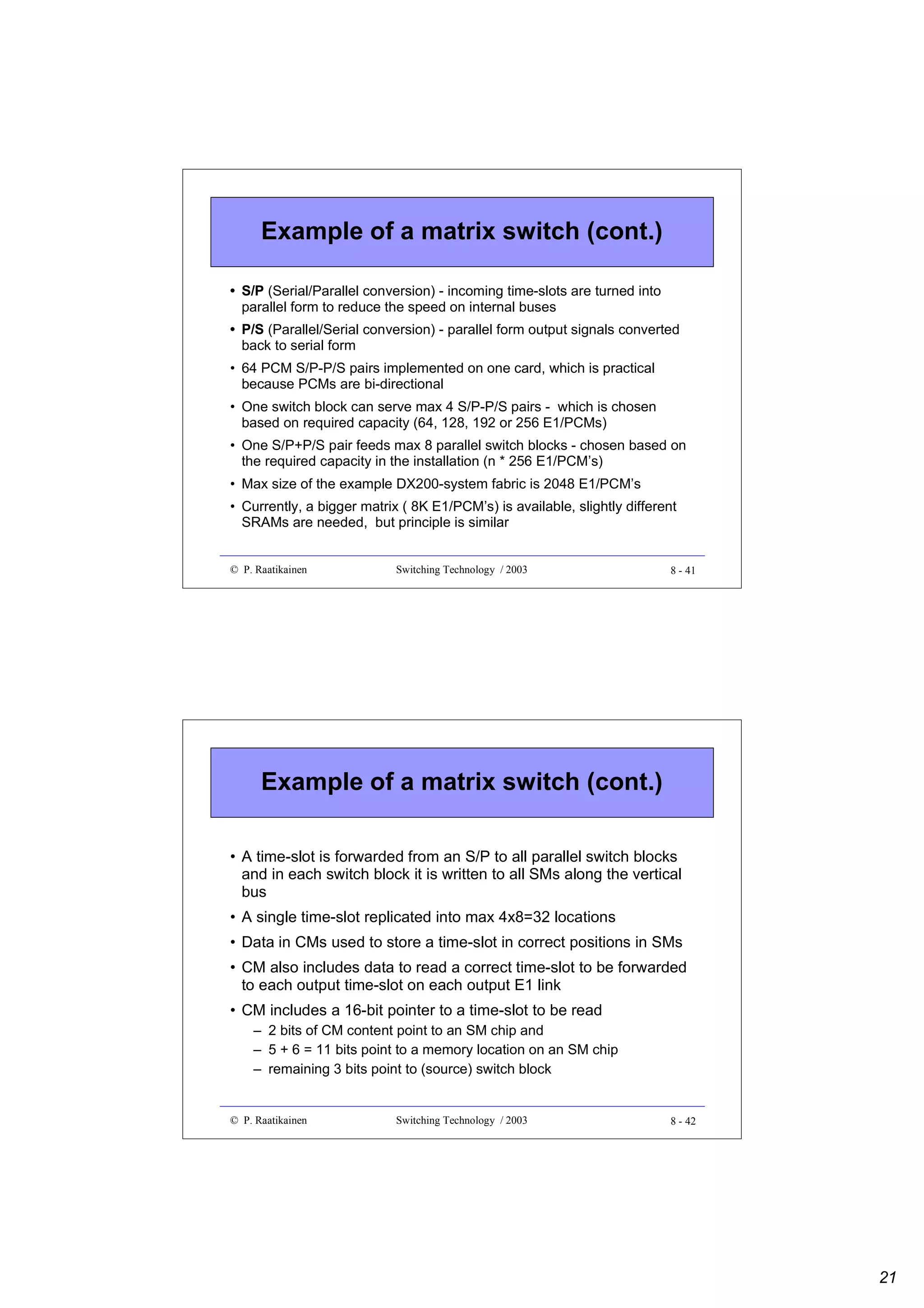
Properties of full matrix switches
Pros
• strict-sense non-blocking
• no path search - a connection can always be written into the
control memory if requested output is idle
• multi-cast capability
• constant delay
• multi-slot connections possible
Cons
• switch and control memory both increase in square of the number
of input/outputs
• broadband - required memory speed may not be available
© P. Raatikainen
Switching Technology / 2003
8 - 36
18](https://image.slidesharecdn.com/optix-core-good-140111131404-phpapp02/75/Optical-Switching-Comprehensive-Article-201-2048.jpg)

![New directions in IP lookup
• More efficient lookup schemes have been developed to improve the
average lookup performance and storage complexity
• Examples of new methods are
• Binary search on trie levels, which decomposes the longest prefix
operation into W exact matching operations, each performed on prefixes
of equal length
• Multiway or K-way range search, which applies a binary search to best
matching prefixes by using two routing entries per prefix and with some
precomputation
• Ternary CAM uses a special CAM (Content Addressable Memory),
which performs parallel comparisons internally. TCAM stores each W-bit
field as a [val, mask] pair and when a bit string is presented to the input,
TCAM outputs the location (or address) where a match is found.
© P. Raatikainen
Switching Technology / 2005
L10 - 65
New directions in IP lookup (cont.)
• Conventional routers offer the best-effort service by processing each
incoming packet in the same way. New applications require different
QoS levels and to meet these requirements new mechanisms, such
as admission control, resource reservation and per-flow queuing,
need to be implemented in routers.
• Routers are required to distinguish and classify incoming traffic into
different flows
• Flows are specified by rules and each rule consists of operations for
comparing packet fields with certain values
• Packet fields to be inspected are collected from different protocols
=> packet classification
© P. Raatikainen
Switching Technology / 2005
L10 - 66](https://image.slidesharecdn.com/optix-core-good-140111131404-phpapp02/75/Optical-Switching-Comprehensive-Article-272-2048.jpg)
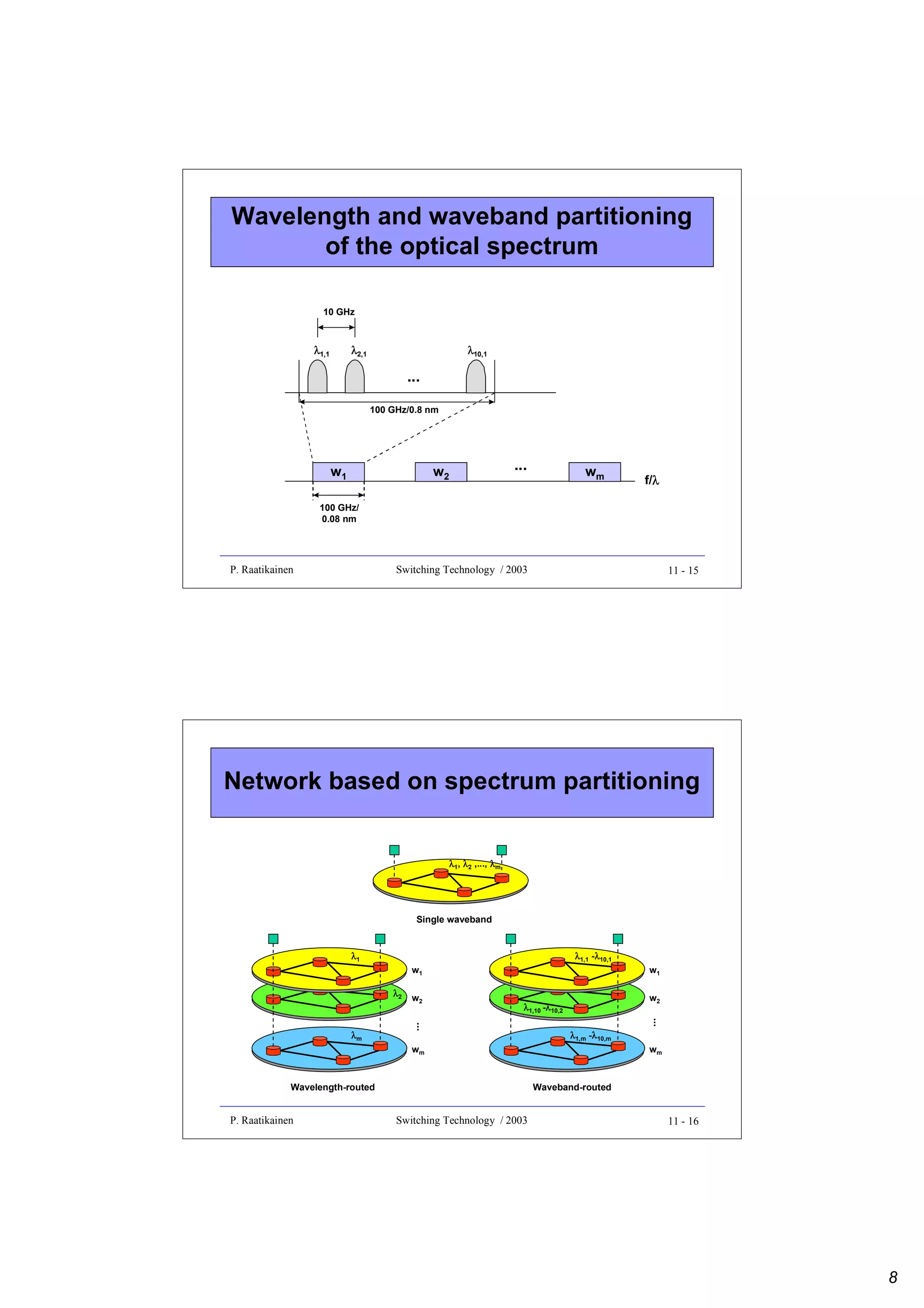
![Optical spectrum
• Since wavelength λ and frequency f are related by f λ = c, where c is the
velocity of light in the medium, we have the relation
∆ f ≈ − c ∆λ
2
λ
• Thus, 10 GHz ≈ 0.08 nm and 100 GHz ≈ 0.8 nm in the range of 1,550 nm,
where most modern lightwave networks operate
• The 10-GHz channel spacing is sufficient to accommodate λ-channels
carrying aggregate digital bit rates on the order of 1 Gbps
- modulation efficiency of 0.1 bps/Hz typical for optical systems
• The 10-GHz channel spacing is suitable for optical receivers, but much too
dense to permit independent wavelength routing at the network nodes
- for this, 100-GHz channel spacing is needed.
• In a waveband routing network, several λ-channels (with 10-GHz channel
spacing) comprise an independently routed waveband (with 100-GHz
spacing between wavebands).
P. Raatikainen
Switching Technology / 2003
11 - 13
Wavelength partitioning of the optical
spectrum
Unusable spectrum
λ1
λ2
λm
...
λ
f/λ [GHz/nm]
10 GHz
0.08 nm
λ-channel spacing for separability at receivers
λ1
λ2
λm
...
f/λ
λ
100 GHz/0.8 nm
λ-channel spacing for separability at network nodes
P. Raatikainen
Switching Technology / 2003
11 - 14
7](https://image.slidesharecdn.com/optix-core-good-140111131404-phpapp02/75/Optical-Switching-Comprehensive-Article-280-2048.jpg)
![Directional Coupler (1)
• Directional coupler (= 2x2 switch) is an optical four-port
– ports 1 and 2 designated as input ports
– ports 1’ and 2’ designated as output ports
• Optical power
– enters a coupler through fibers attached to input ports,
– divided and combined linearly
– leaves via fibers attached to output ports
• Power relations for input signal powers
powers P1′ and P2′ are given by
P1 and P2 and output
P ′ = a11 P + a12 P2
1
1
P2′ = a21 P + a22 P2
1
1
• Denote the power transfer matrix by A
P. Raatikainen
= [aij]
2
a11
a21
a12
1′
2′
a22
Switching Technology / 2003
11 - 27
Directional Coupler (2)
• Ideally, the power transfer matrix A is of the form
1 − α
A=
α
α
,
1−α
0 ≤α ≤1
• If parameter α is fixed, the device is static, e.g. with α = 1/2 and
signals present at both inputs, the device acts as a 2x2 star coupler
• If α can be varied through some external control, the device is
dynamic or controllable, e.g. add-drop switch
• If only input port 1 is used (i.e., P2 = 0),
1
the device acts as a 1x2 divider
• If only output port 1’ is used (and port 2’ is
2
terminated), the device acts as a 2x1 combiner
P. Raatikainen
Switching Technology / 2003
1−α
α
α
1−α
1′
2′
11 - 28
14](https://image.slidesharecdn.com/optix-core-good-140111131404-phpapp02/75/Optical-Switching-Comprehensive-Article-287-2048.jpg)
![Permutation switch
P. Raatikainen
1′
2′
3′
4′
output ports
1′ 2′ 3′ 4′
input ports
1
• Dynamic NxN permutation switch
(e.g. crossbar switch)
2
– unicast optical connections
3
between input and output ports
4
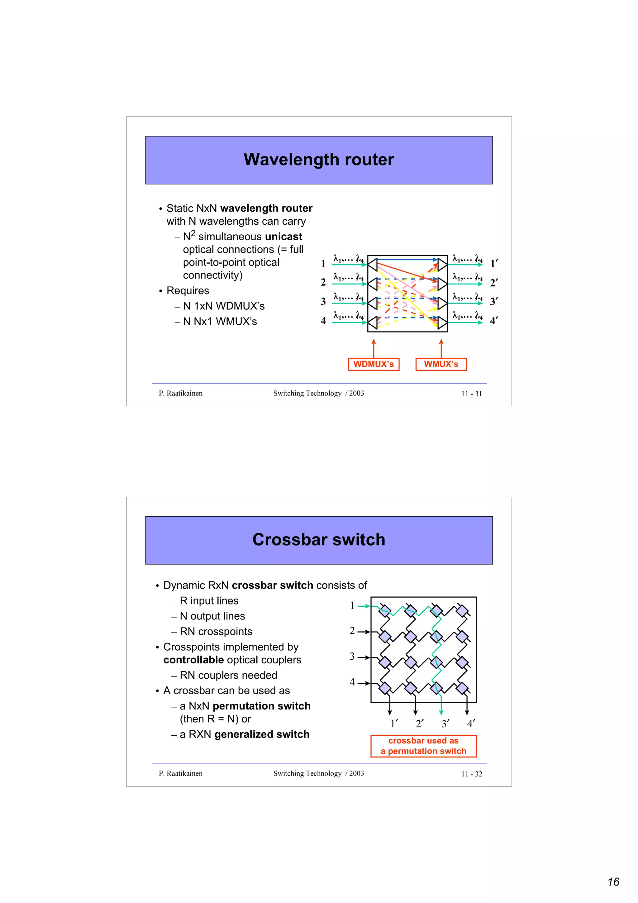
– N! connection states (if
nonblocking)
– each connection state can carry N
simultaneous unicast optical
connections
– representation of a connection state
by a NxN connection matrix
1
1
2 1
3
1
4
1
Switching Technology / 2003
11 - 33
Generalized switch
• Dynamic RxN generalized switch (e.g.
crossbar switch)
1/N
1/N
1/N
1/N
1
– any input/output pattern possible
2
– 2NR connection states
3
– each connection state can carry (at most)
R simultaneous multicast optical
4
connections
– a connection state represented by a RxN
connection matrix
1 ,
aij = NR
0,
P. Raatikainen
if switch (i,j ) is on
otherwise
Switching Technology / 2003
2′
3′
4′
output ports
1′ 2′ 3′ 4′
input ports
• Input/output power relation P’ = AP with
NxR power transfer matrix A = [aij], where
1/R1/R
1/R
1/R
1′
1
1 1
2 1
1
3
1
4 1 1 1
11 - 34
17](https://image.slidesharecdn.com/optix-core-good-140111131404-phpapp02/75/Optical-Switching-Comprehensive-Article-290-2048.jpg)
![Linear Divider-Combiner (LDC)
1′
1
δ11
• Linear Divider-Combiner (LDC) is
δ δ21
δ41 31
a generalized switch that
2
– controls power-dividing and
power-combining ratios
3
σ41
– less inherent loss than in crossbar
σ σ42
σ4443
4
• Power-dividing and power-combining ratios
– δij = fraction of power from input port j directed to output port i’
– σij = fraction of power from input port j combined onto output port i
• In an ideal case of lossless couplers, we have constraints
2′
3′
4′
∑ δ ij = 1 and ∑ σ ij = 1
i
j
• The resulting power transfer matrix A = [aij] is such that
aij = δ ijσ ij
P. Raatikainen
Switching Technology / 2003
11 - 35
LDC and generalized switch realizations
1
rx1
combiner
directional couplers
11
12
1r
...
22
2r
...
21
2
1xn
splitter
n
...
δ - σ linear divider-combiner
1
2
n1
r
n2
nr
Generalized optical switch
P. Raatikainen
Switching Technology / 2003
11 - 36
18](https://image.slidesharecdn.com/optix-core-good-140111131404-phpapp02/75/Optical-Switching-Comprehensive-Article-291-2048.jpg)
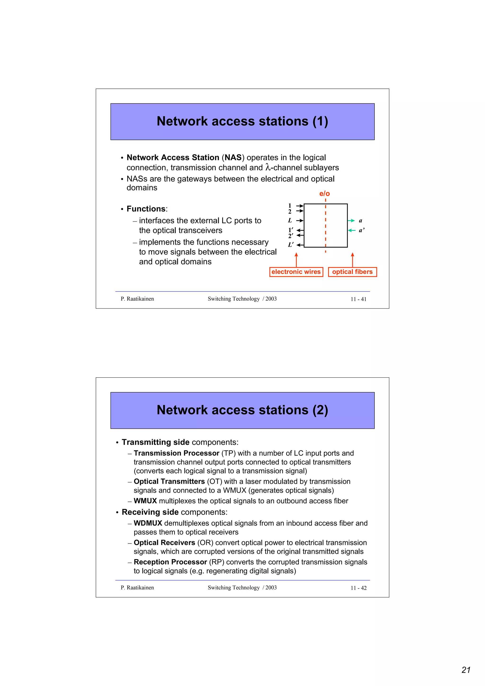
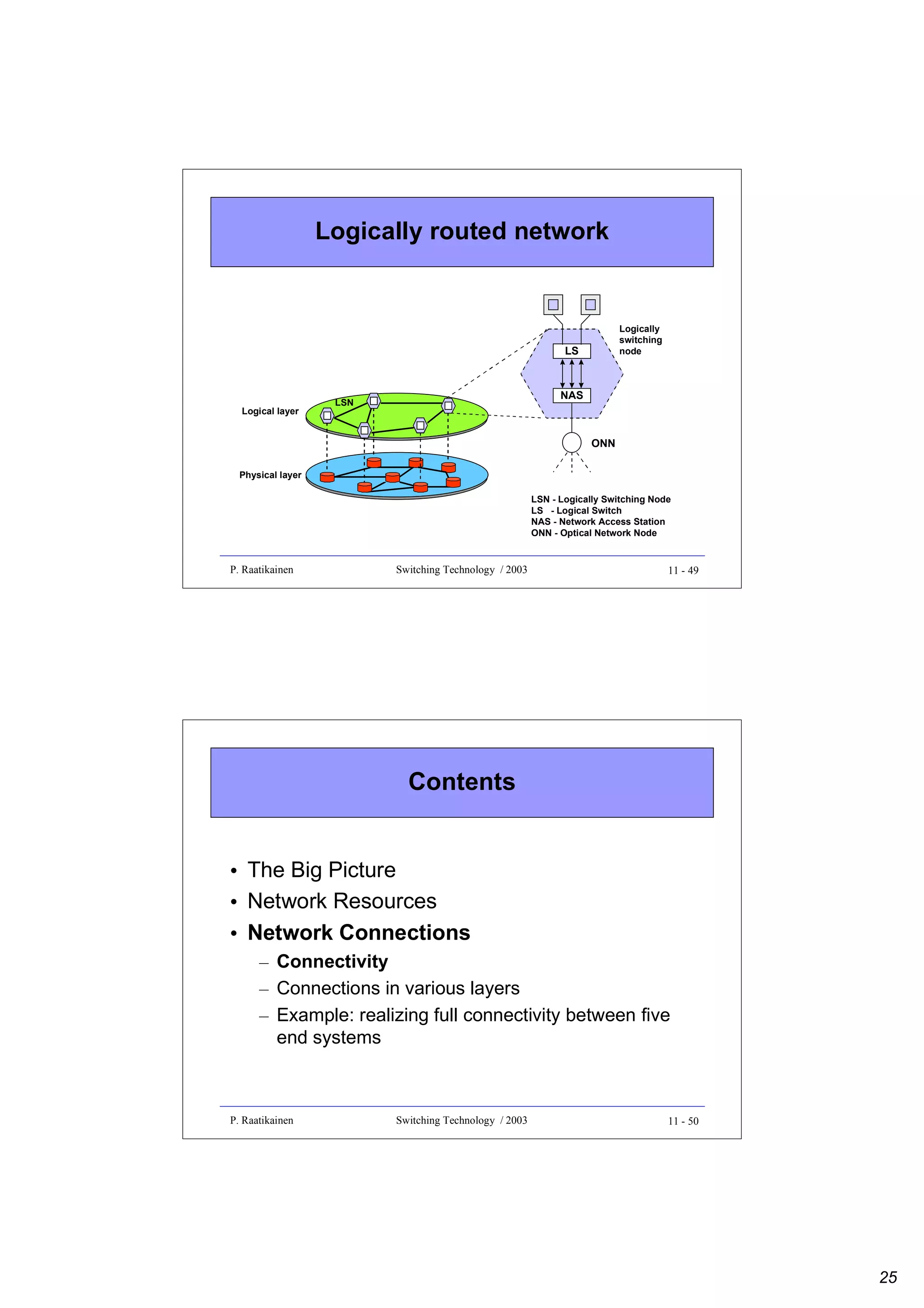
![Connections in various layers
• Logical connection sublayer
– Logical connection (LC) is a unidirectional connection between
external ports on a pair of source and destination network
access stations (NAS)
• Optical connection sublayer
– Optical connection (OC) defines a relation between one
transmitter and one or more receivers, all operating in the same
wavelength
• Optical path sublayer
– Optical path (OP) routes the aggregate power on one waveband
on a fiber, which could originate from several transmitters within
the waveband
P. Raatikainen
Switching Technology / 2003
11 - 55
Notation for connections in various
layers
• Logical connection sublayer
– [a, b] = point-to-point logical connection from an external port on station a
to one on station b
– [a, {b, c, …}] = multi-cast logical connection from a to set {b, c, …}
• station a sends the same information to all receiving stations
• Optical connection sublayer
– (a, b) = point-to-point optical connection from station a to station b
– (a, b)k = point-to-point optical connection from a to b using wavelength λk
– (a,{b,c,…}) = multi-cast optical connection from a to set {b,c,…}
• Optical path sublayer
– 〈a, b〉 = point-to-point optical path from station a to station b
– 〈a, b〉k = point-to-point optical path from a to b using waveband wk
– 〈a, {b, c, …}〉 = multi-cast optical path from a to set {b,c,…}
P. Raatikainen
Switching Technology / 2003
11 - 56
28](https://image.slidesharecdn.com/optix-core-good-140111131404-phpapp02/75/Optical-Switching-Comprehensive-Article-301-2048.jpg)
![Example of a logical connection between
two NASs
Logical connection [A,B]
NAS
NAS
TP
RP
Transmission channel
Electrical
Optical connection (A,B)λ1
OT
Optical
λ-channel
λ1 ... λm
WMUX
Electrical
OR
λm ... λ1
Optical
WDMUX
Optical path <A,B>w1
w1
ONN
w2
P. Raatikainen
ONN
ONN
Switching Technology / 2003
11 - 57
Contents
• The Big Picture
• Network Resources
• Network Connections
– Connectivity
– Connections in various layers
– Example: realizing full connectivity between
five end systems
P. Raatikainen
Switching Technology / 2003
11 - 58
29](https://image.slidesharecdn.com/optix-core-good-140111131404-phpapp02/75/Optical-Switching-Comprehensive-Article-302-2048.jpg)
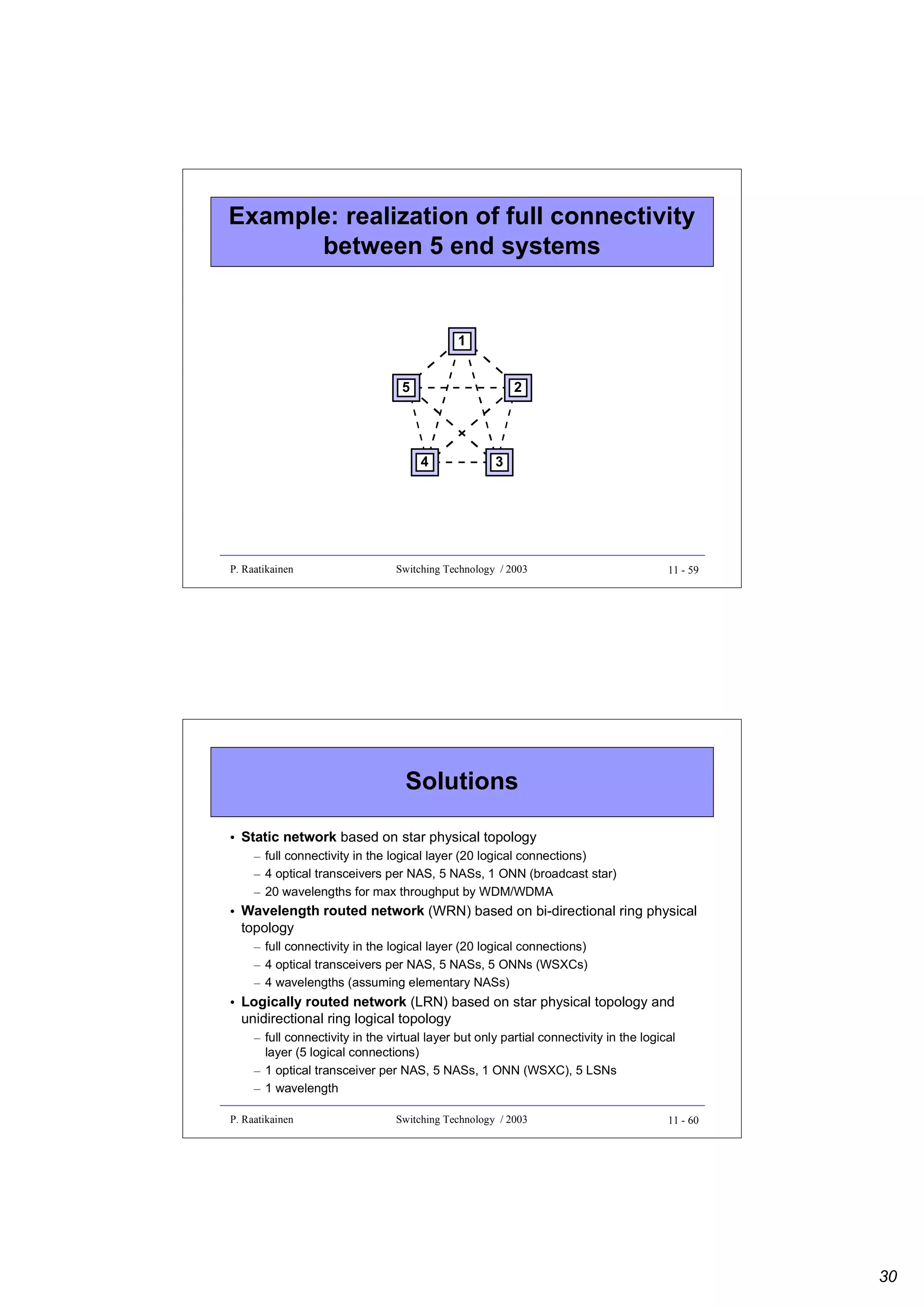
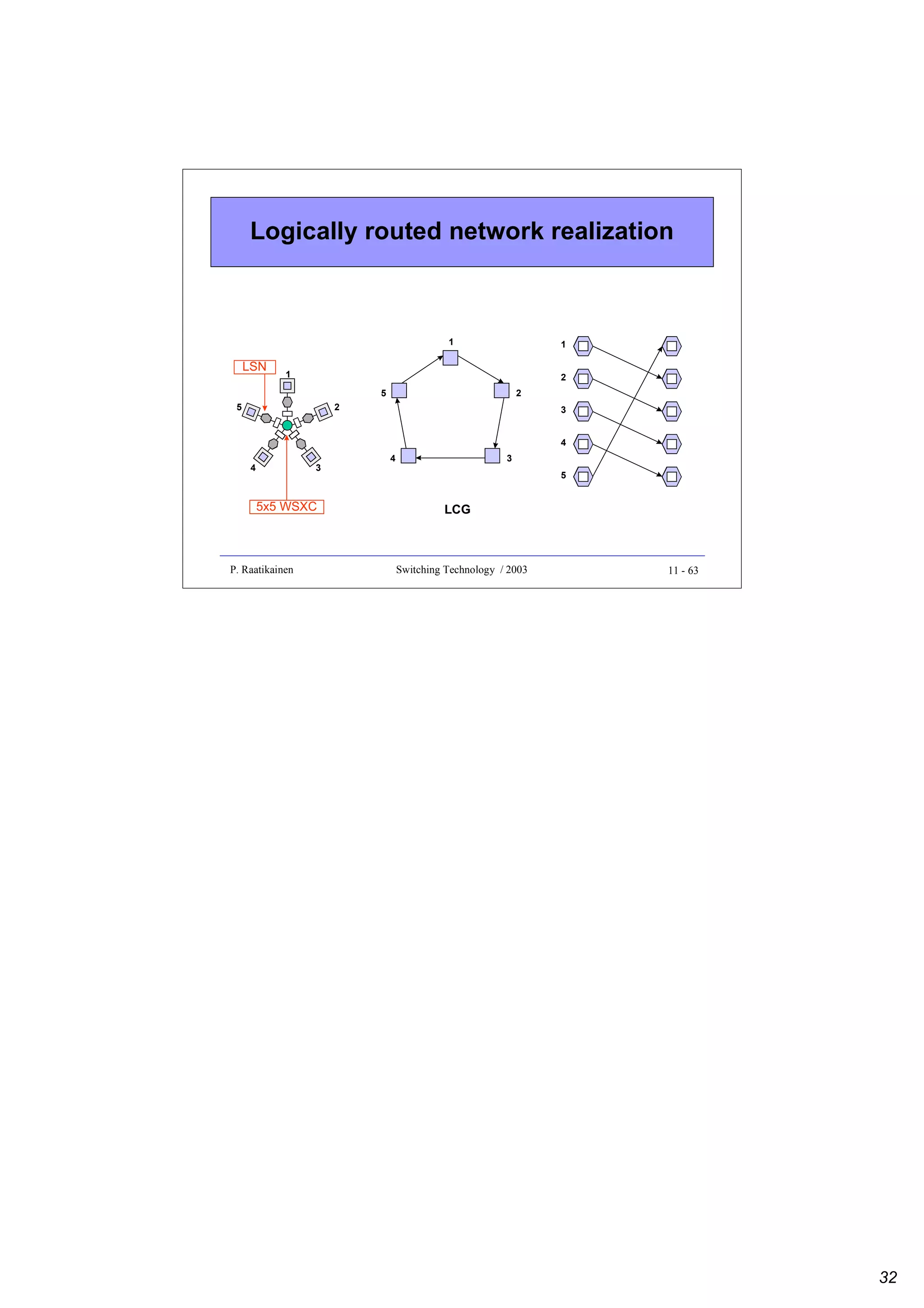
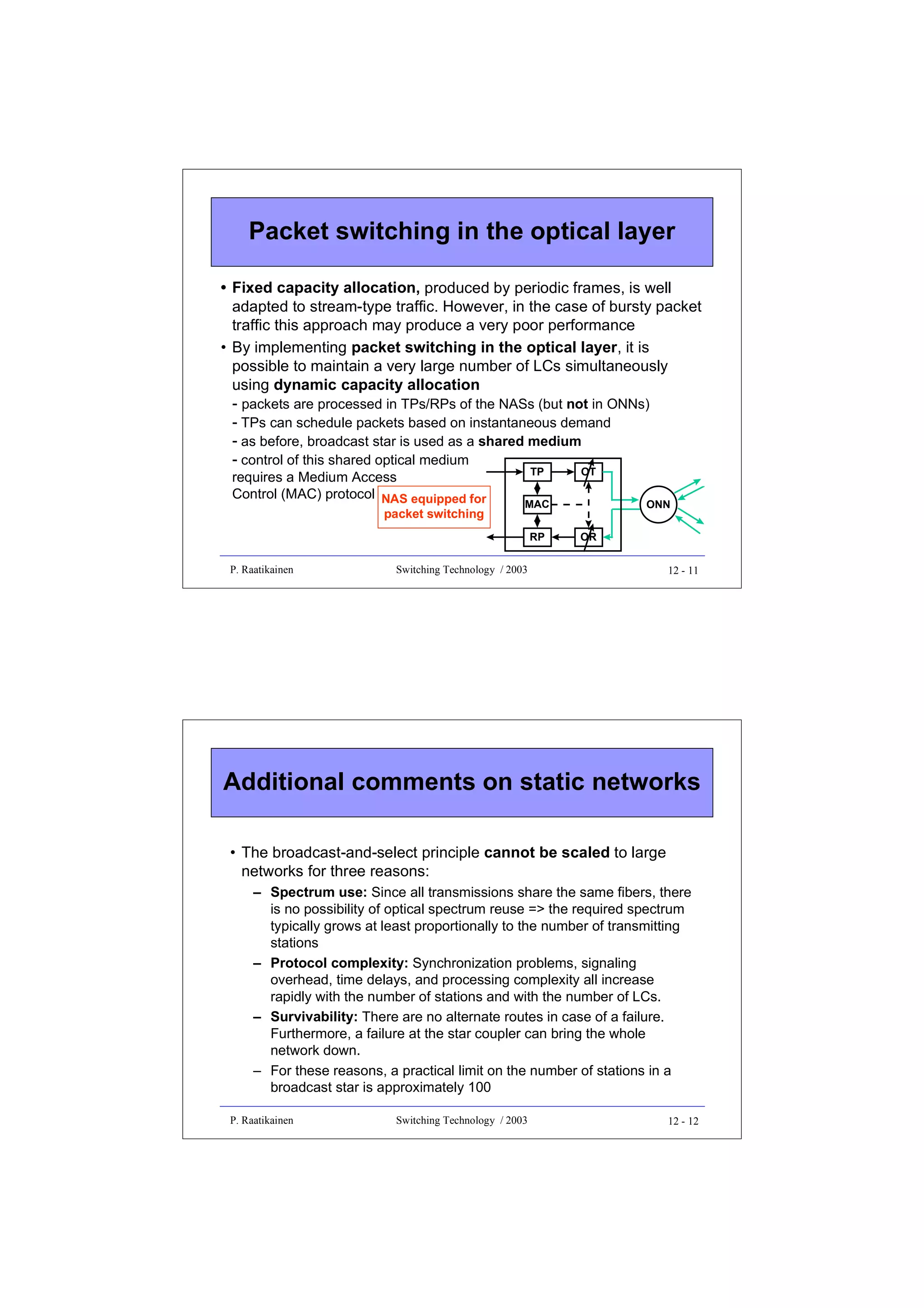
![Static networks
• Static network, also called broadcast-and-select network, is a
purely optical shared medium network
• passive splitting and combining nodes are interconnected by fibers to
provide static connectivity among some or all OTs and ORs
• OTs broadcast and ORs select
• Broadcast star network is an example of such a static network
• star coupler combines all signals and broadcasts them to all ORs
- static optical multi-cast paths from any station to the set of all stations
- no wavelength selectivity at the network node
• optical connection is created by tuning the source OT and/or destination
OR to the same wavelength
• two OTs must operate at different wavelengths (to avoid interference)
- this is called the distinct channel assignment (DCA) constraint
• however, two ORs can be tuned to the same wavelength
- by this way, optical multi-cast connections are created
P. Raatikainen
Switching Technology / 2003
12 - 3
Realization of logical connectivity
• Methods to realize full point-to-point logical connectivity in a
broadcast star with N nodes:
• WDM/WDMA
- a whole λ-channel allocated for each LC
- N(N-1) wavelengths needed (one for each LC)
- N-1 transceivers needed in each NAS
• TDM/TDMA
- 1/[N(N-1)] of a λ-channel allocated for each LC
- 1 wavelength needed
- 1 transceiver needed in each NAS
• TDM/T-WDMA
- 1/(N-1) of a λ-channel allocated for each LC
- N wavelengths needed (one for each OT)
- 1 transceiver needed in each NAS, e.g. fixed OT and tunable OR
(FT-TR), or tunable OT and fixed OR (TT-FR)
P. Raatikainen
Switching Technology / 2003
12 - 4](https://image.slidesharecdn.com/optix-core-good-140111131404-phpapp02/75/Optical-Switching-Comprehensive-Article-307-2048.jpg)
![Broadcast star using WDM/WDMA
LCs
[1,2]
[1,3]
[2,1]
[2,3]
[3,1]
[3,2]
LCs
NAS 1
TP
TP
TP
λ1
OT λ
2
OT
λ3
OT λ
4
OT
λ5
OT λ
6
OT
λ1,2
λ1-6
λ3,4
λ1-6
λ1-6
λ5,6
λ3
λ5 OR
OR
λ1
λ6 OR
OR
λ2
λ4 OR
OR
RP
[2,1]
[3,1]
RP
[1,2]
[3,2]
RP
[1,3]
[2,3]
star coupler
P. Raatikainen
Switching Technology / 2003
12 - 5
Broadcast star using TDM/TDMA
LCs
NAS 1
[1,2]
[1,3]
TP
OT
[2,1]
[2,3]
TP
OT
[3,1]
[3,2]
TP
OT
λ1
λ1
λ1
LCs
λ1
λ1
OR
RP
[2,1]
[3,1]
OR
RP
[1,2]
[3,2]
OR
RP
[1,3]
[2,3]
λ1
star coupler
P. Raatikainen
Switching Technology / 2003
12 - 6](https://image.slidesharecdn.com/optix-core-good-140111131404-phpapp02/75/Optical-Switching-Comprehensive-Article-308-2048.jpg)
![Effect of propagation delay on
TDM/TDMA
OT1
[1,2]1
[1,2]2
[1,3]1
[1,2]2
From 1
[2,3]2
From 2
From 1
F1
From 2
From 1
F1
From 2
F1
From 2
F2
From 1
P. Raatikainen
From 2
F2
From 1
OR2
OR3
[1,3]1
[2,3]1
OT2
Coupler
[1,2]1
From 1
A TDM/TDMA schedule
From 2
F2
Switching Technology / 2003
12 - 7
Broadcast star using TDM/T-WDMA in
FT-TR mode
LCs
fixed
[1,2]
[1,3]
TP
OT
[2,1]
[2,3]
TP
OT
[3,1]
[3,2]
TP
OT
NAS 1
λ1
λ2
λ3
tunable
λ1-3
λ1-3
λ1-3
LCs
λ2
λ3 OR
RP
[2,1]
[3,1]
λ1
λ3 OR
RP
[1,2]
[3,2]
λ1
λ2 OR
RP
[1,3]
[2,3]
star coupler
P. Raatikainen
Switching Technology / 2003
12 - 8](https://image.slidesharecdn.com/optix-core-good-140111131404-phpapp02/75/Optical-Switching-Comprehensive-Article-309-2048.jpg)
![Broadcast star using TDM/T-WDMA in
TT-FR mode
LCs
[1,2]
[1,3]
[2,1]
[2,3]
[3,1]
[3,2]
tunable
TP
λ2
OT λ3
TP
λ1
OT λ3
TP
λ1
OT λ2
NAS 1
fixed
λ1
λ2,3
λ1,3
λ1,2
λ1-3
λ1-3
λ1-3
λ2
λ3
LCs
OR
RP
[2,1]
[3,1]
OR
RP
[1,2]
[3,2]
OR
RP
[1,3]
[2,3]
star coupler
P. Raatikainen
Switching Technology / 2003
12 - 9
Channel allocation schedules for circuit
switching
WDM/WDMA
λ1
λ2
λ3
λ4
[1,2] [1,2] [1,2] [1,2]
[1,3] [1,3] [1,3] [1,3]
[2,1] [2,1] [2,1] [2,1]
TDM/T-WDMA with FT-TR
λ1 [1,2] [1,3] [1,2] [1,3]
λ2 [2,3] [2,1] [2,3] [2,1]
λ3 [3,1] [3,2] [3,1] [3,2]
TDM/T-WDMA with TT-FR
λ1 [2,1] [3,1] [2,1] [3,1]
λ2 [3,2] [1,2] [3,2] [1,2]
λ3 [1,3] [2,3] [1,3] [2,3]
[2,3] [2,3] [2,3] [2,3]
λ5 [3,1] [3,1] [3,1] [3,1]
λ6 [3,2] [3,2] [3,2] [3,2]
frame
TDM/TDMA
frame
frame
Channel allocation schedule (CAS) should be
- realizable = only one LC per each OT and time-slot
- collision-free = only one LC per each λ and time-slot
- conflict-free = only one LC per each OR and time-slot
λ1 [1,2] [1,3] [2,1] [2,3] [3,1] [3,2] [1,2] [1,3] [2,1] [2,3] [3,1] [3,2]
frame
P. Raatikainen
Switching Technology / 2003
12 - 10](https://image.slidesharecdn.com/optix-core-good-140111131404-phpapp02/75/Optical-Switching-Comprehensive-Article-310-2048.jpg)
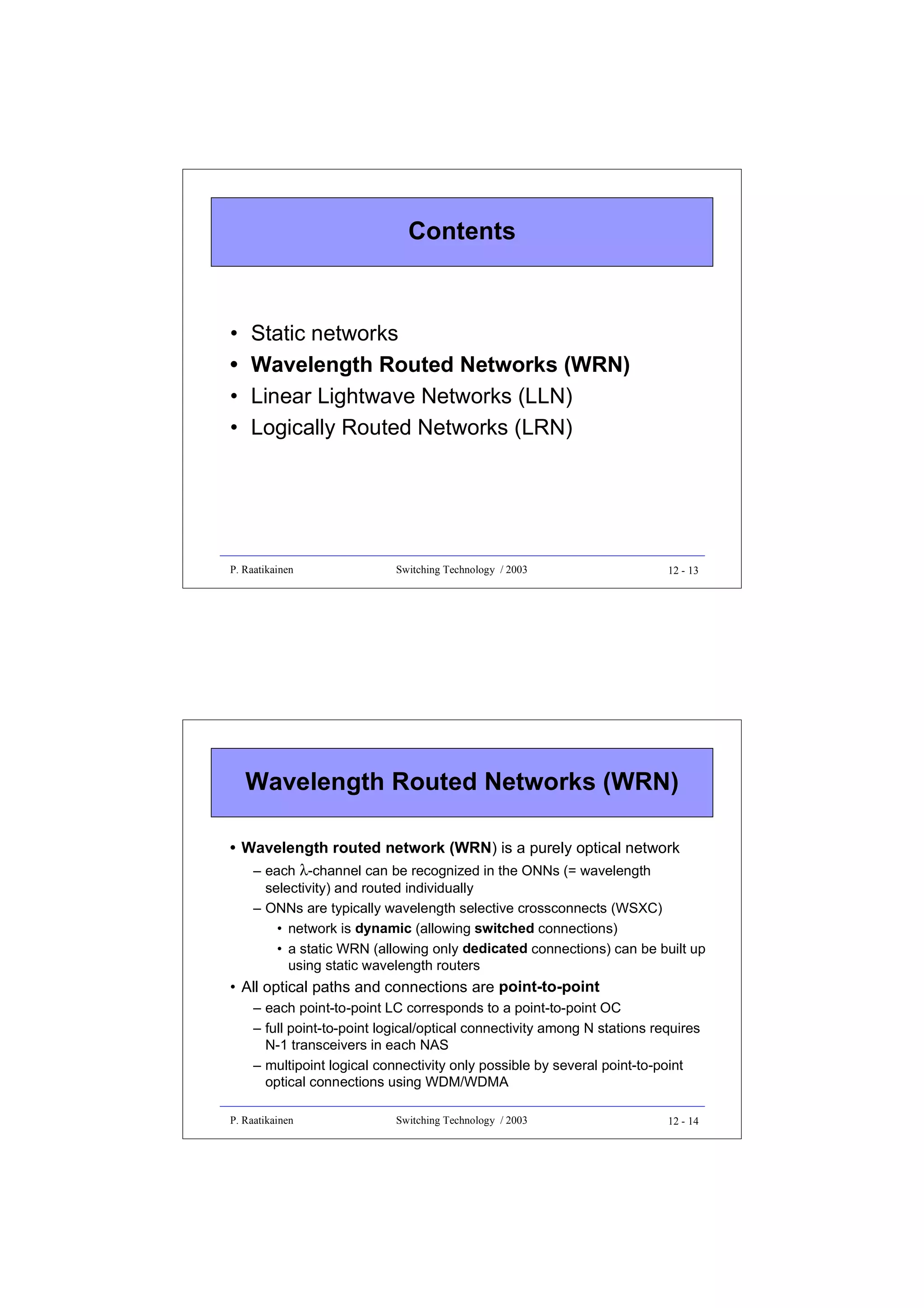
![Static wavelength routed star
• Full point-to-point logical/optical connectivity in a static
wavelength routed star with N nodes can be realized by
– WDM/WDMA
• a whole λ-channel allocated for each LC
• N-1 wavelengths needed
- spectrum reuse factor is N
(= N(N-1) optical connections / N-1 wavelengths)
• N-1 transceivers needed in each NAS
P. Raatikainen
Switching Technology / 2003
12 - 15
Static wavelength routed star using
WDM/WDMA
LCs
NAS 1
[1,2]
[1,3]
TP
[2,1]
[2,3]
TP
[3,1]
[3,2]
TP
λ1
OT λ
2
OT
λ2
OT λ
1
OT
λ1
OT λ
2
OT
λ1,2
λ1,2
λ1,2
LC’
λ1,2
λ1,2
λ1,2
λ2
λ1 OR
OR
λ1
λ2 OR
OR
λ2
λ1 OR
OR
RP
[2,1]
[3,1]
RP
[1,2]
[3,2]
RP
[1,3]
[2,3]
wavelength router
P. Raatikainen
Switching Technology / 2003
12 - 16](https://image.slidesharecdn.com/optix-core-good-140111131404-phpapp02/75/Optical-Switching-Comprehensive-Article-313-2048.jpg)

This document outlines an optics switching technology course, including: - The course covers switching technology, including understanding switching systems, fabrics, implementations, and optical switching. - The schedule lists 13 lectures and 7 exercises over 14 weeks, covering topics such as switch fabrics, PDH, ATM, and optical networks. - Readings are provided to supplement the lecture materials, and requirements include exercises, a grading system, and a final examination.


![Vibe Coding vs. Spec-Driven Development [Free Meetup]](https://cdn.slidesharecdn.com/ss_thumbnails/vibecodingvsspecdrivendevelopment-251209105622-43f455e7-thumbnail.jpg?width=640&height=640&fit=bounds)


