Downloaded 685 times
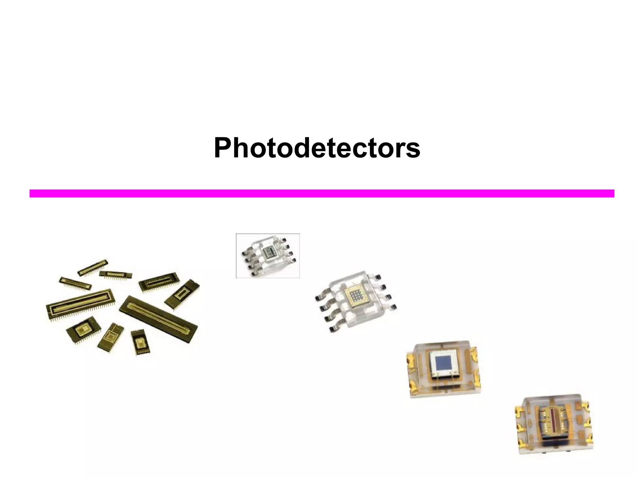
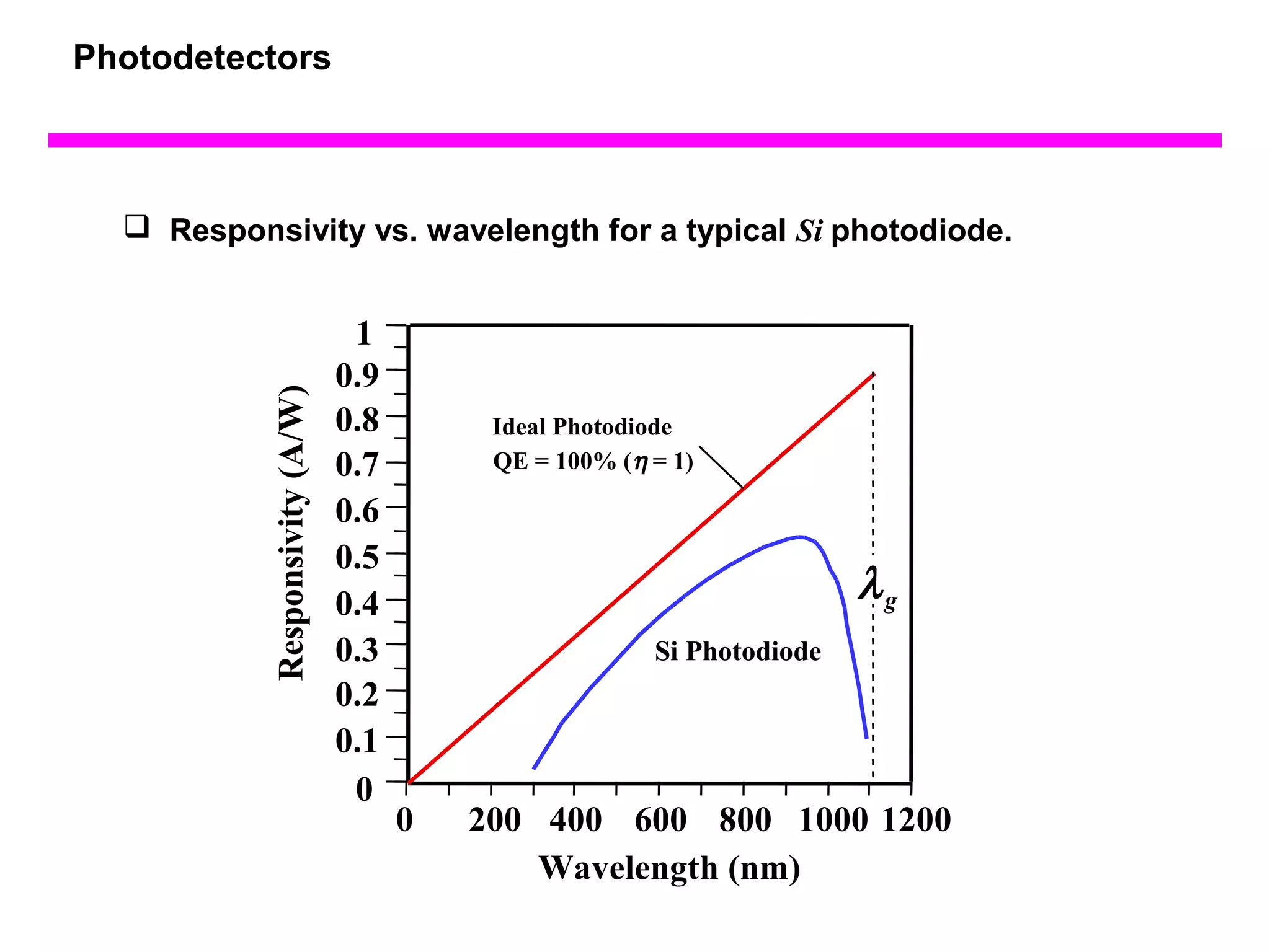
![Photodetectors
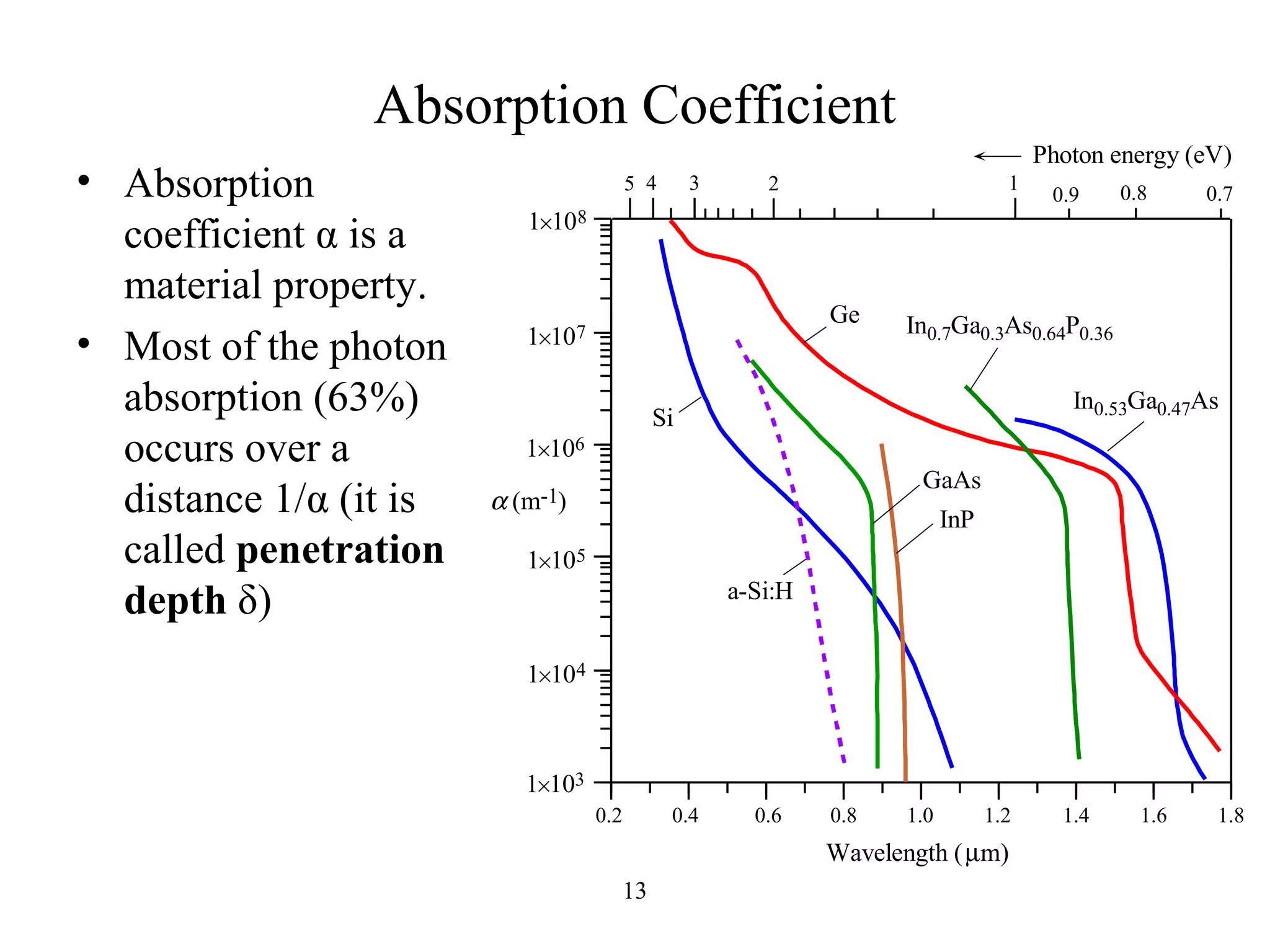
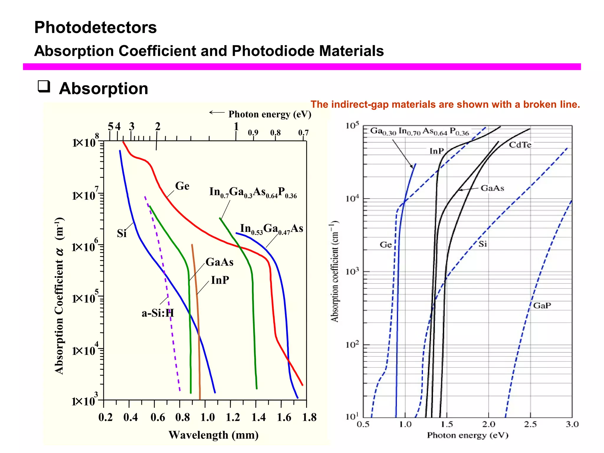
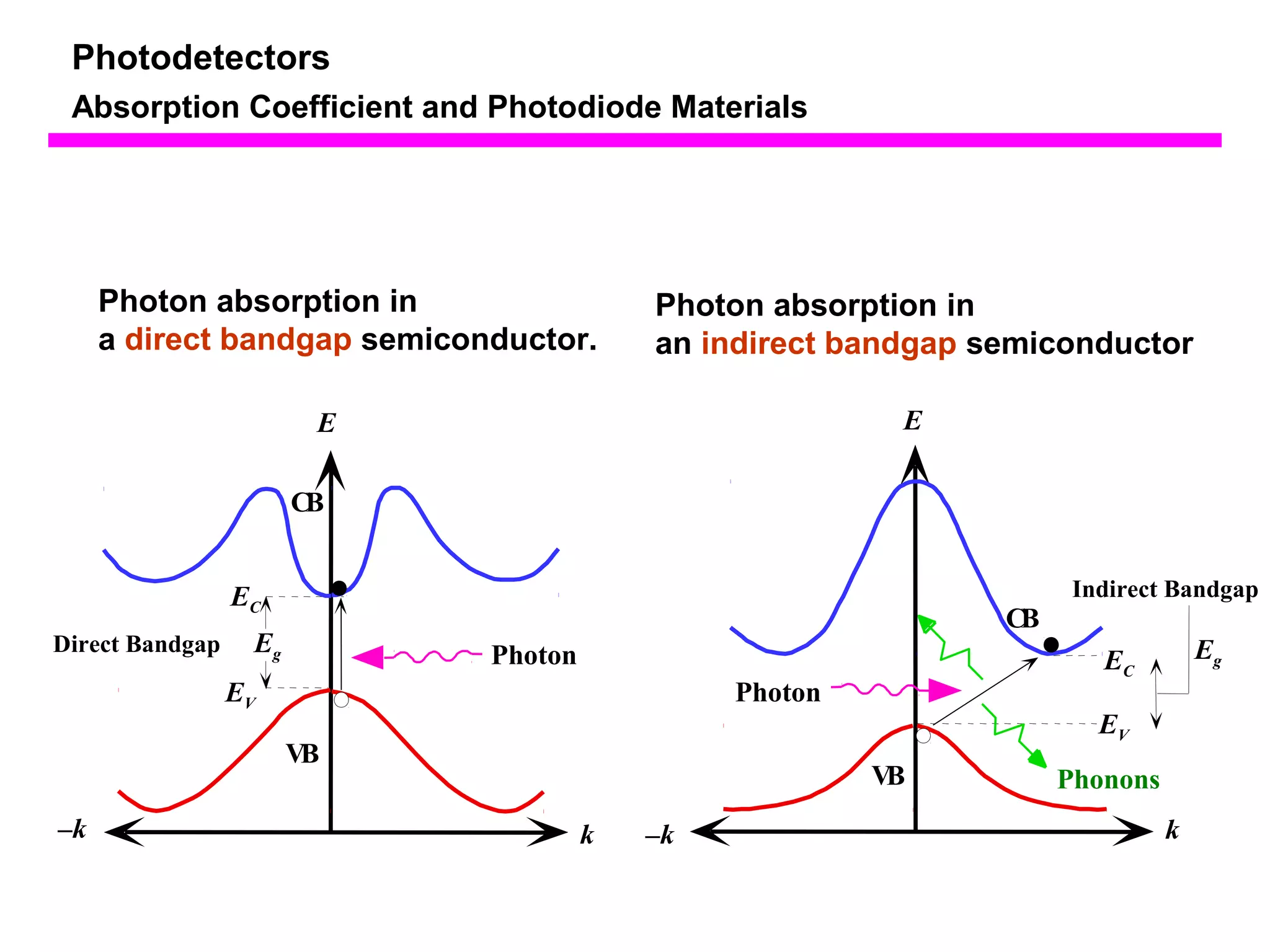
Absorption Coefficient and Photodiode Materials
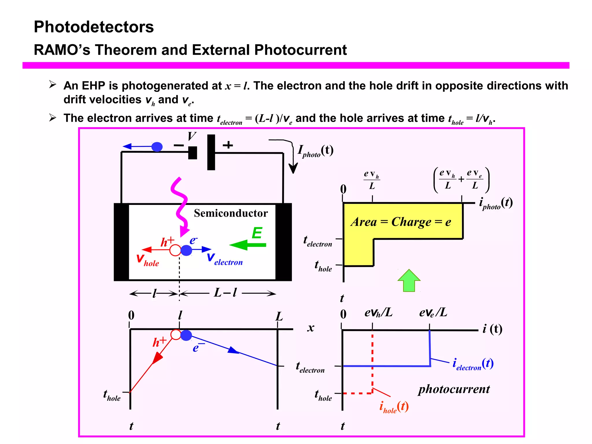
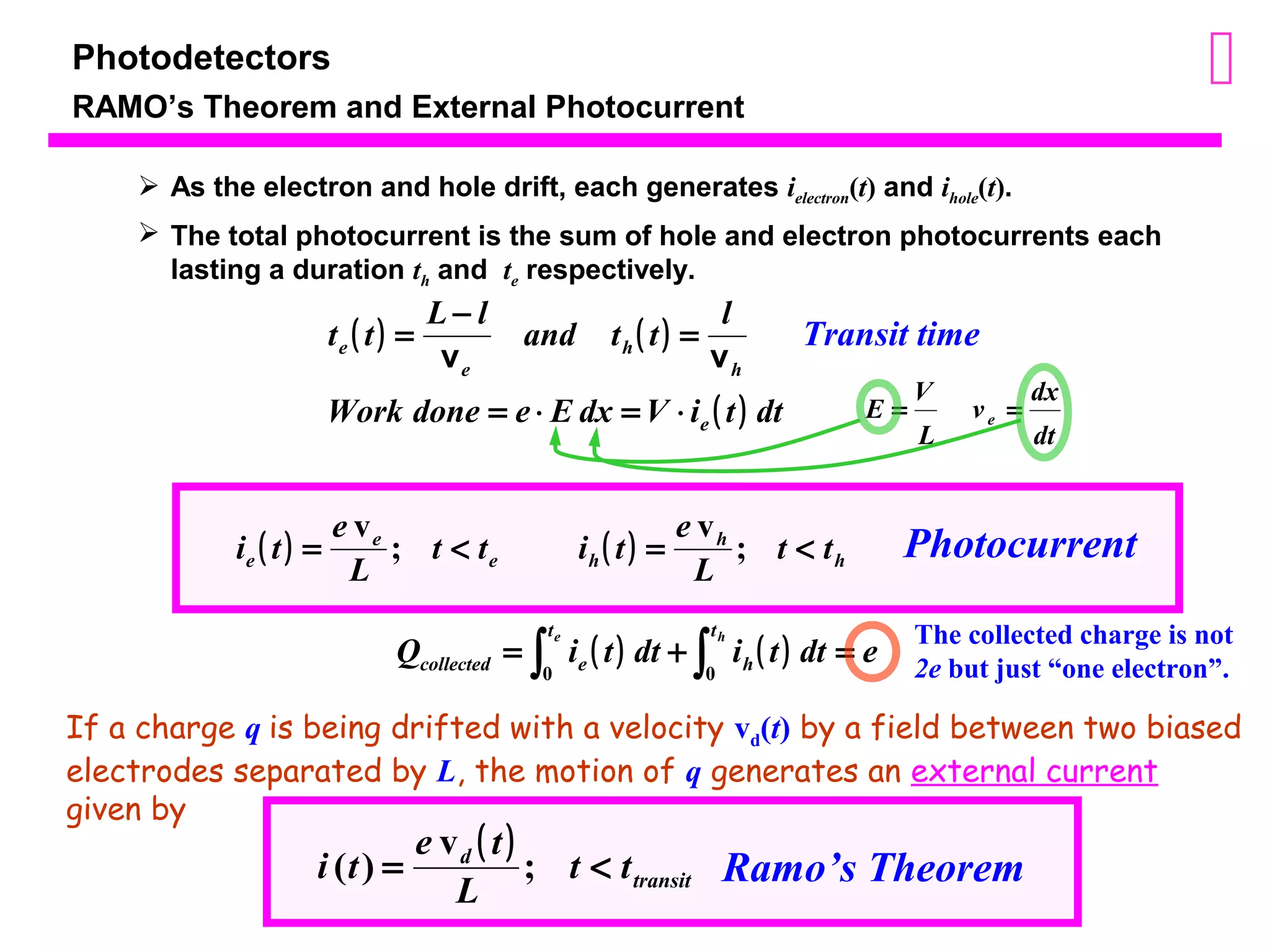
Absorbed Photon create Electron-Hole Pair.
[ ] 1.24 m E eV
[ ]
g
g l m =
Cut-off wavelength
vs. Energy bandgap
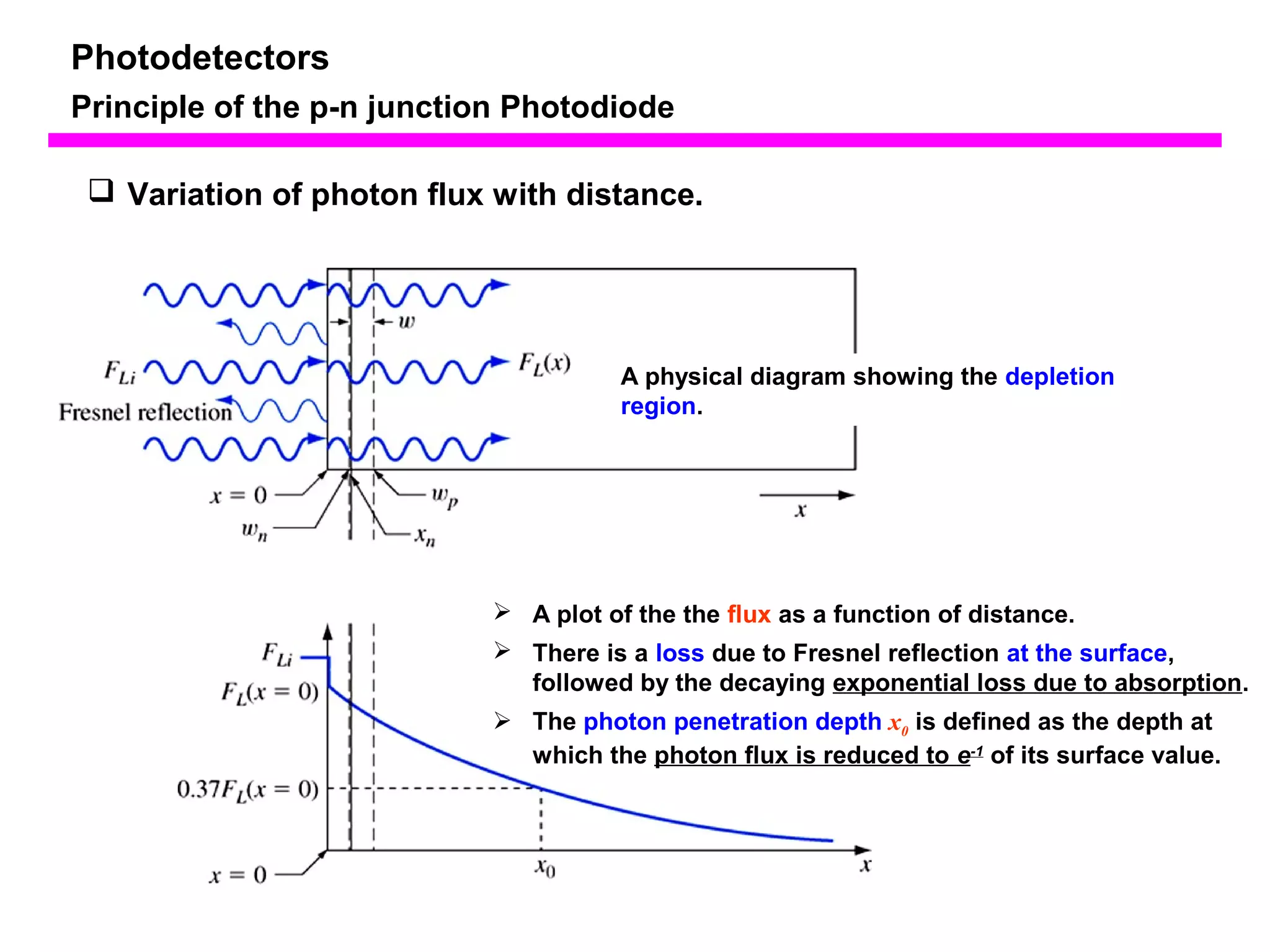
Incident photons become absorbed as they travel in the
semiconductor and light intensity decays exponentially
with distance into the semiconductor.
I x = I × e-a x 0 ( ) Absorption coefficient
](https://image.slidesharecdn.com/chap6-photodetectors-141202121819-conversion-gate01/75/Chap6-photodetectors-12-2048.jpg)

![Example
Absorption coefficient
(a)If d is the thickness of a photodetector material, Io is the intensity of the incoming
radiation, the number of photons absorbed per unit volume of sample is
[ ]
n I d ph
= 1 - exp( - a
×
) 0 d h
u
Solution
(a) If I0 is the intensity of incoming radiation (energy flowing per unit area per
second), I0 exp(-a d ) is the transmitted intensity through the specimen with
thickness d and thus I0 exp(-a d ) is the “absorbed” intensity](https://image.slidesharecdn.com/chap6-photodetectors-141202121819-conversion-gate01/75/Chap6-photodetectors-34-2048.jpg)
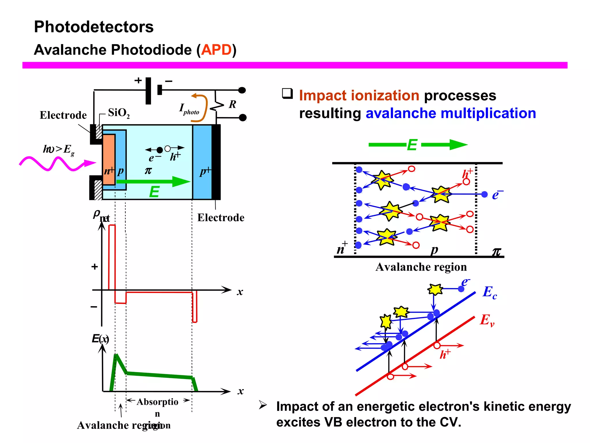
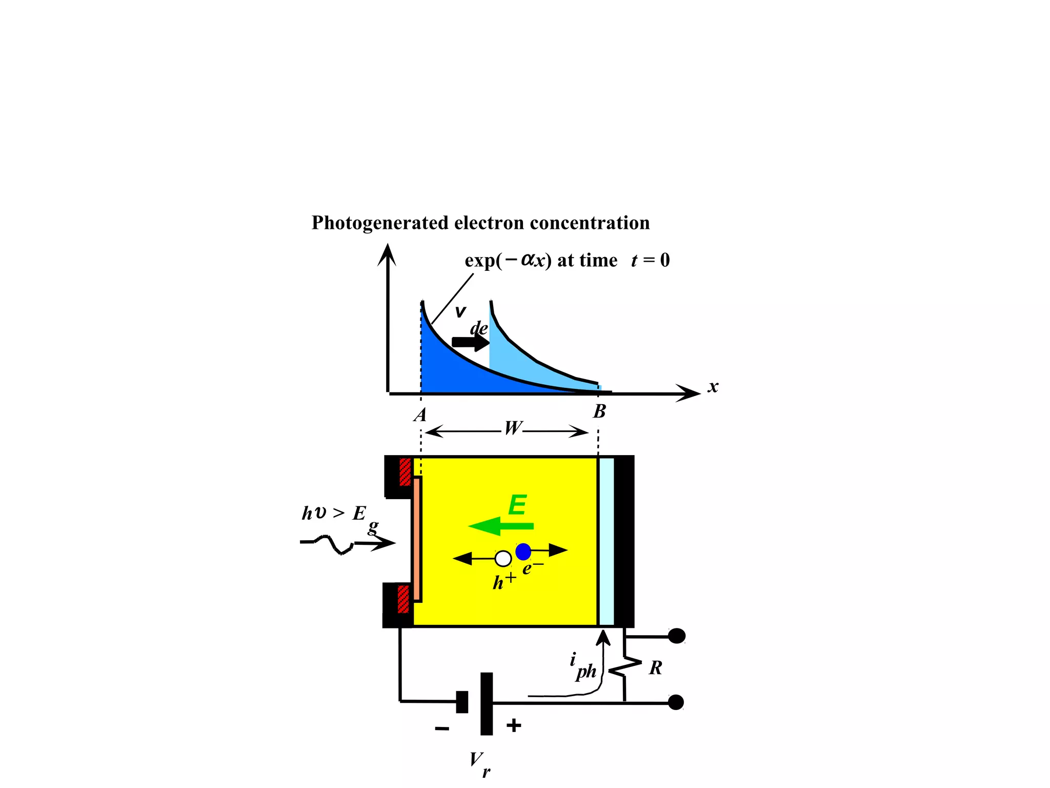

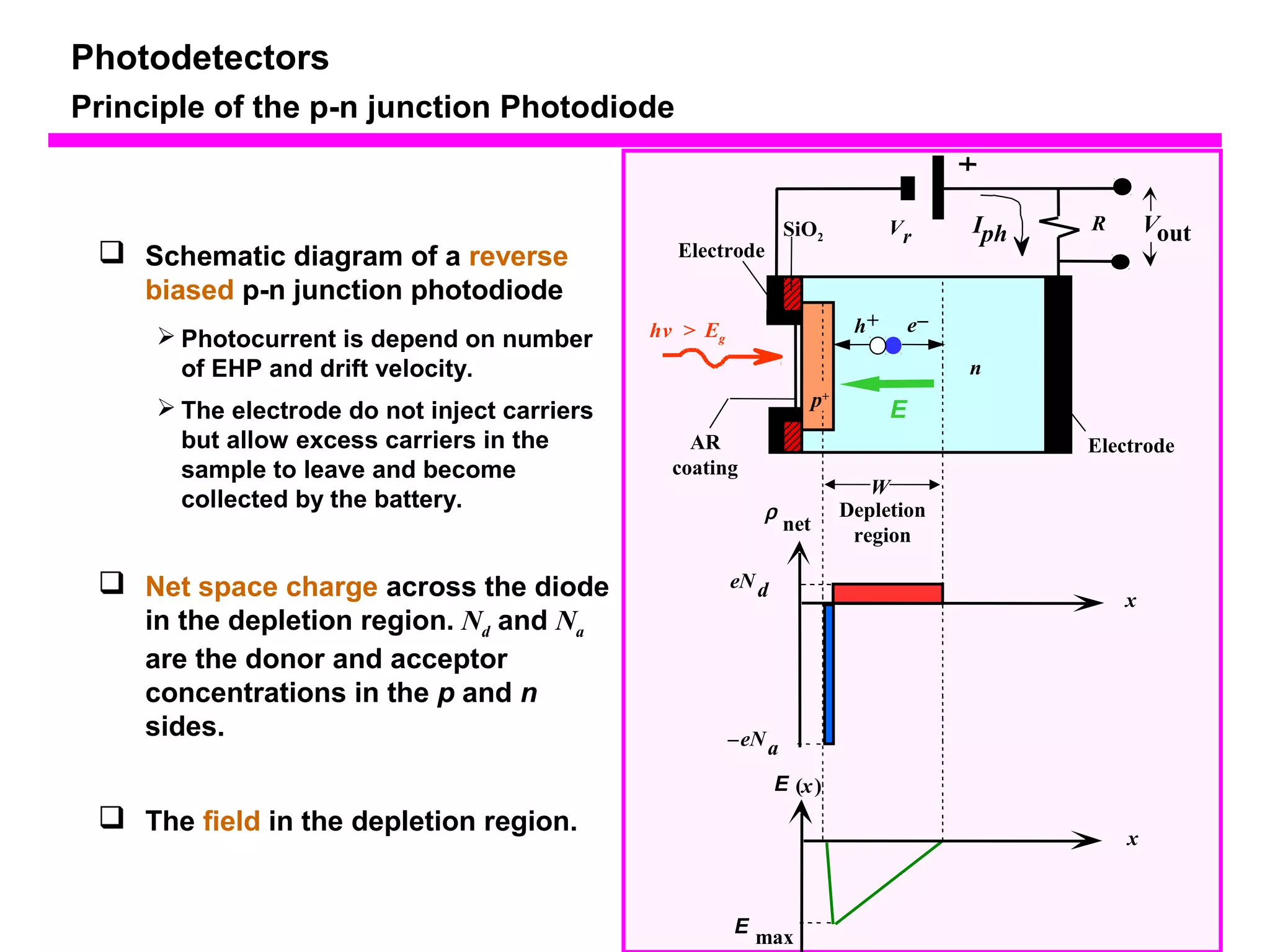
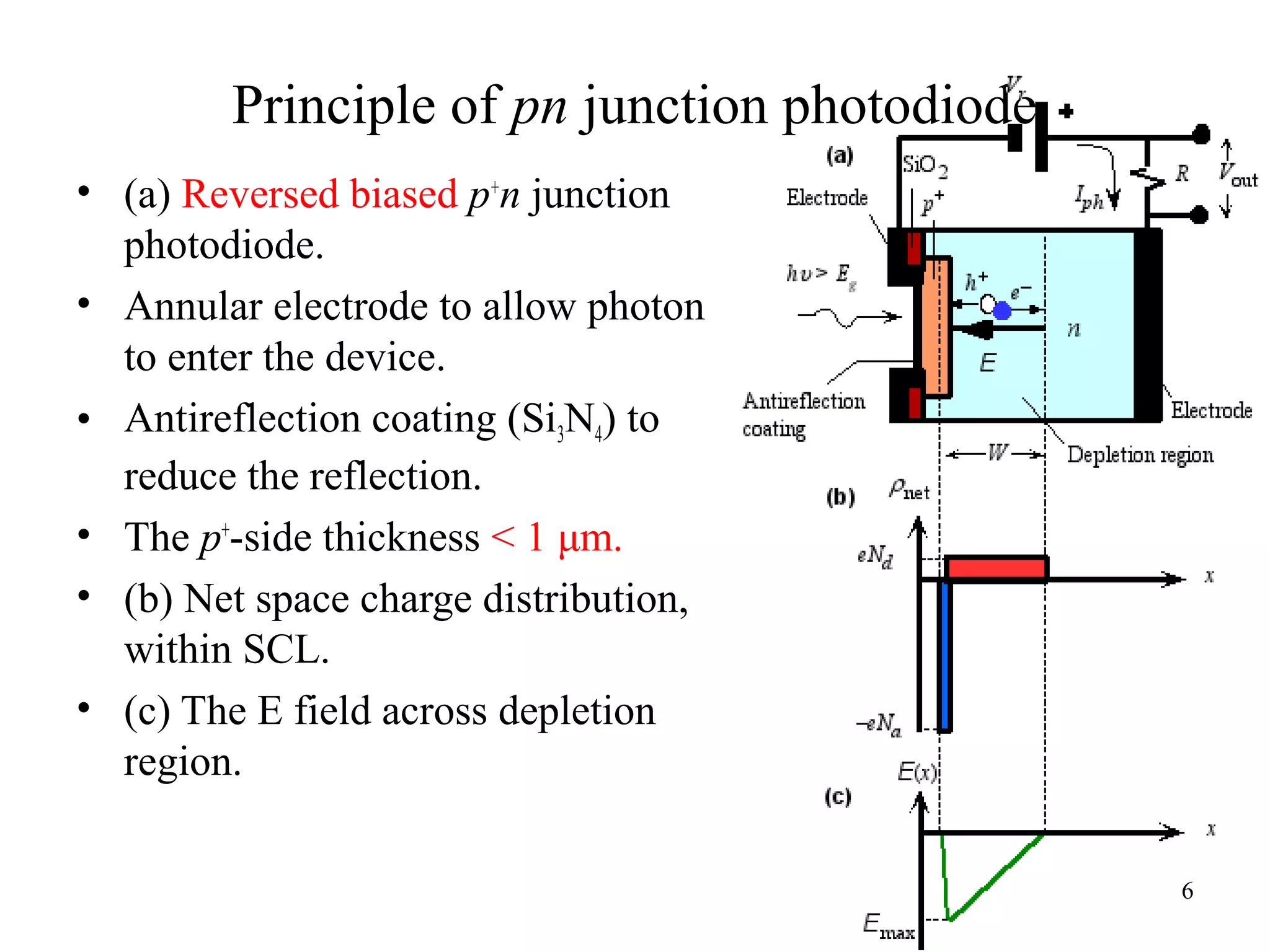
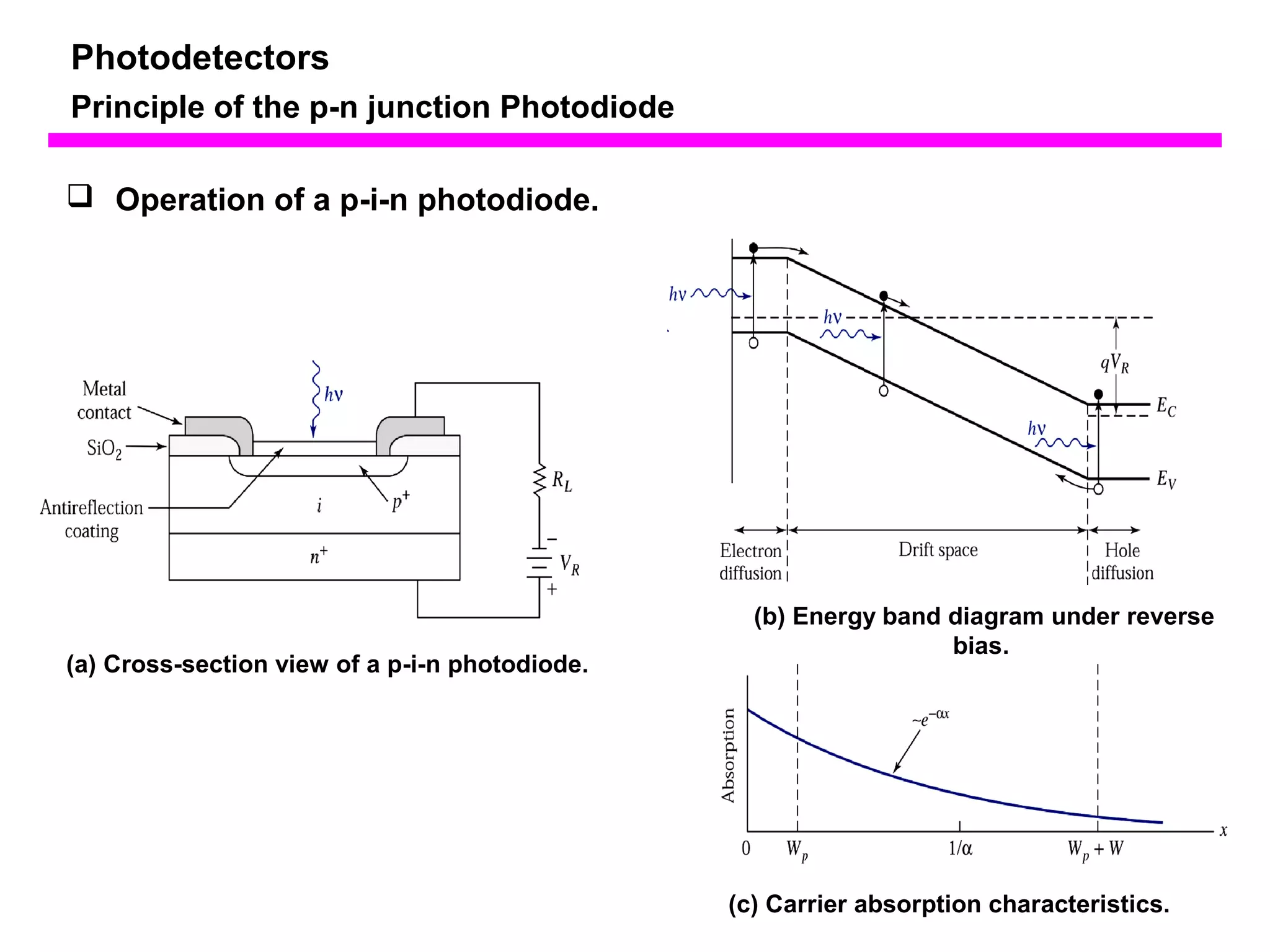
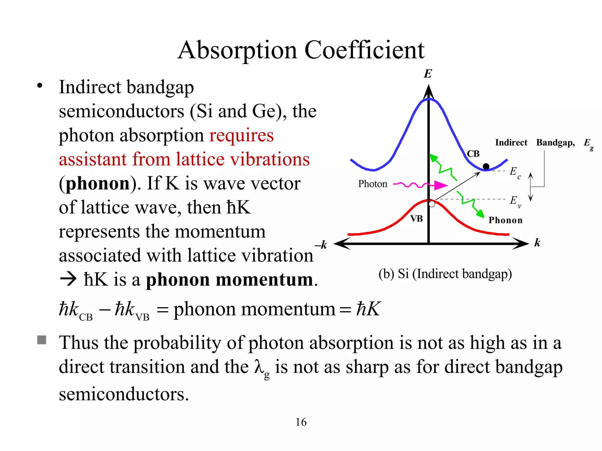
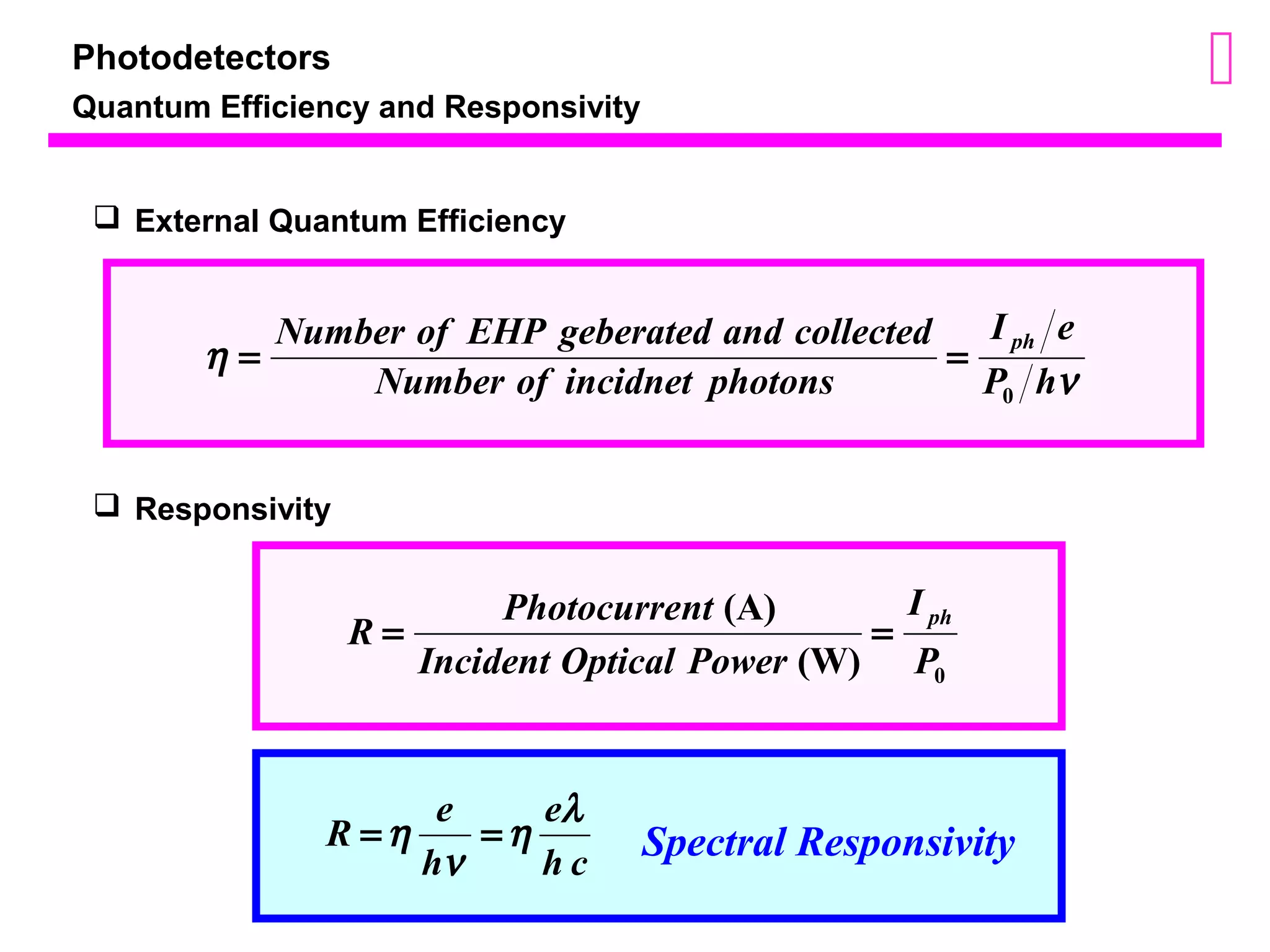
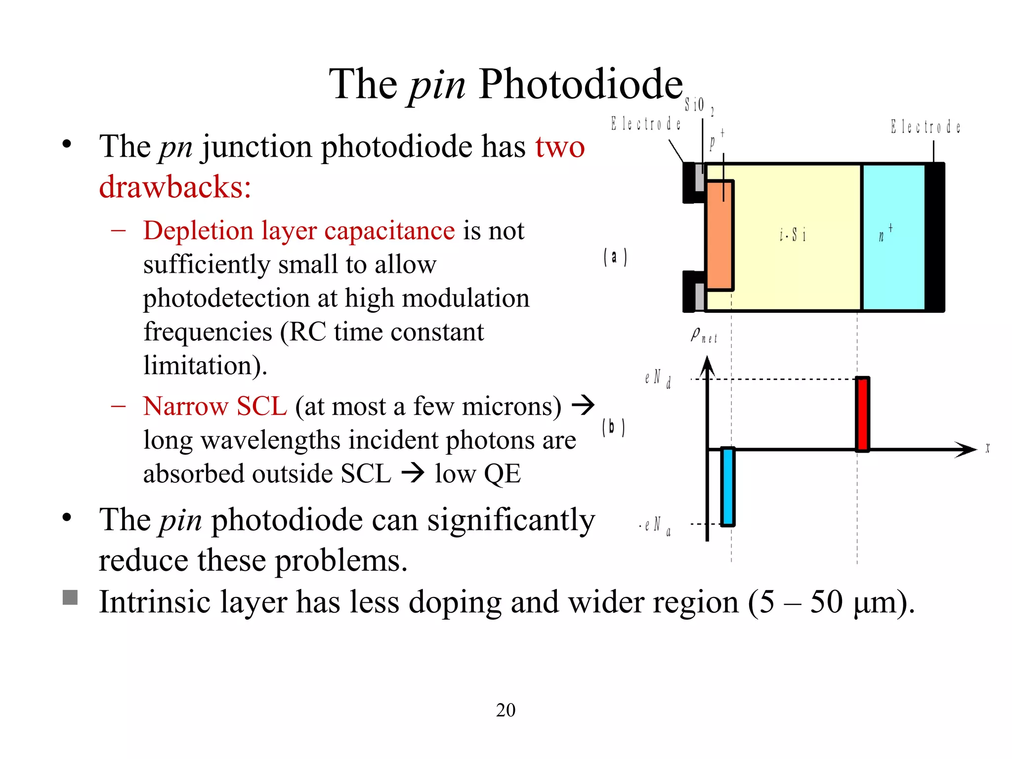
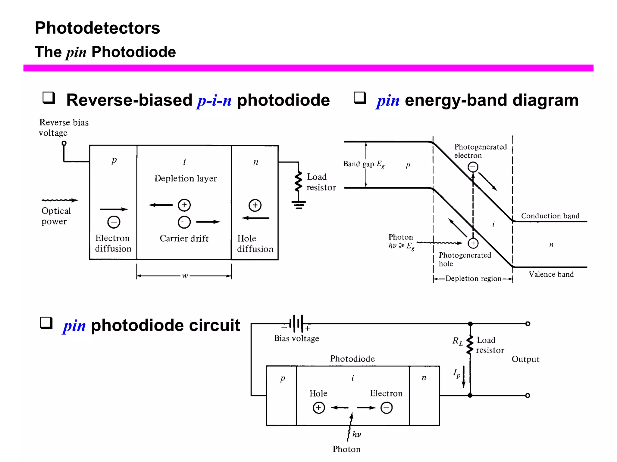
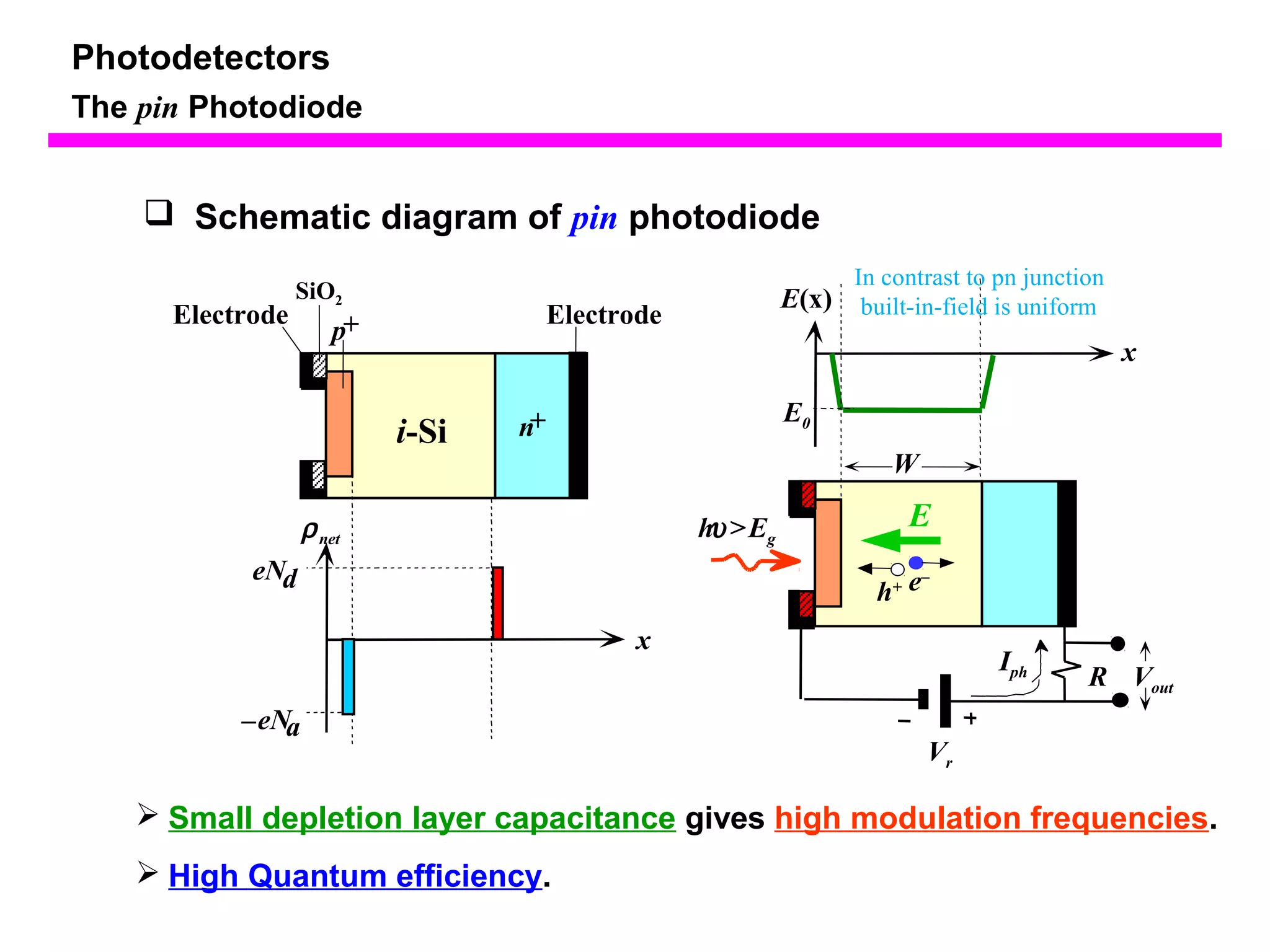
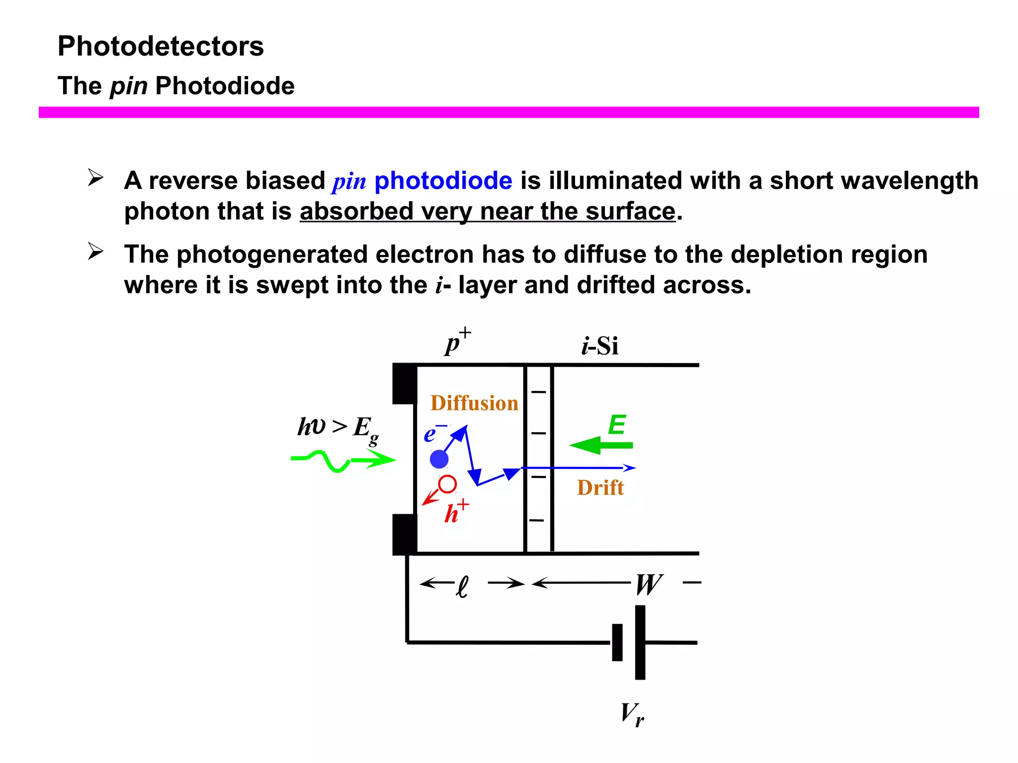
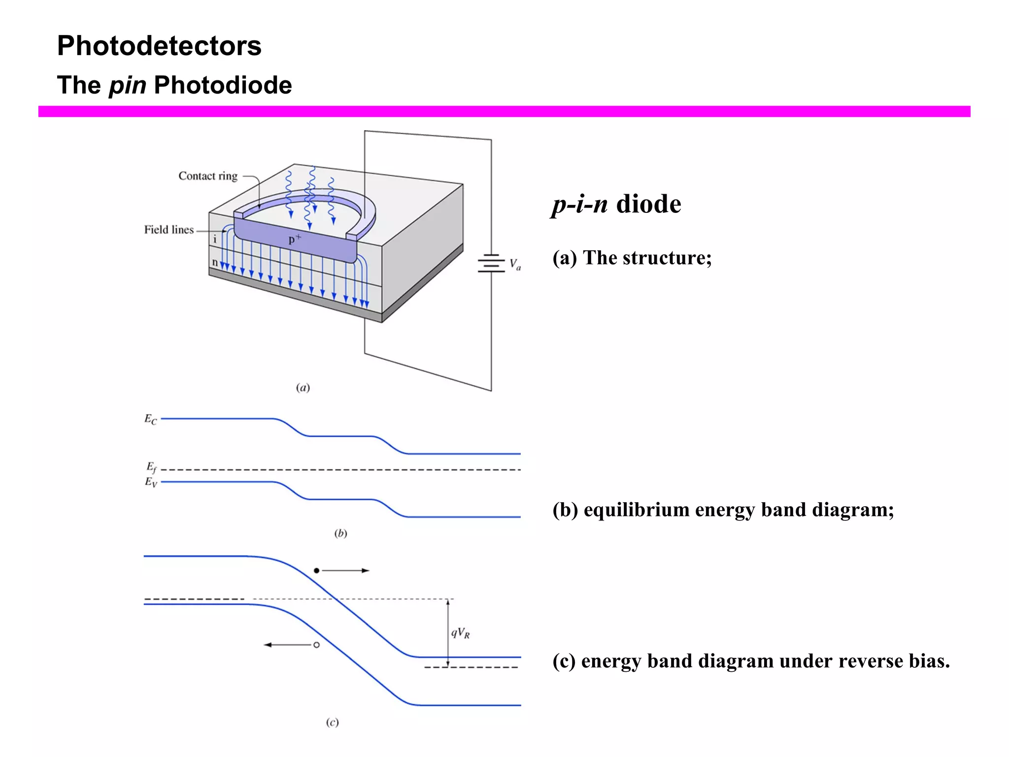
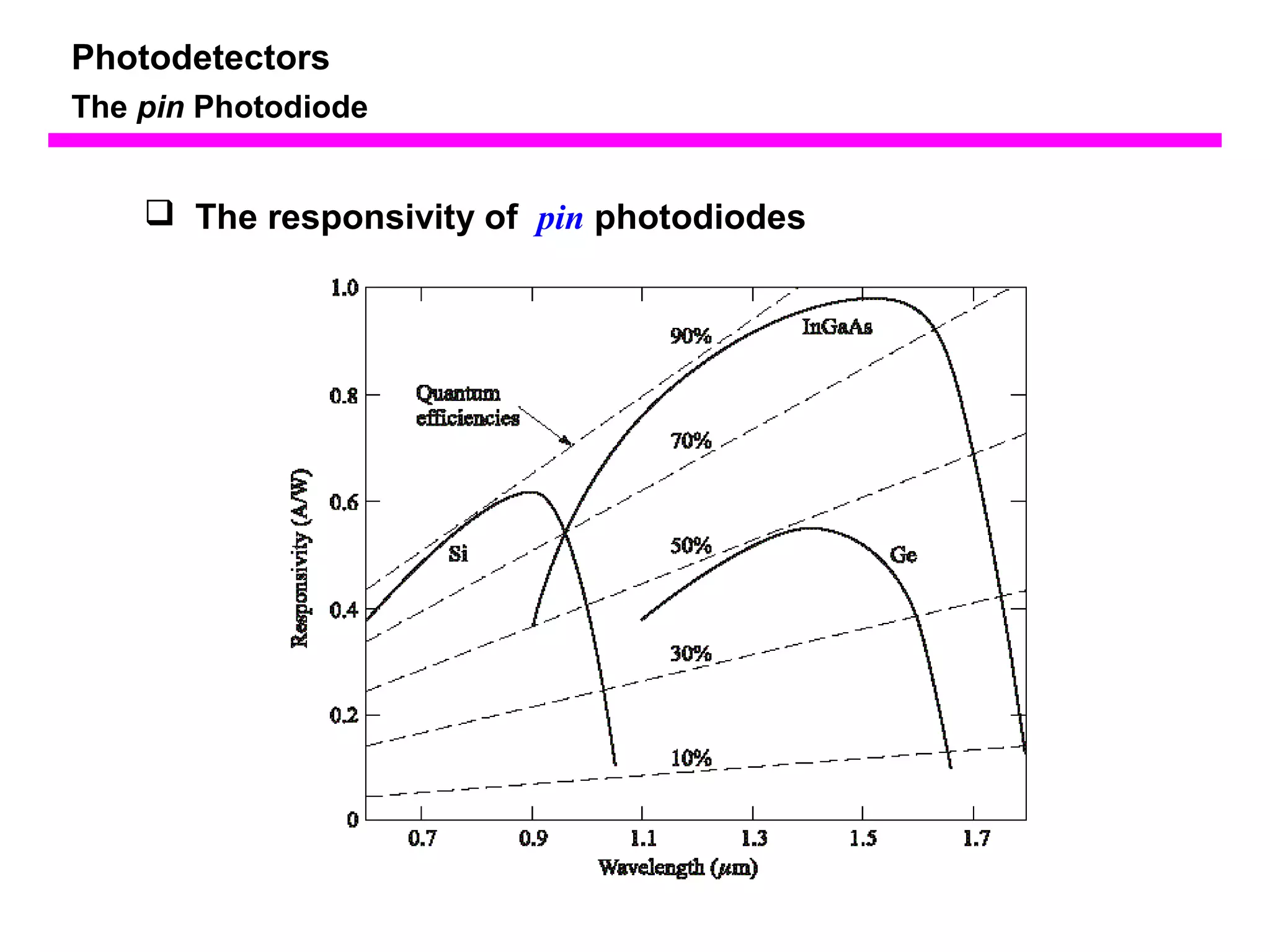
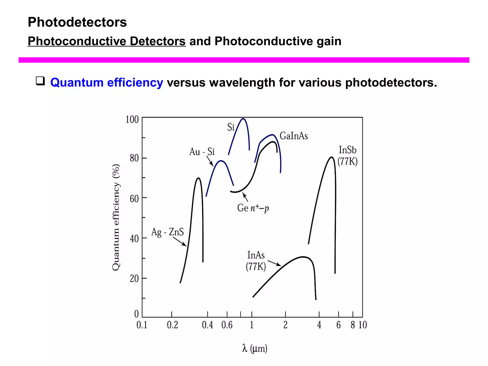
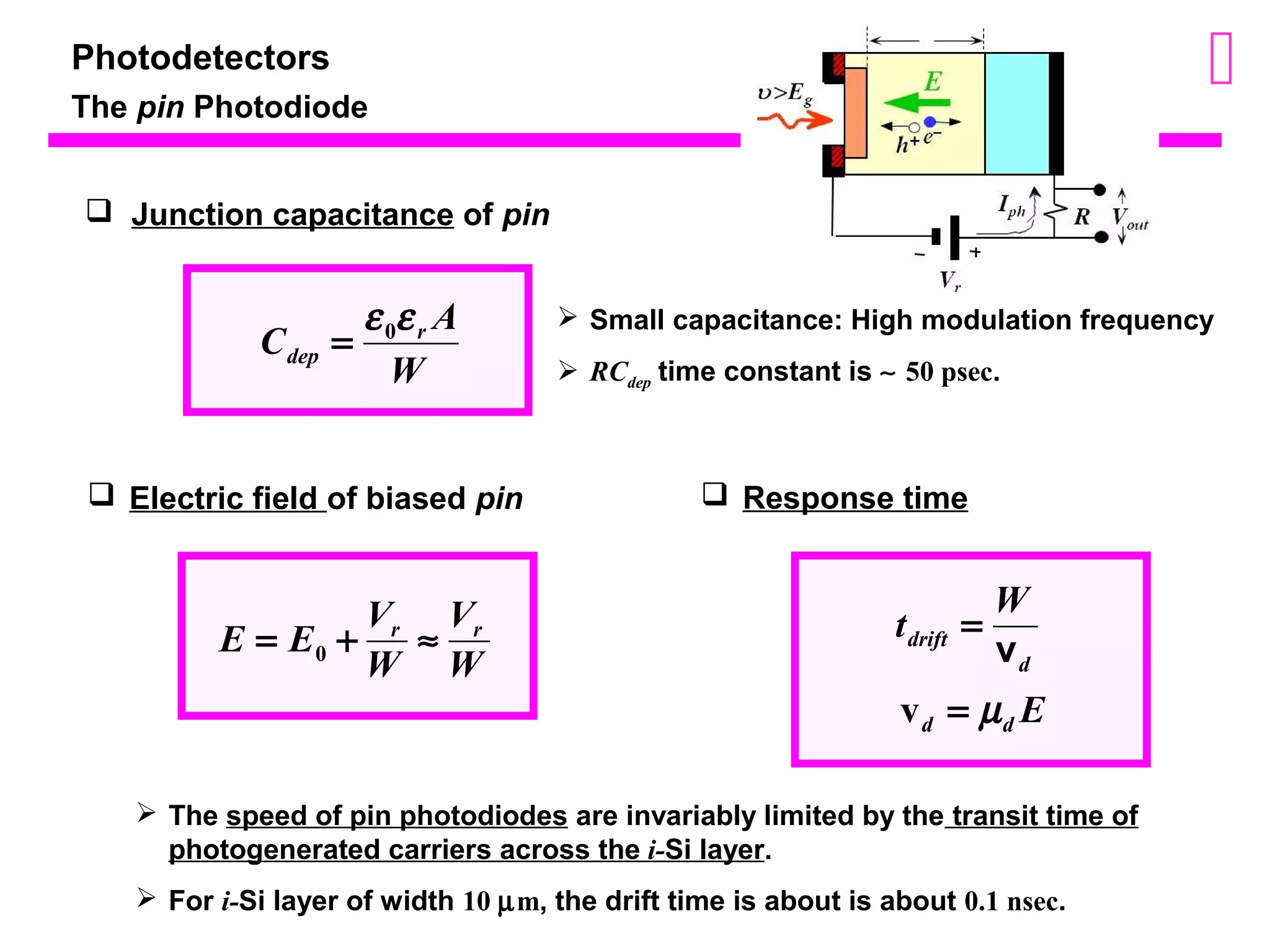
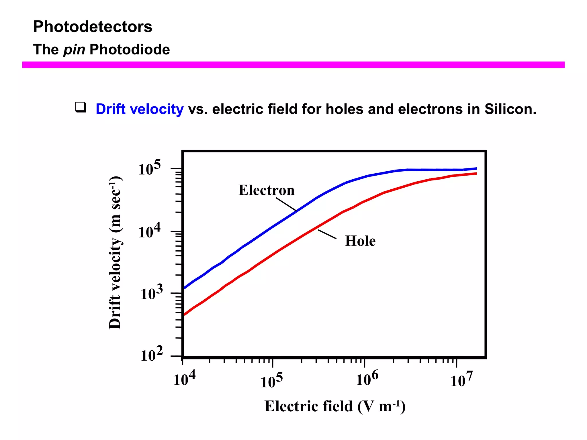
The document discusses photodetectors and the principles of p-n junction photodiodes. It describes the depletion region of a reverse biased p-n junction and how electron-hole pairs generated by photons are separated by the electric field. It also discusses pin photodiodes and how their intrinsic region allows for higher quantum efficiency and modulation frequencies compared to p-n junction photodiodes. Absorption coefficients of various semiconductor materials are shown as well as how direct and indirect bandgap materials differ in photon absorption.


![Coded Agents – with UiPath SDK + LangGraph [Virtual Hands-on Workshop]](https://cdn.slidesharecdn.com/ss_thumbnails/codedagentsdeck-251215155422-5497c599-thumbnail.jpg?width=640&height=640&fit=bounds)


