Download as PDF, PPTX
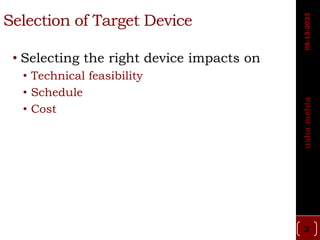
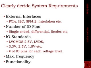
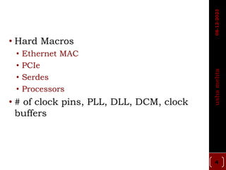
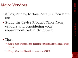
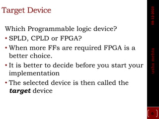
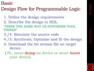
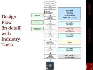
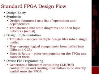
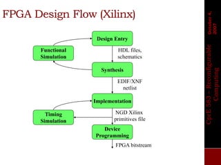
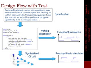
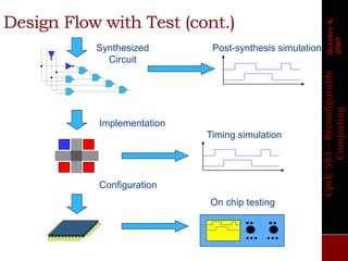


The document describes the basic design flow for FPGA development, including selecting a target device, defining system requirements, and major steps in the design process. Key aspects covered are selecting an FPGA with sufficient resources and I/O standards to meet requirements, defining functionality and interfaces in HDL code, simulating and synthesizing the design, and programming the FPGA with a generated bitstream file. Standard FPGA tools are used to implement the design through synthesis, mapping, placement and routing steps.


![[Deck] What's New in Spark-Iceberg Integration via DSV2.pptx](https://cdn.slidesharecdn.com/ss_thumbnails/deckwhatsnewinspark-icebergintegrationviadsv2-260210005337-25955b12-thumbnail.jpg?width=640&height=640&fit=bounds)


