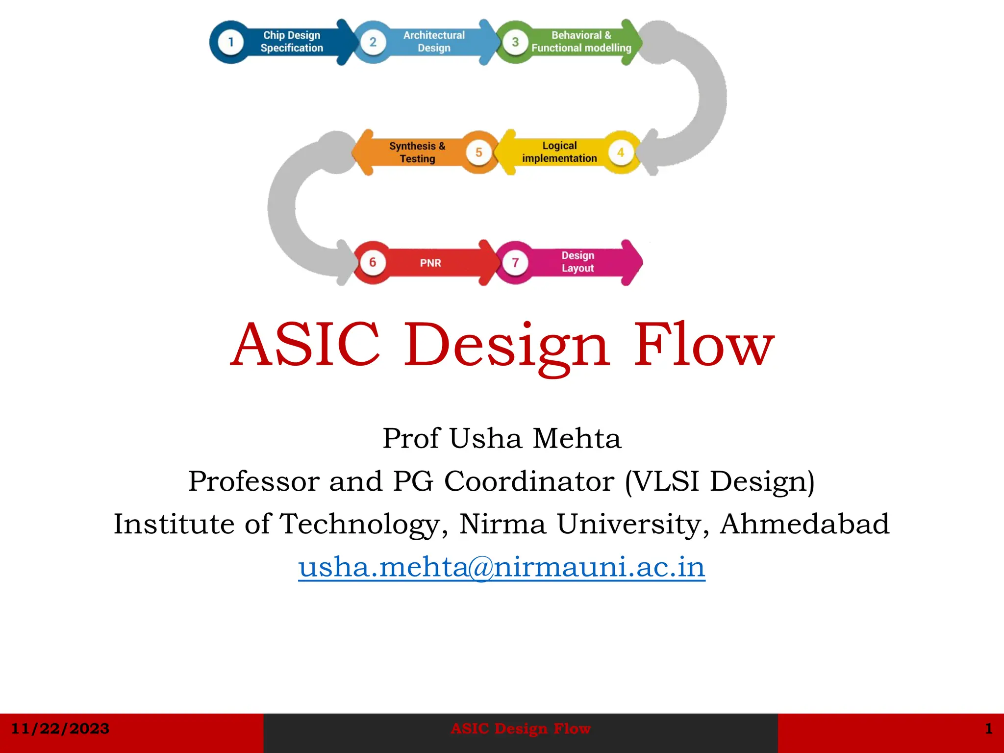

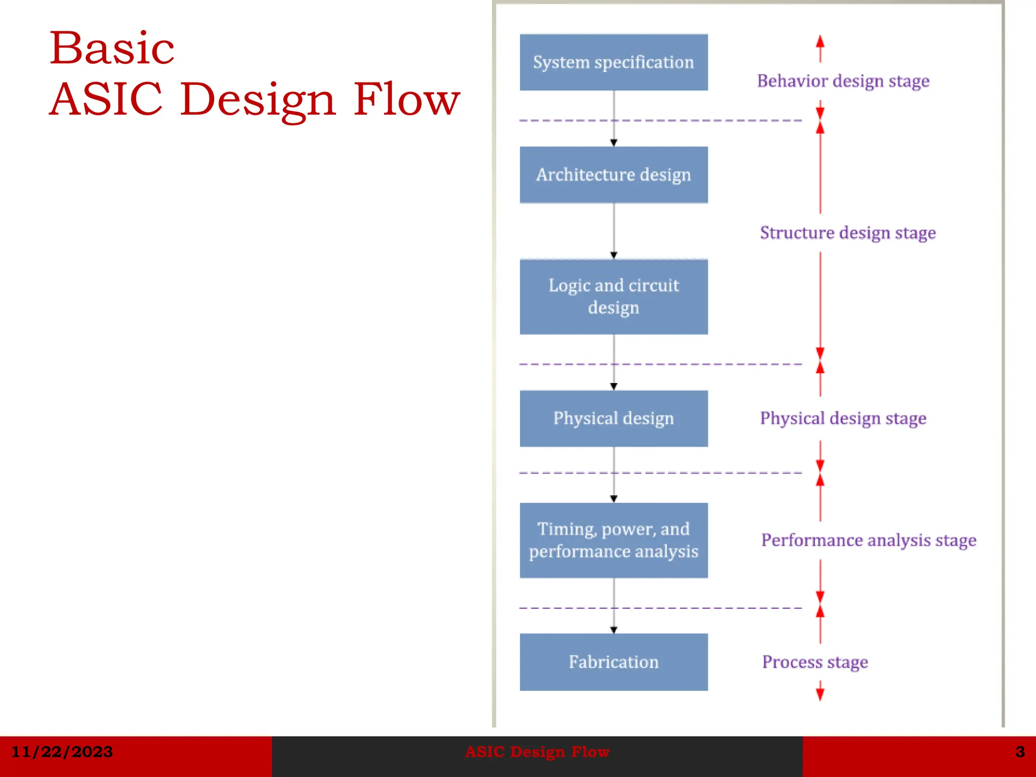
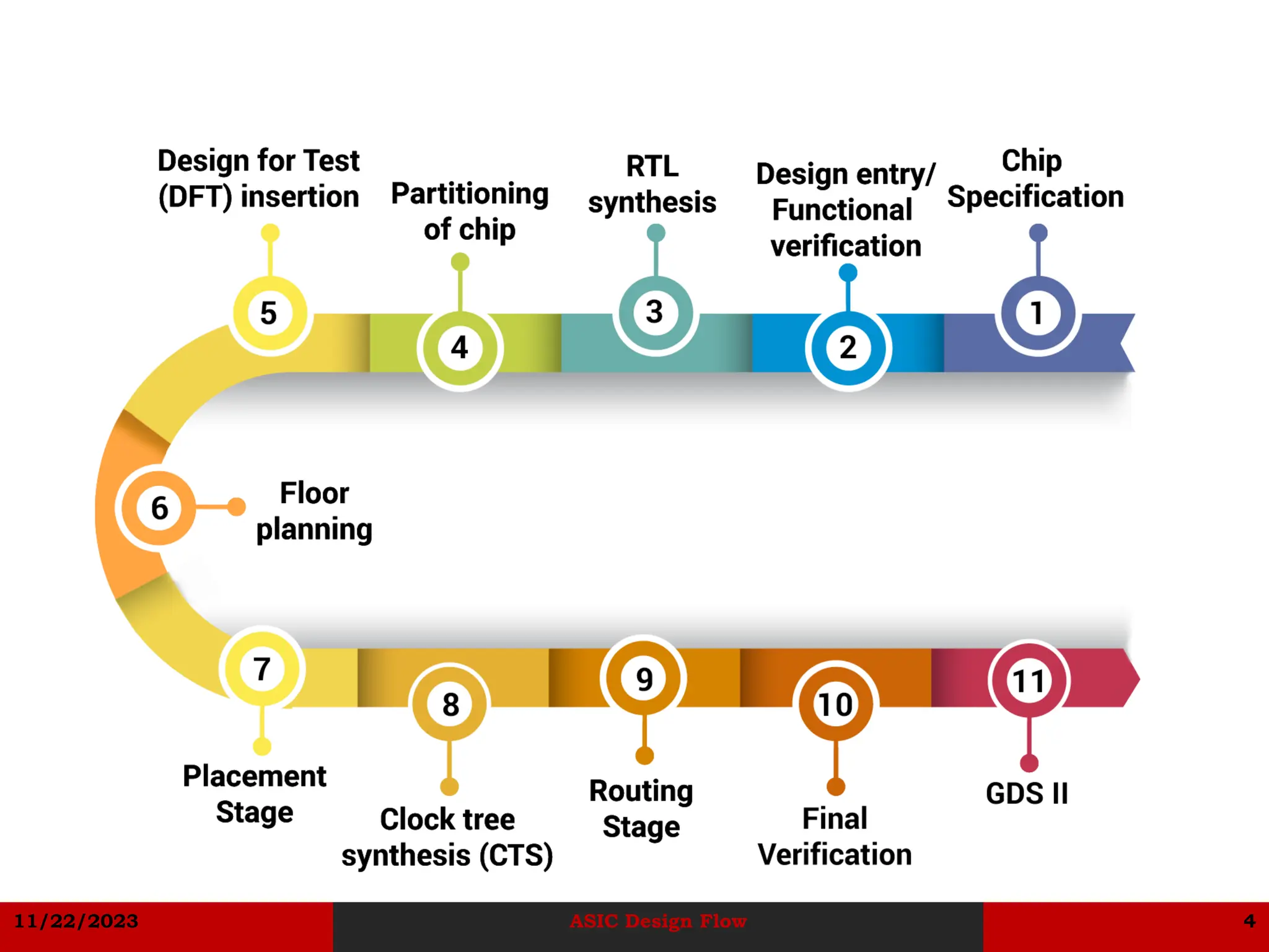
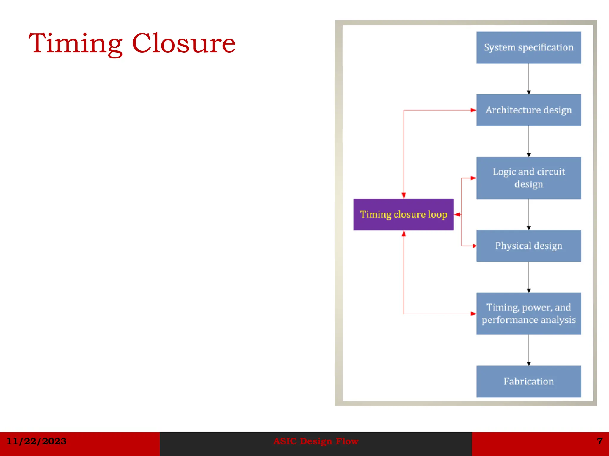
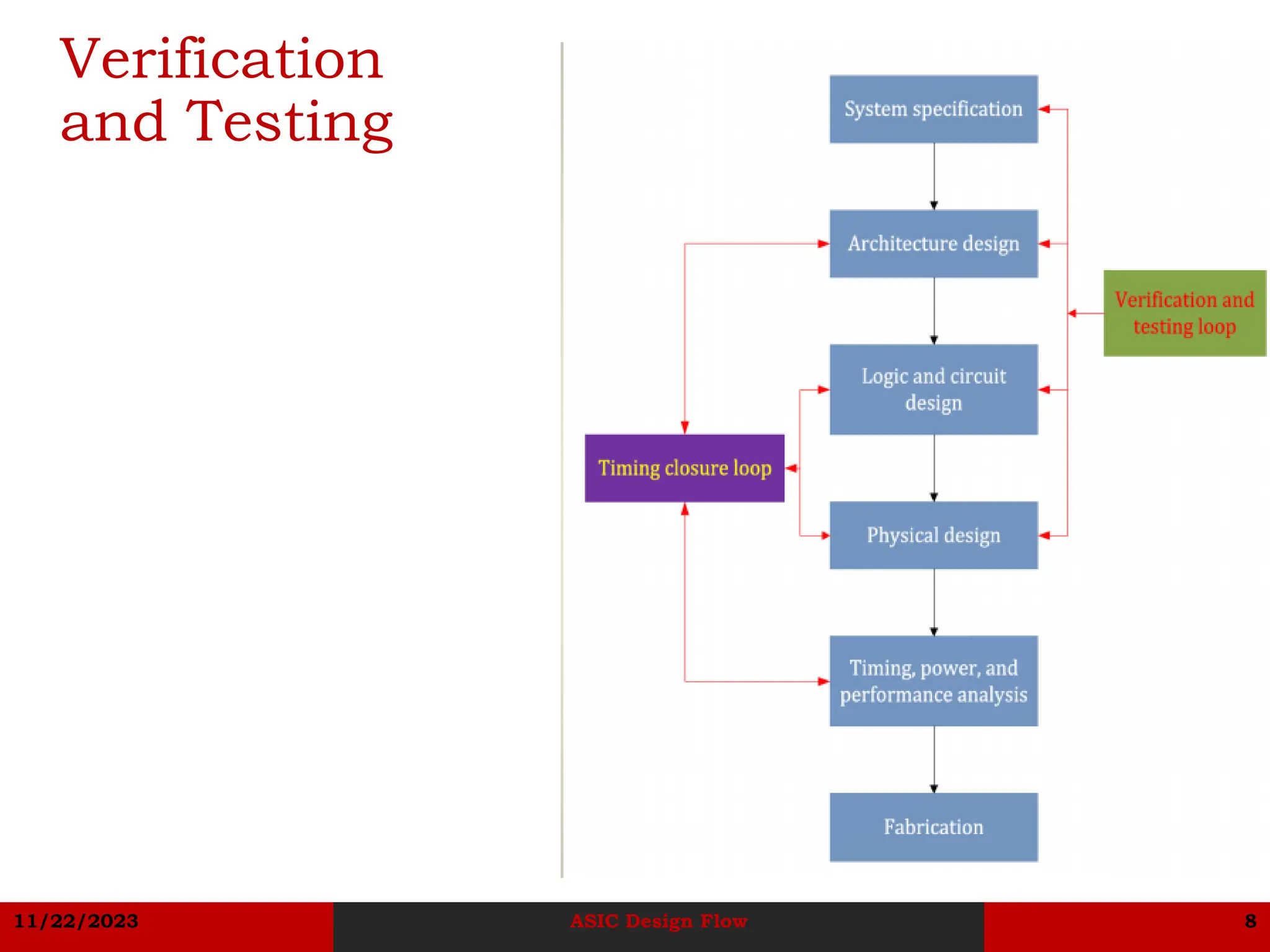
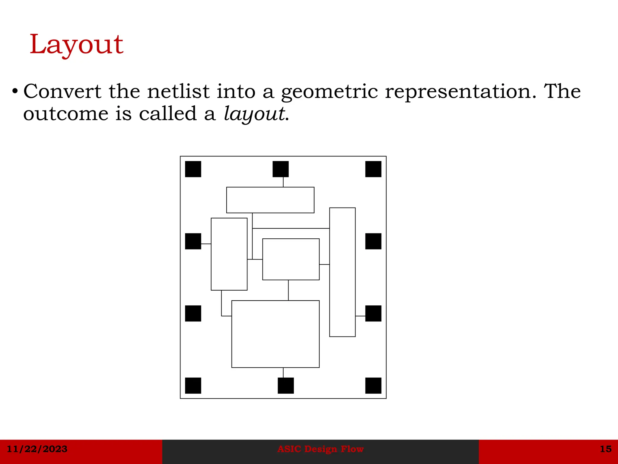
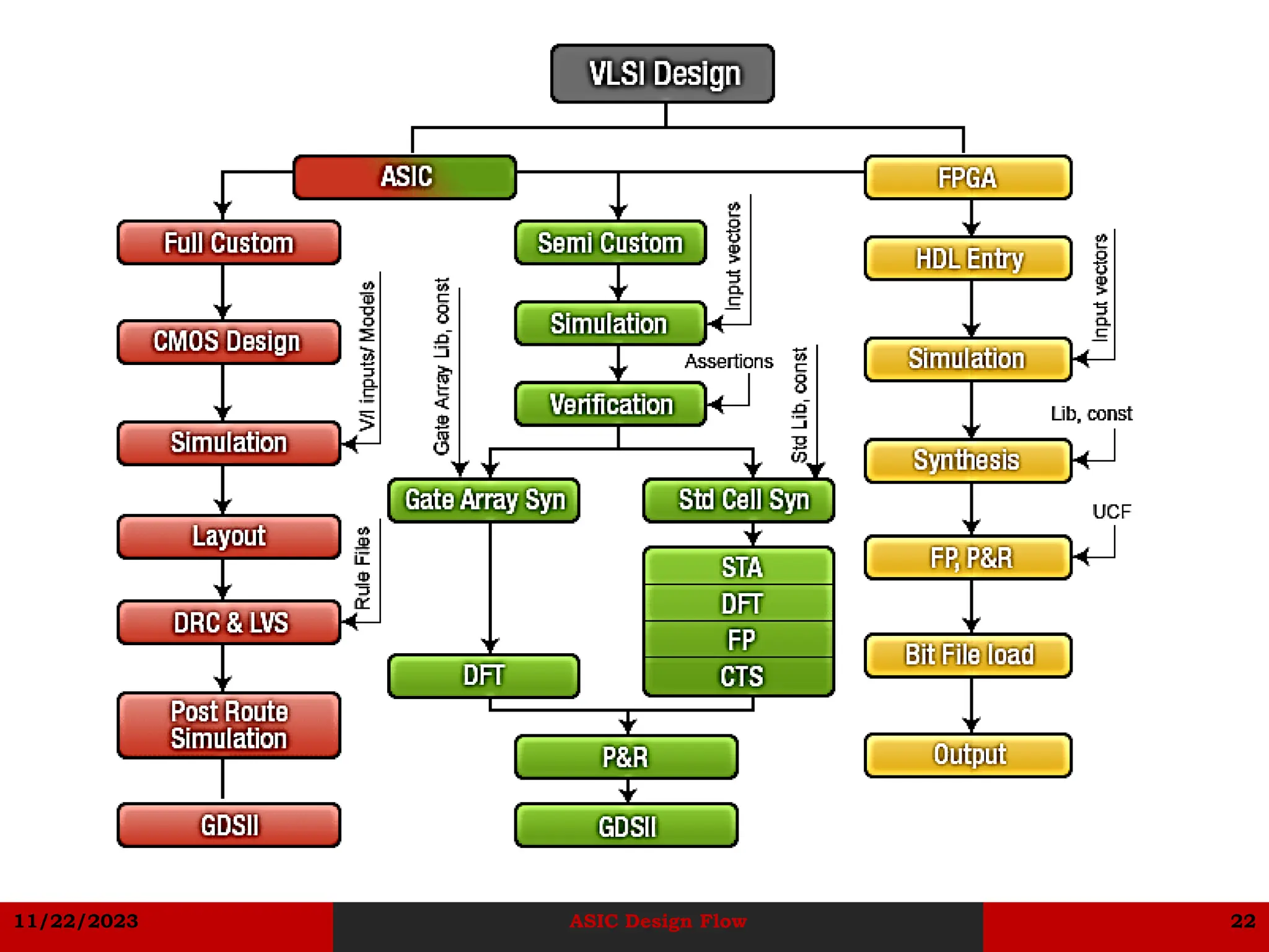
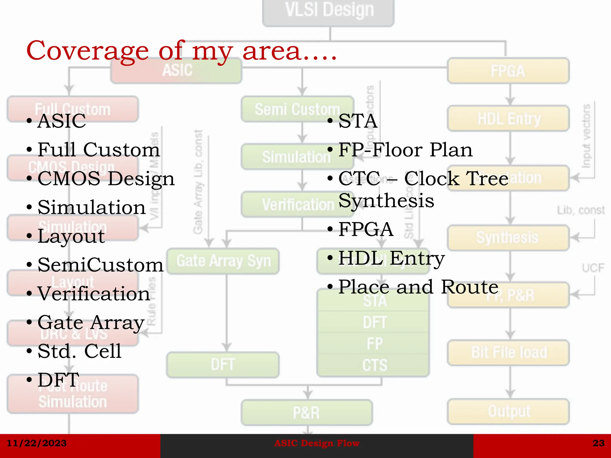

The document describes the basic ASIC design flow. It begins with system specification and proceeds through architectural design, functional design, register transfer level design, logic design, circuit design, layout, and verification and testing. However, the document notes that the design flow is not strictly linear and there can be interactions between stages that require going back to earlier stages. Timing closure is identified as resolving any timing issues that arise through iterations between physical design and earlier stages.