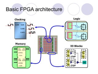
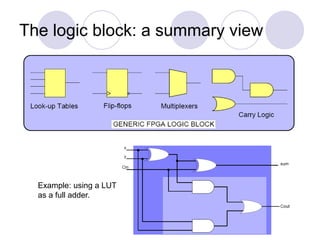
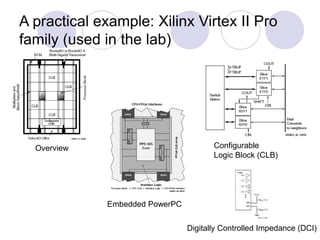
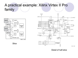
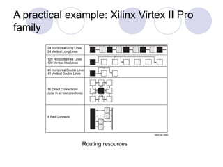
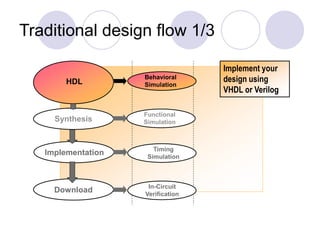
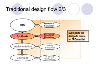
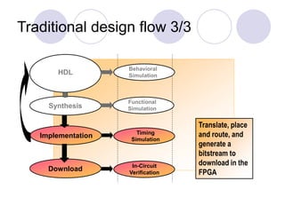
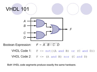
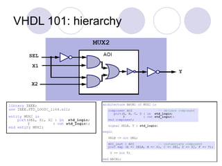
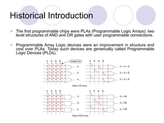
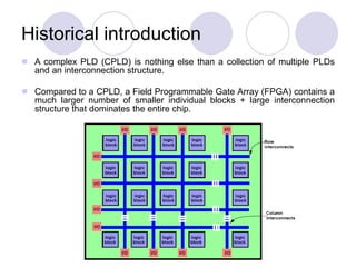
This document provides a summary of an introduction to field programmable gate arrays (FPGAs) lecture. It begins with a brief history of digital design and programmable logic, including how FPGAs evolved from programmable logic arrays and complex programmable logic devices. It then covers basics of digital design principles like synchronous design and combinational vs sequential logic. The document outlines FPGA architecture including logic blocks, routing resources, and examples from Xilinx Virtex II Pro family. It also summarizes the traditional FPGA design flow and highlights of VHDL and concludes with an overview of the demo portion of the lecture.
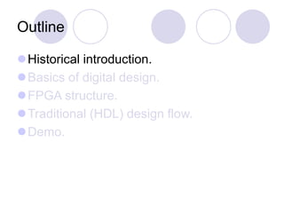

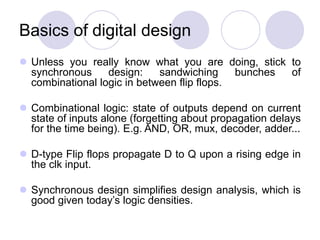
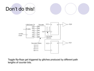
![Basics of (synchronous) Digital Design
dataSelectC
dataAC[31:0]
dataBC[31:0]
dataSelectCD1
dataACd1[31:0]
DataOut_3[31:0]
0
1
DataOut[31:0]
sum_1[31:0]
+
sum[31:0]
DataOut[31:0]
[31:0]
DataInB[31:0] [31:0]
DataInA[31:0] [31:0]
DataSelect
Clk
Q[0]
D[0]
[31:0]
Q[31:0]
[31:0]
D[31:0]
[31:0]
Q[31:0]
[31:0]
D[31:0]
Q[0]
D[0]
[31:0]
Q[31:0]
[31:0]
D[31:0] [31:0]
[31:0]
[31:0] [31:0]
Q[31:0]
[31:0]
D[31:0]
[31:0]
[31:0]
[31:0] [31:0]
Q[31:0]
[31:0]
D[31:0]
High clock rate:
144.9 MHz on a
Xilinx Spartan IIE.
Higher clock rate:
151.5 MHz on the
same chip.
dataSelectC
dataAC[31:0]
dataBC[31:0]
sum[31:0]
+
DataOut_3[31:0]
0
1
DataOut[31:0]
DataOut[31:0]
[31:0]
DataInB[31:0] [31:0]
DataInA[31:0] [31:0]
DataSelect
Clk
Q[0]
D[0]
[31:0]
Q[31:0]
[31:0]
D[31:0]
[31:0]
Q[31:0]
[31:0]
D[31:0]
[31:0]
[31:0]
[31:0]
[31:0]
[31:0]
[31:0] [31:0]
Q[31:0]
[31:0]
D[31:0]
6.90 ns
6.60 ns
Illustrating the latency/throughput tradeoff](https://image.slidesharecdn.com/anintroductiontofpga-240205191728-625985ce/85/An-Introduction-to-Field-Programmable-Gate-Arrays-10-320.jpg)