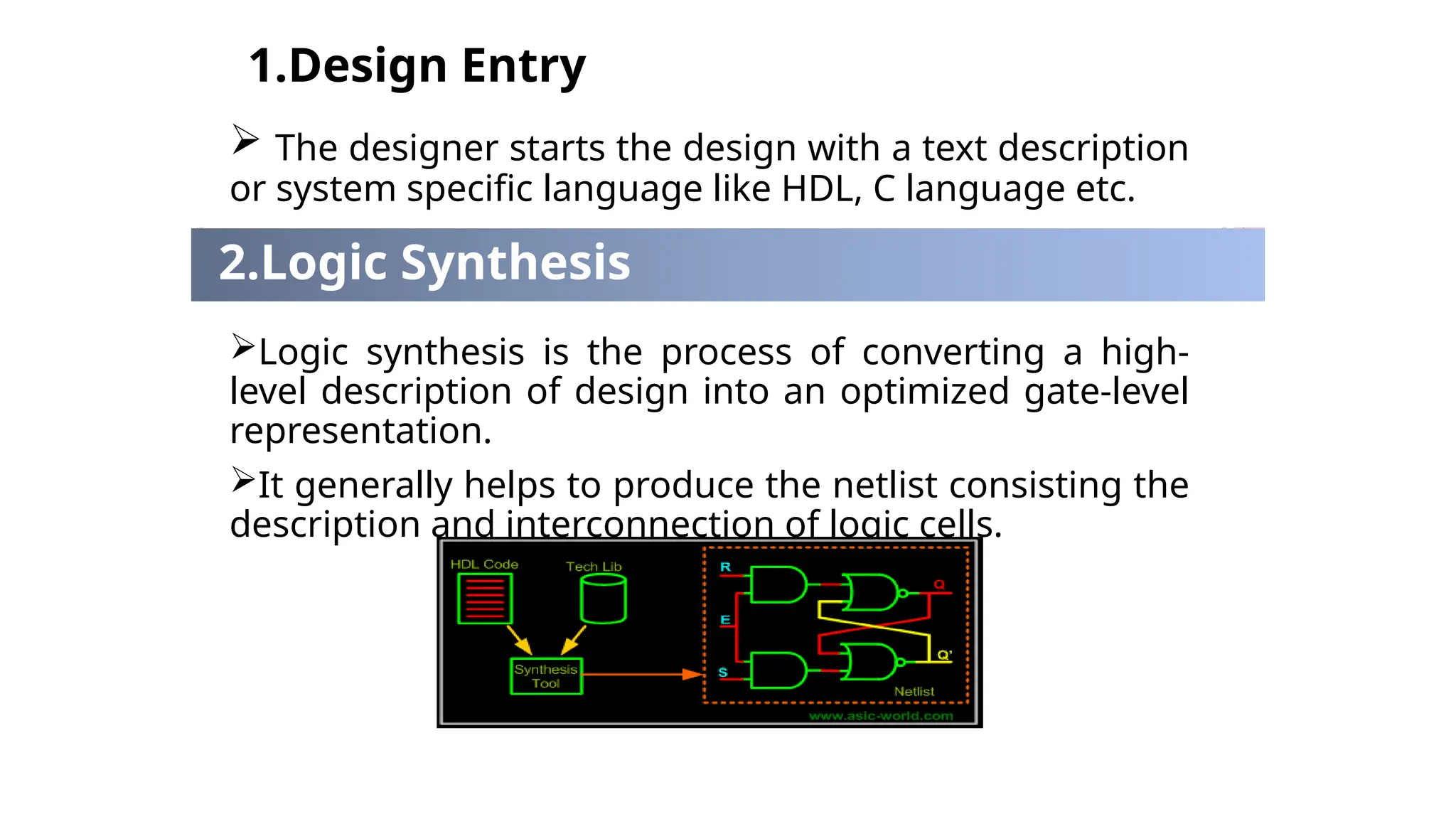
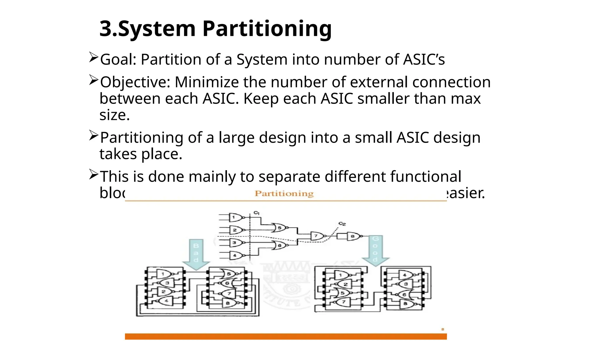
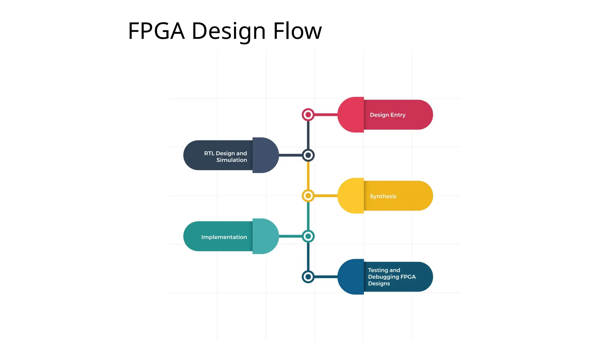
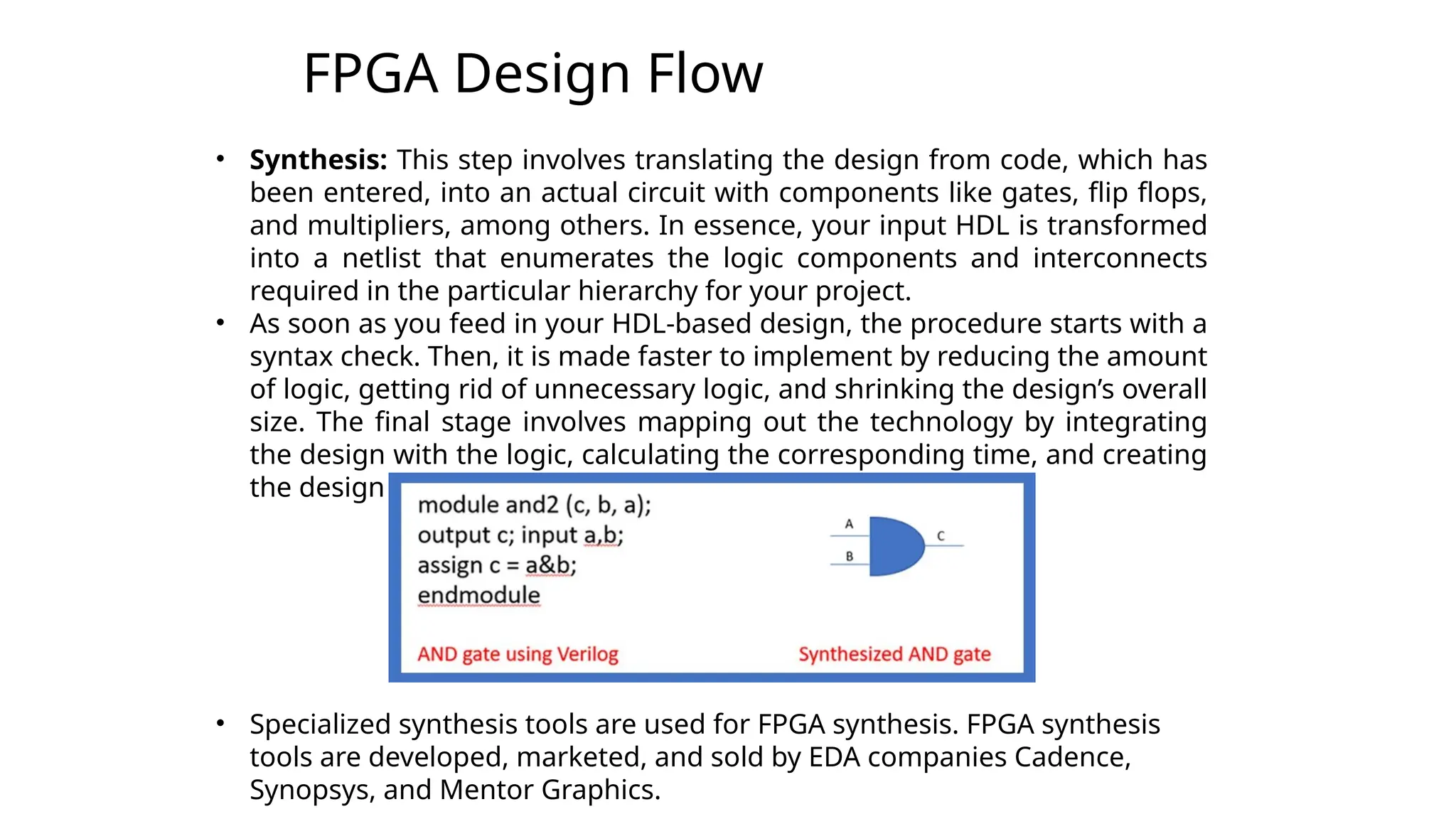
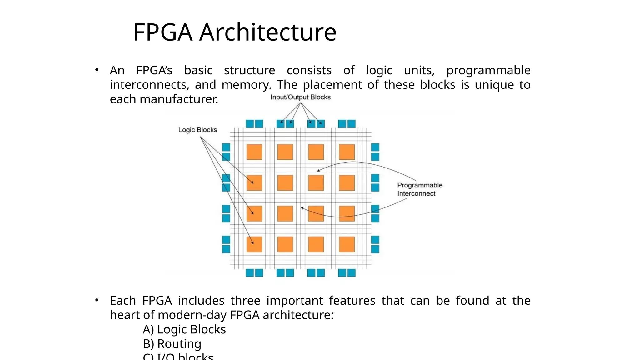
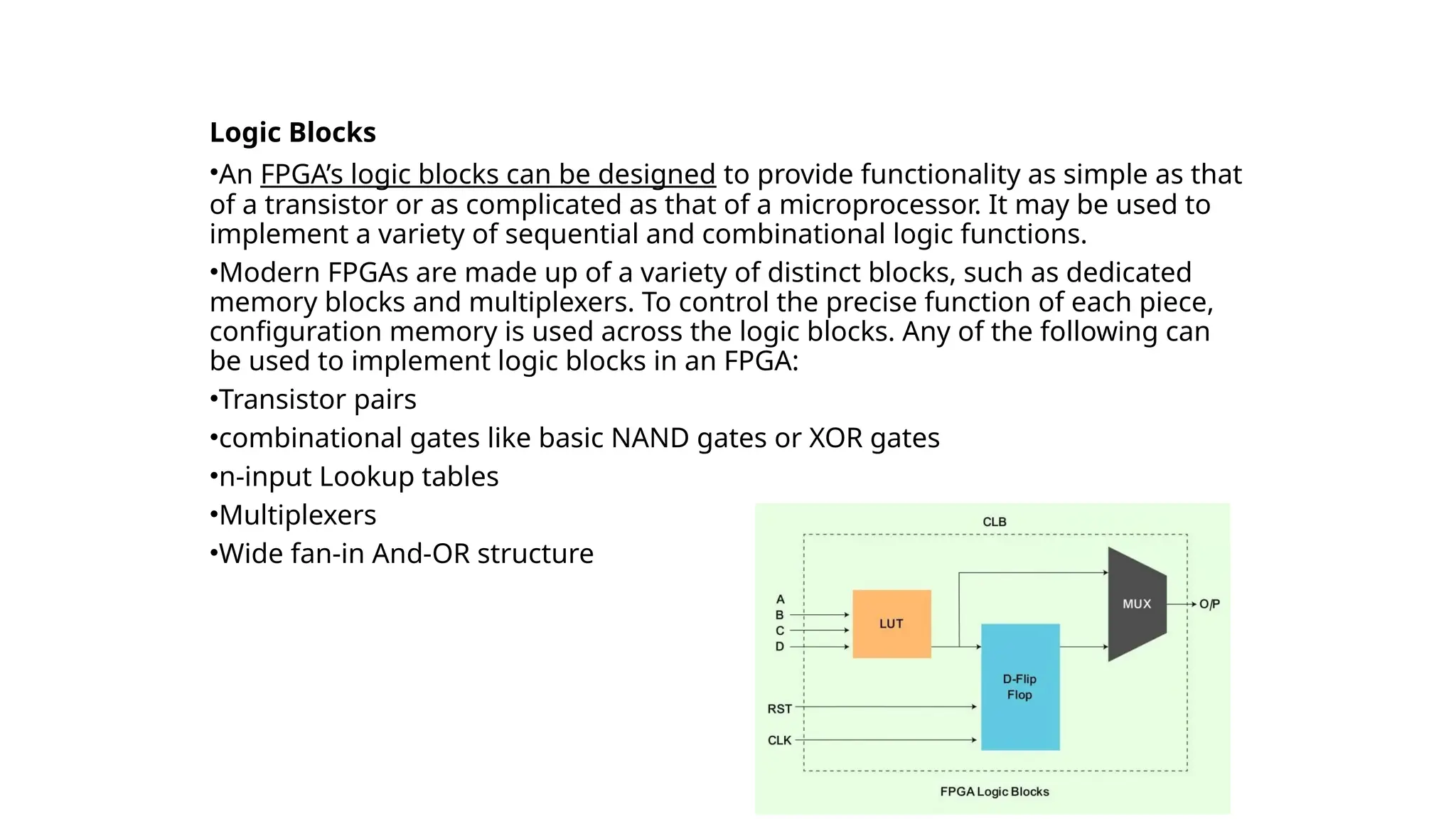
The document outlines the ASIC and FPGA design flows, detailing the steps involved from design entry to post-layout simulation for ASICs and from design entry to implementation for FPGAs. It describes various stages including logic synthesis, system partitioning, floorplanning, and routing, as well as the architecture of FPGAs consisting of logic units and programmable interconnects. Additionally, it highlights the significance of proper simulation and implementation tools in ensuring design accuracy and efficiency.