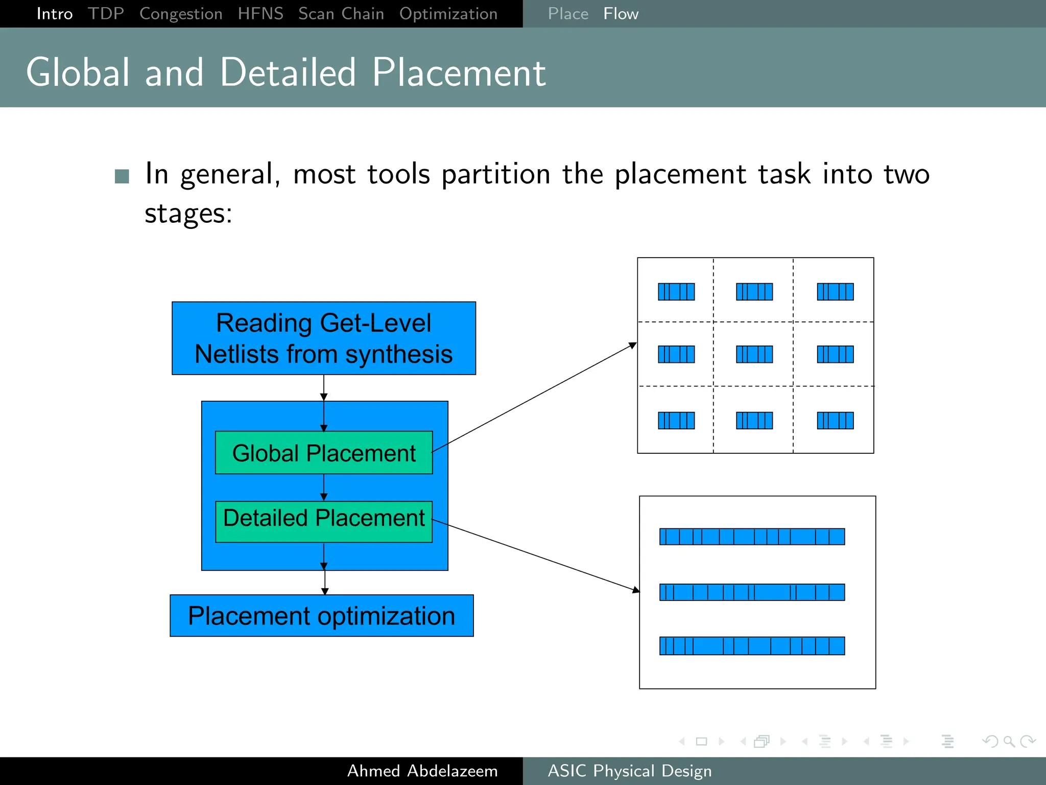
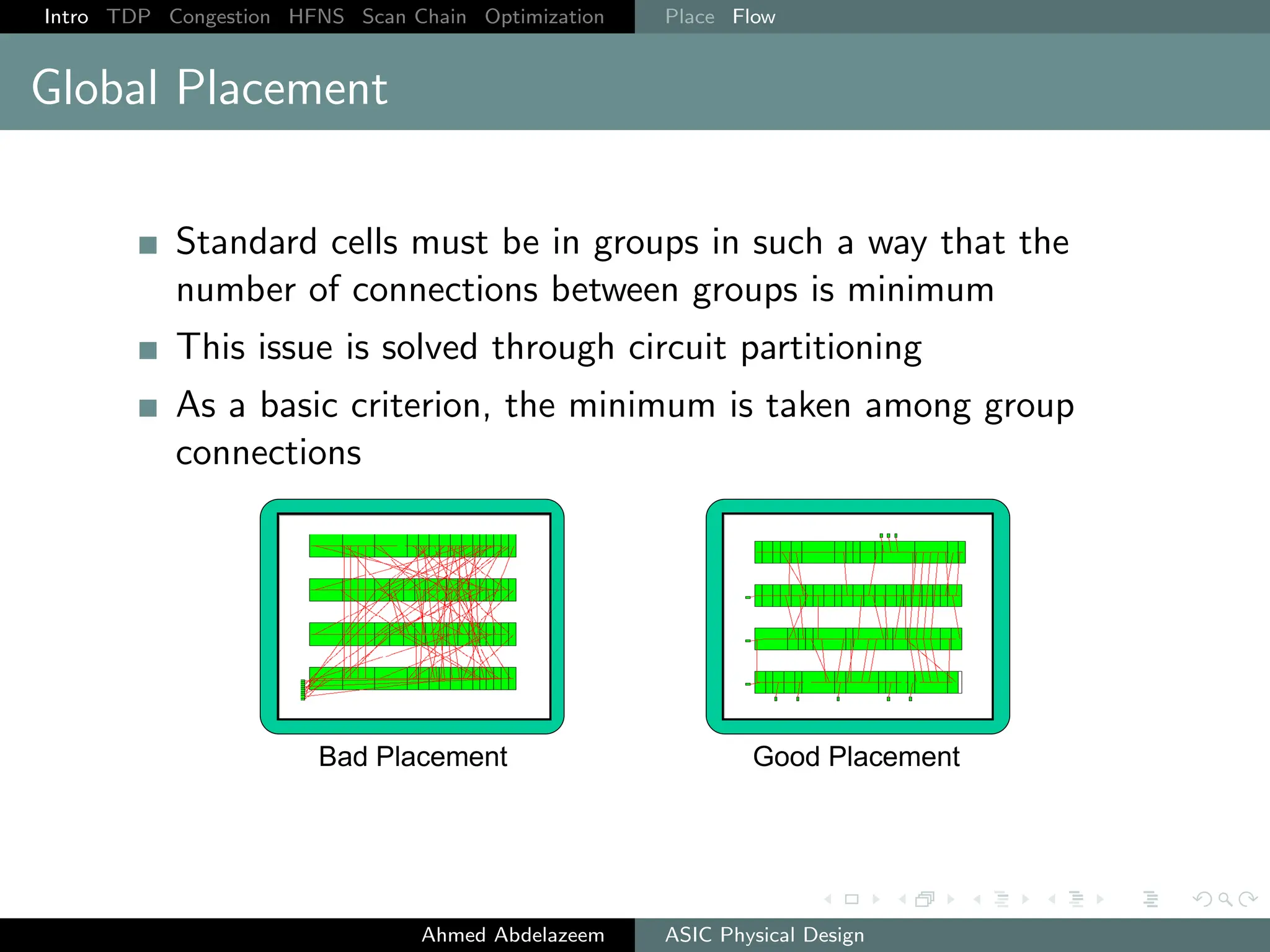
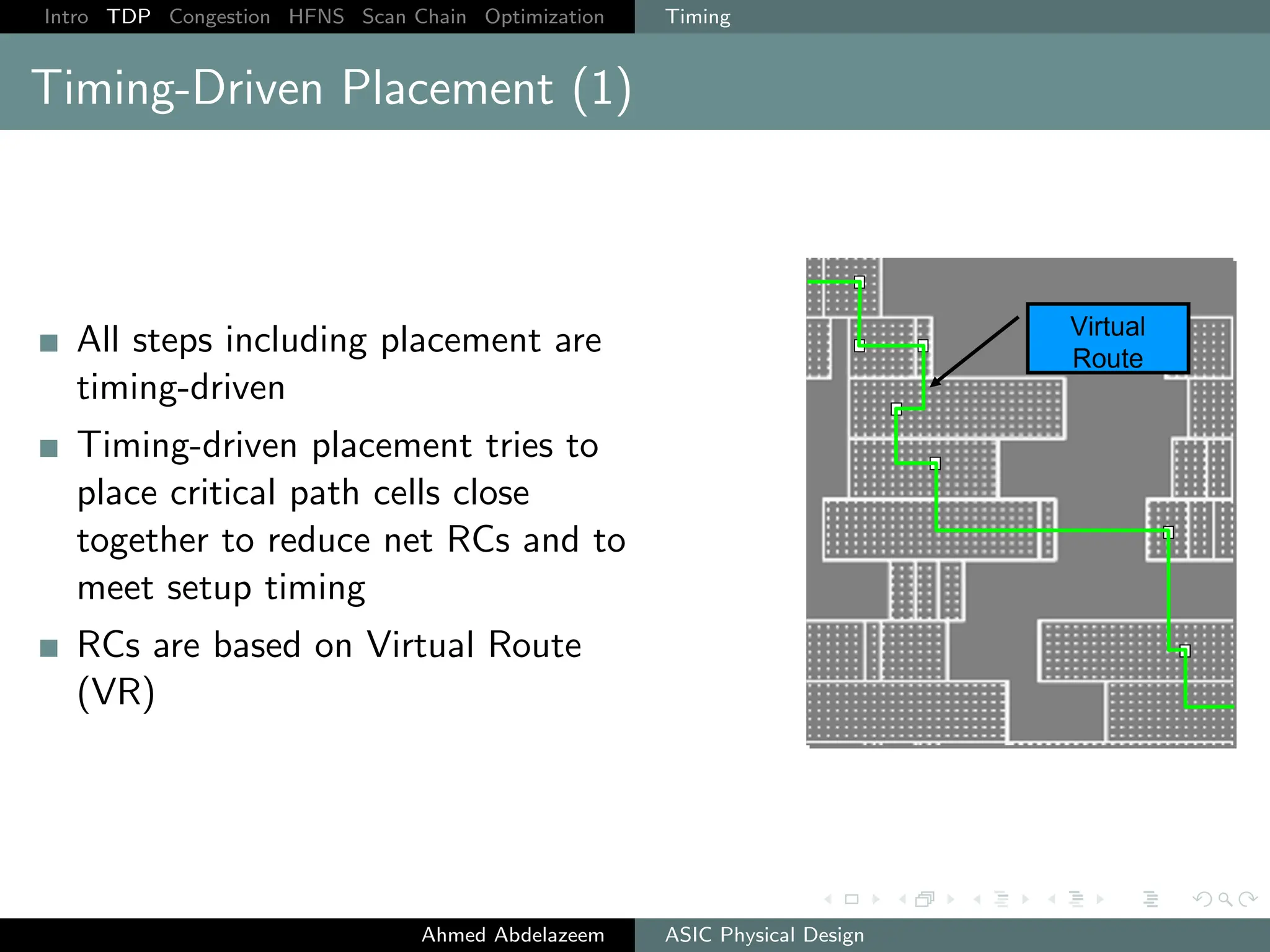
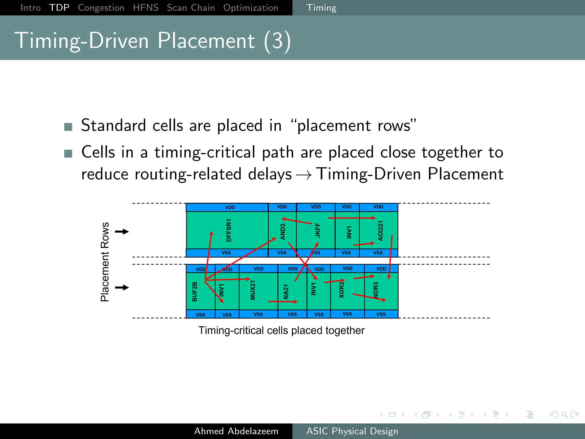
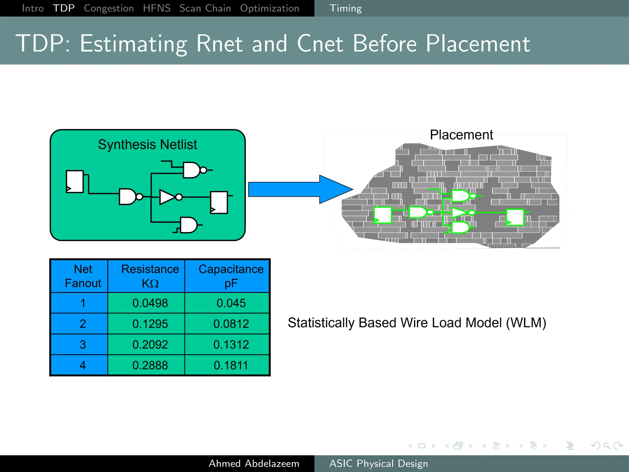
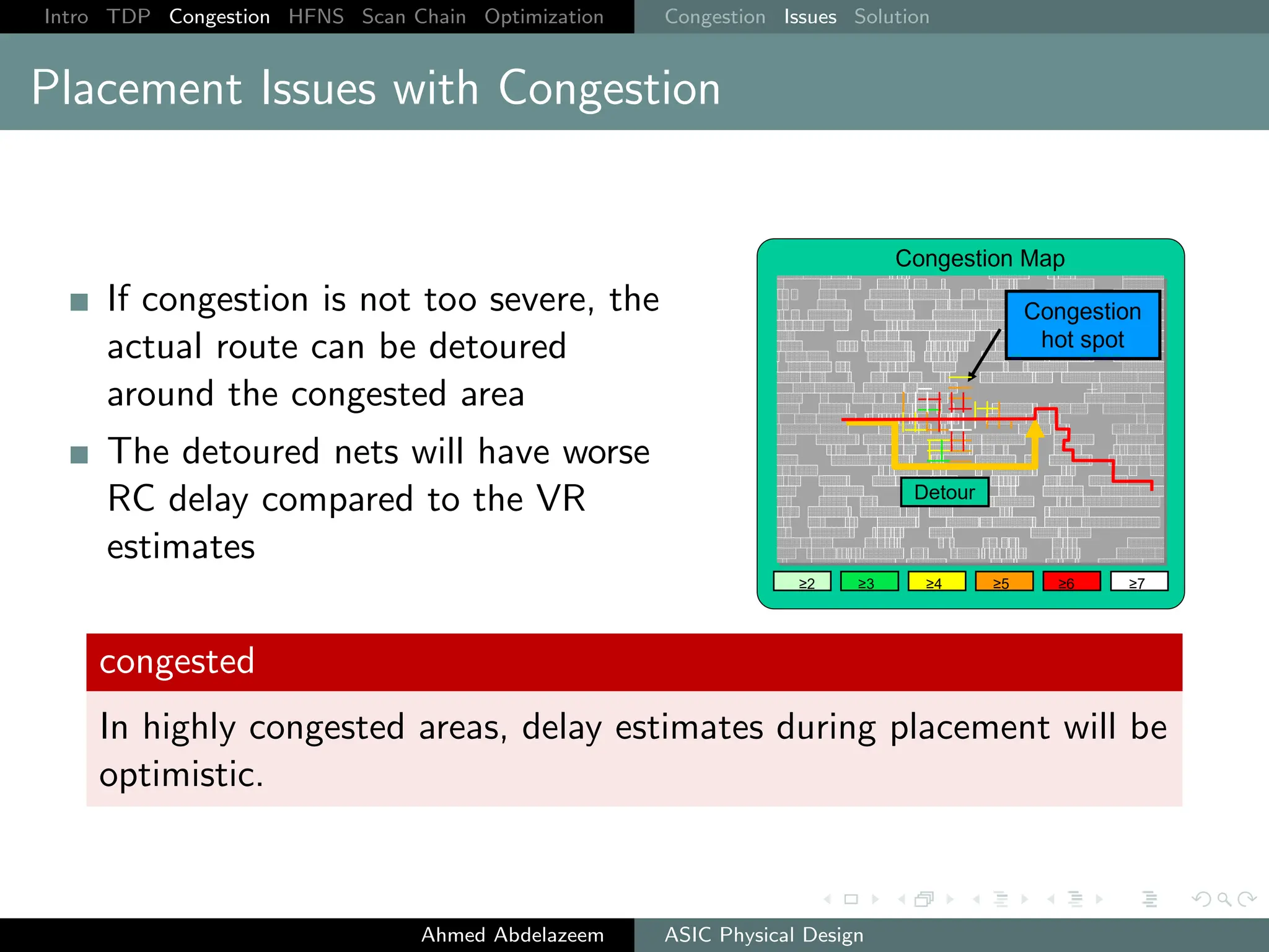
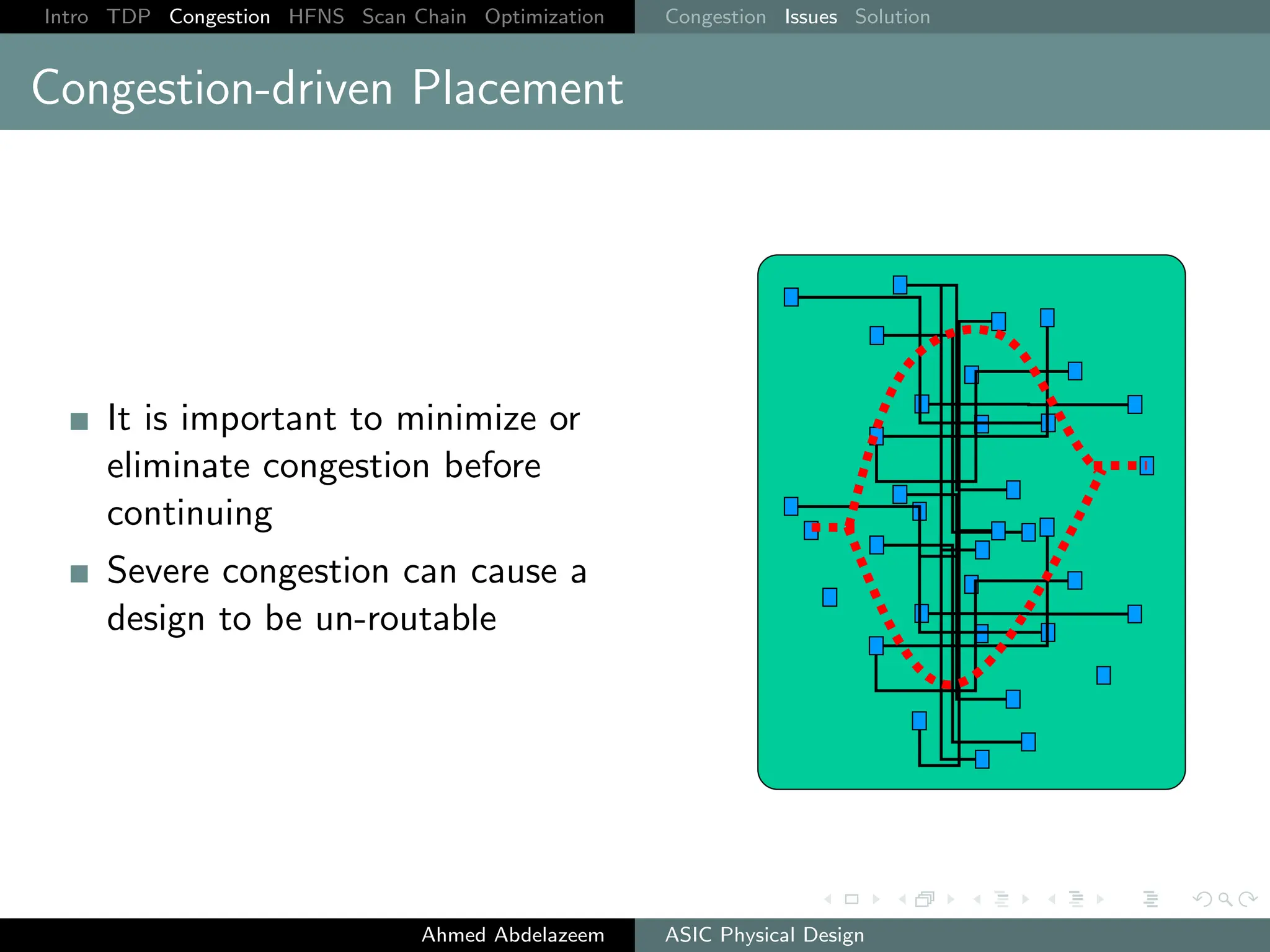
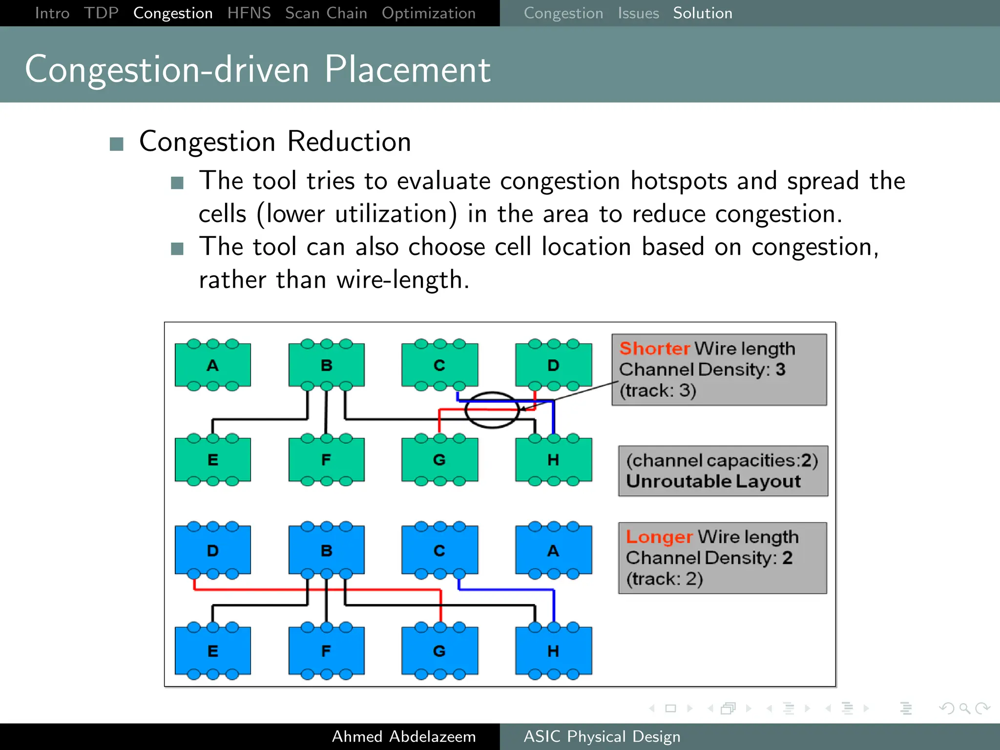
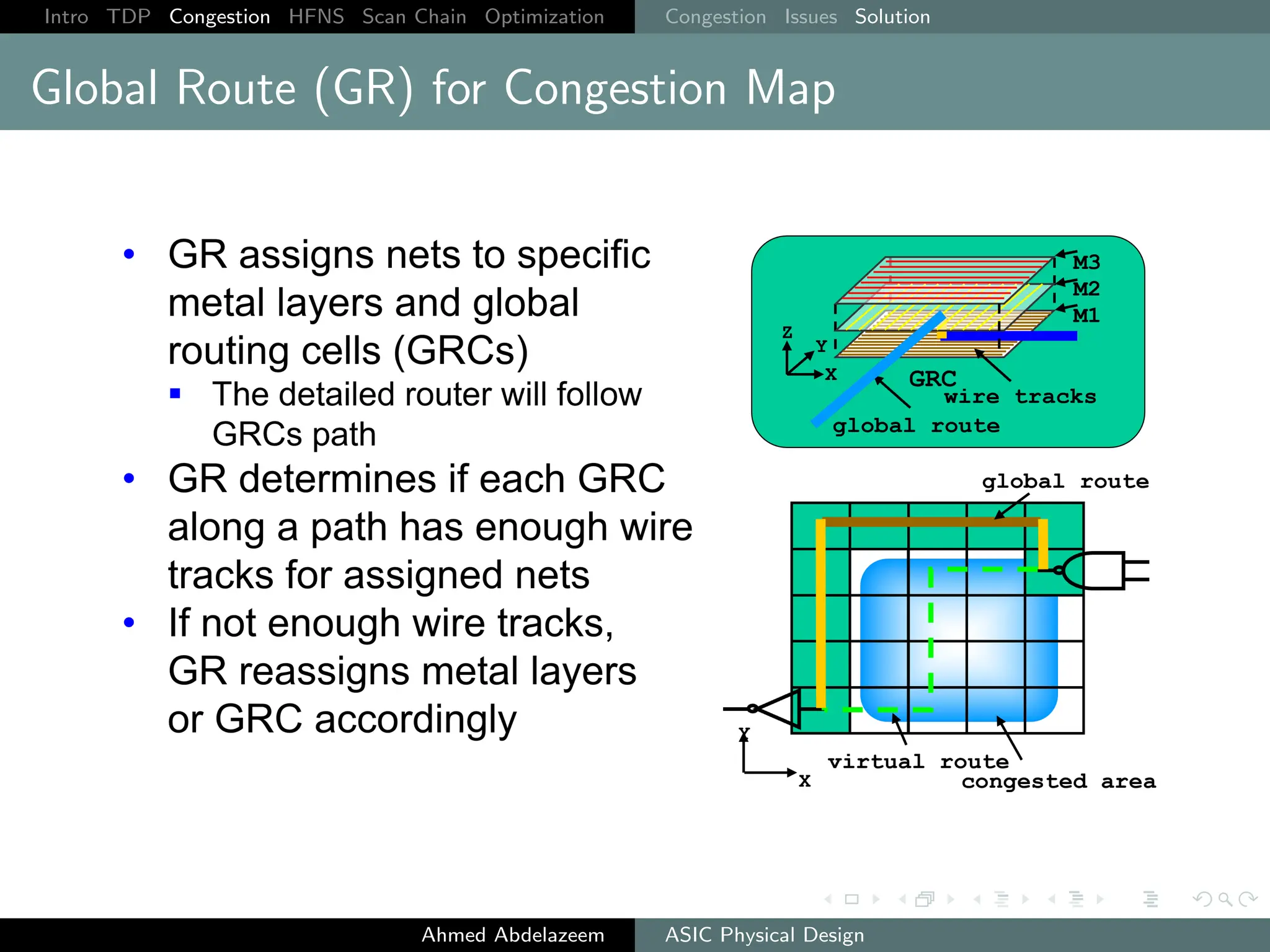
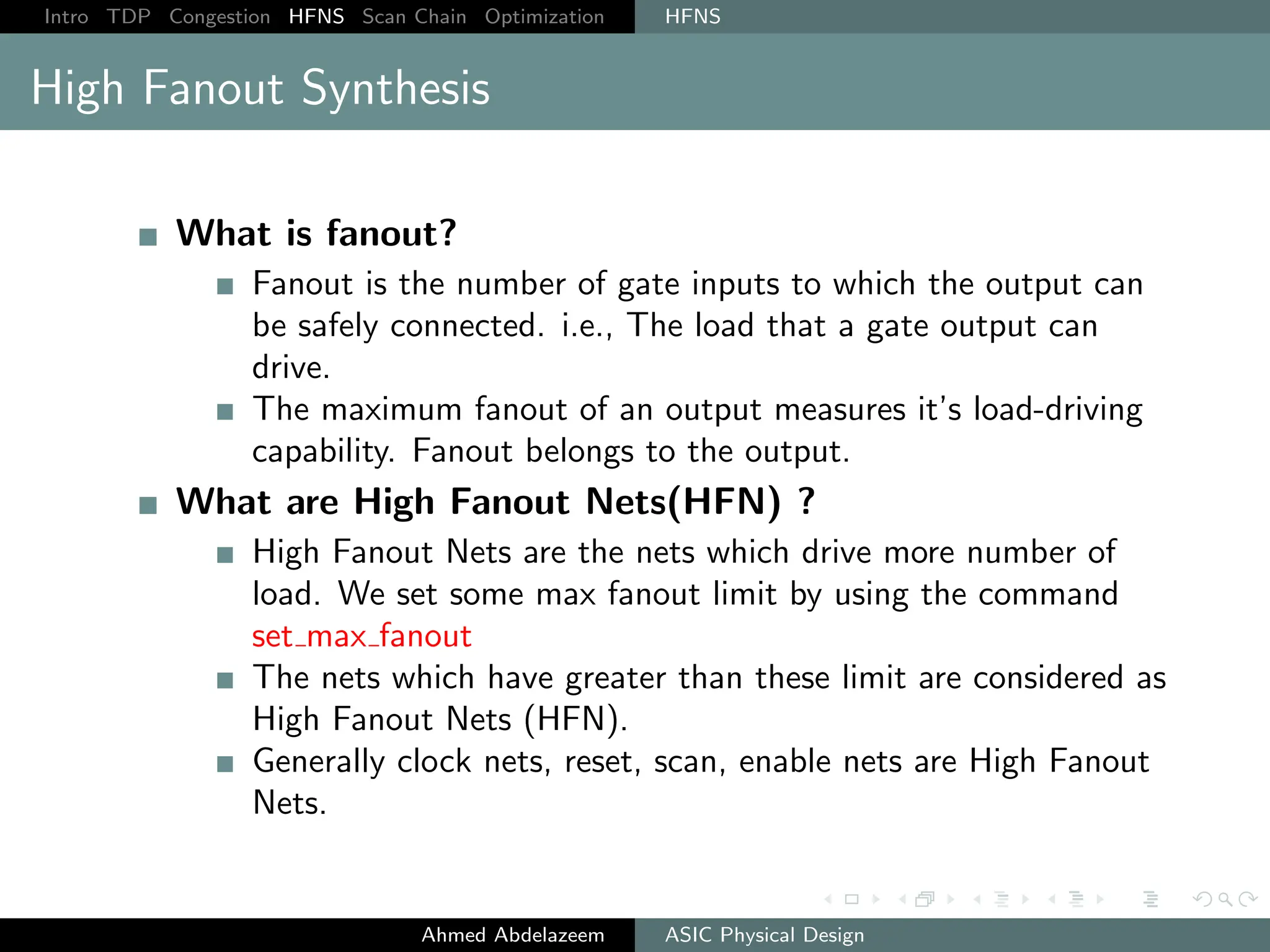
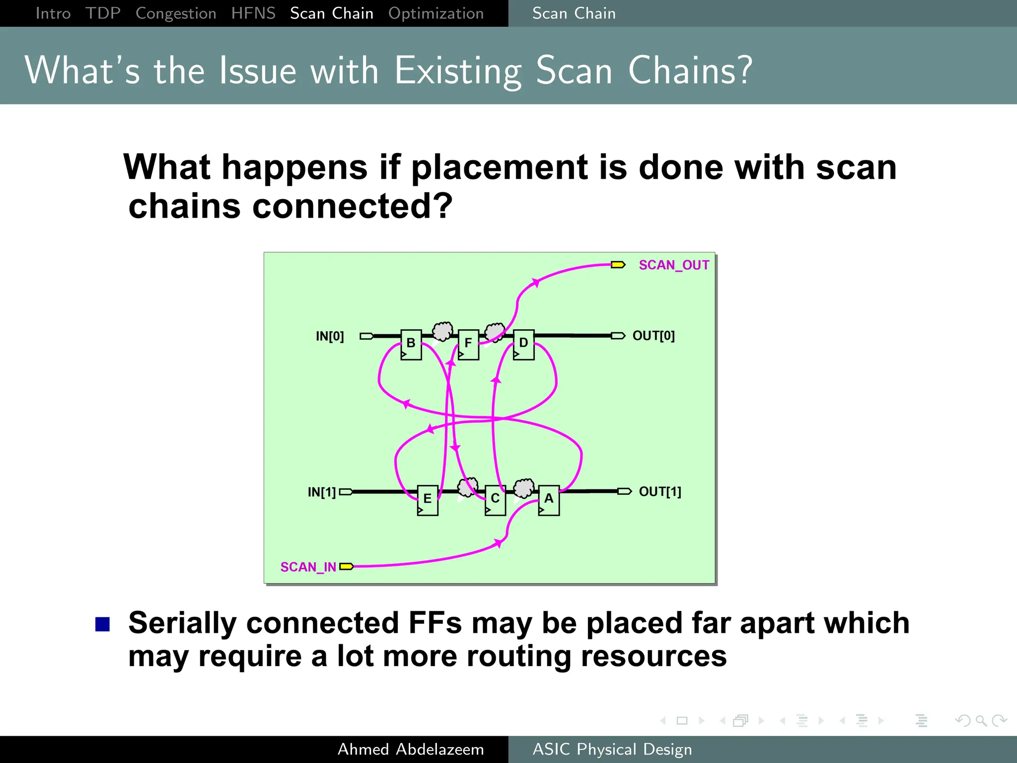
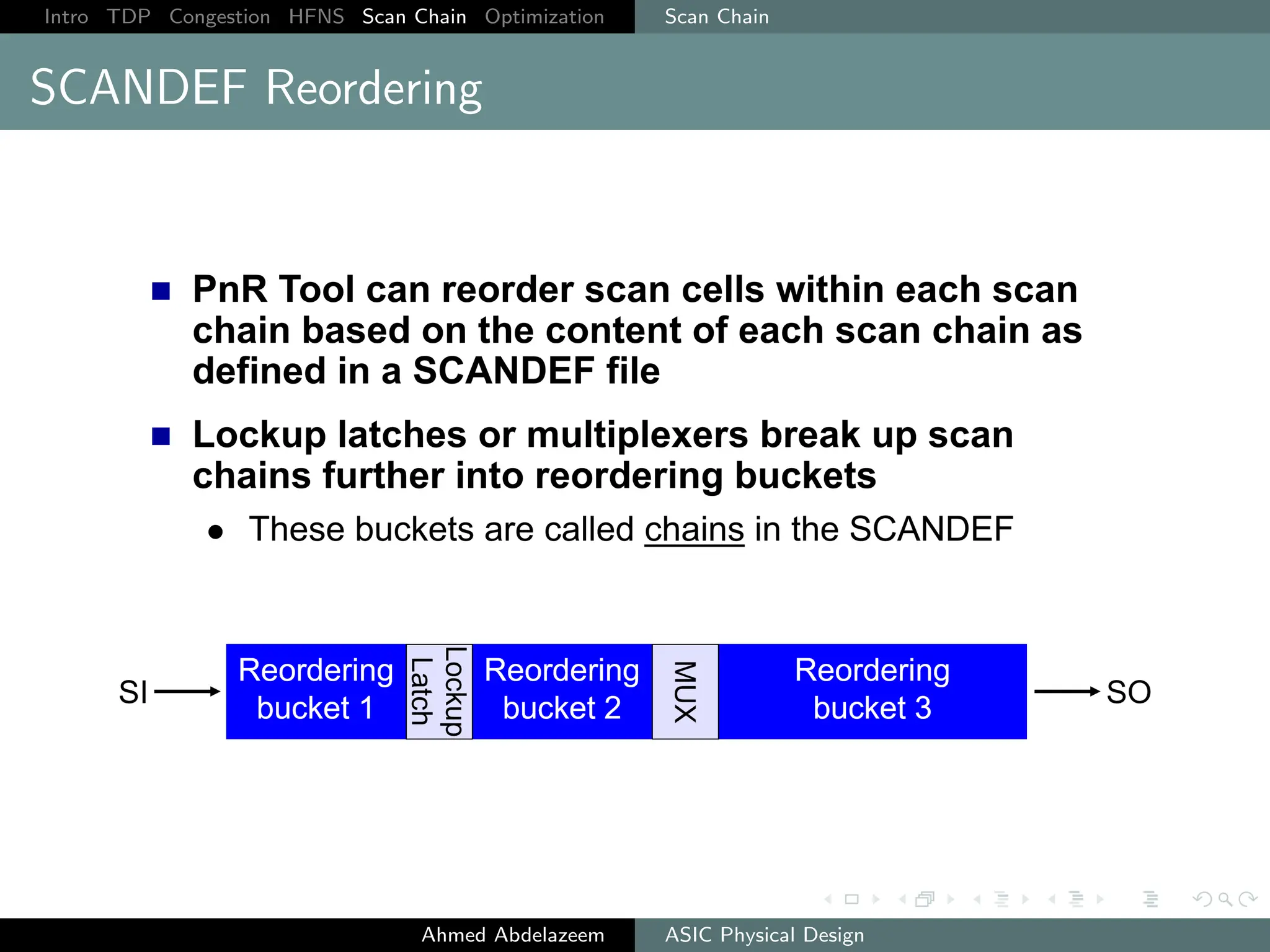
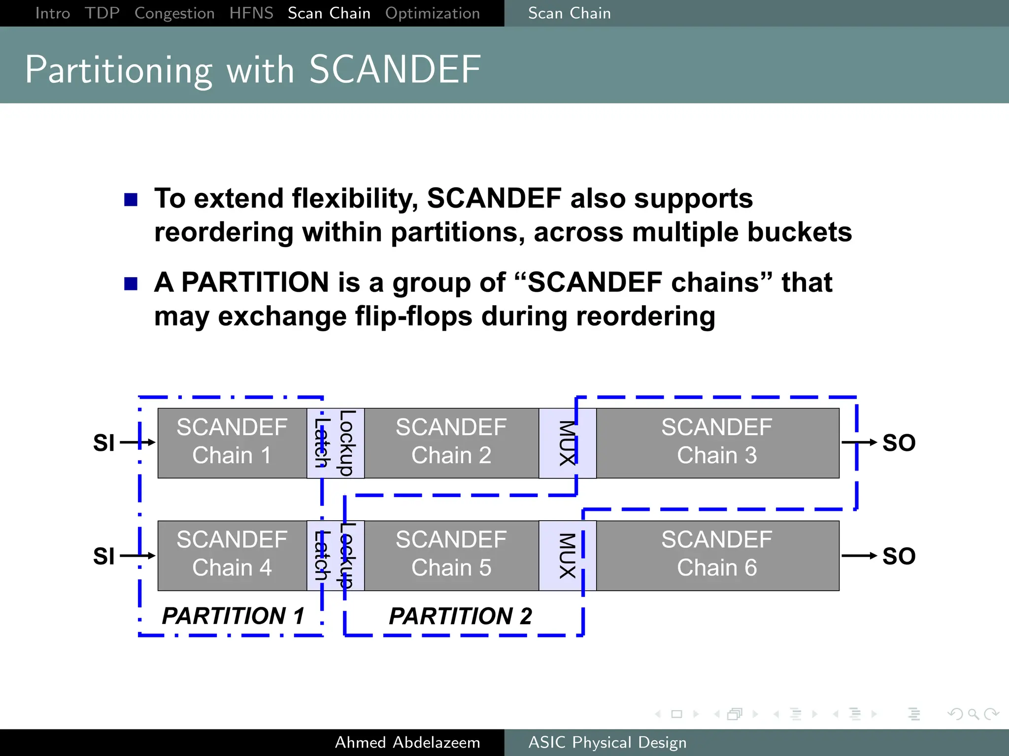
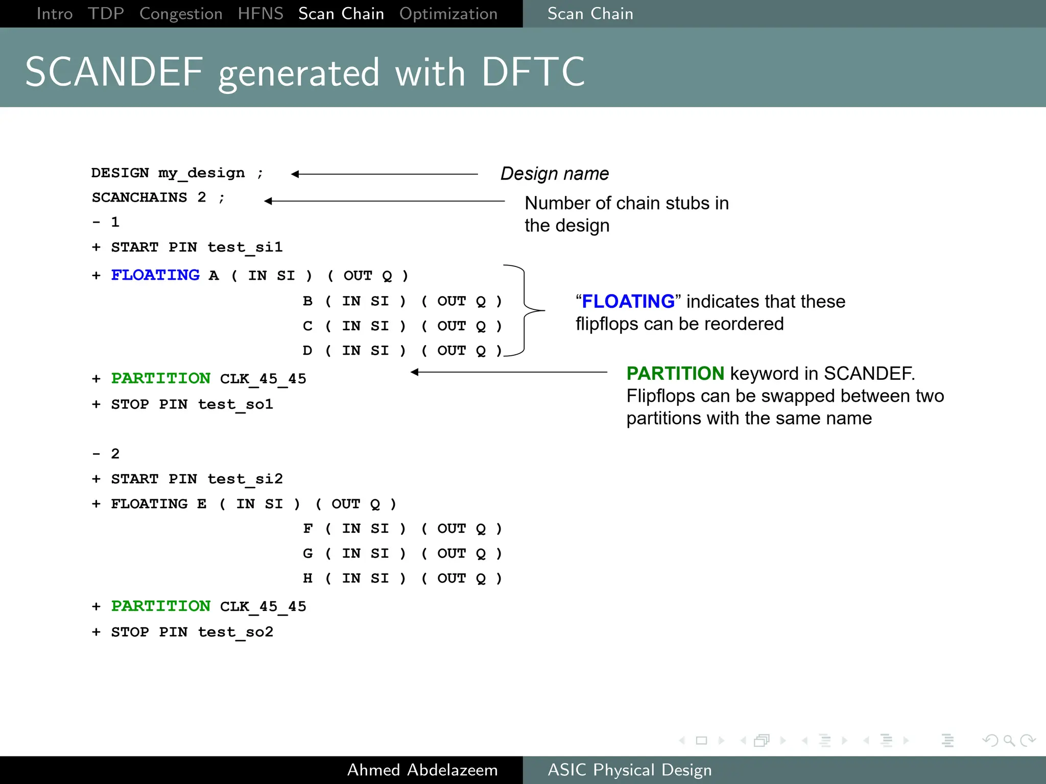
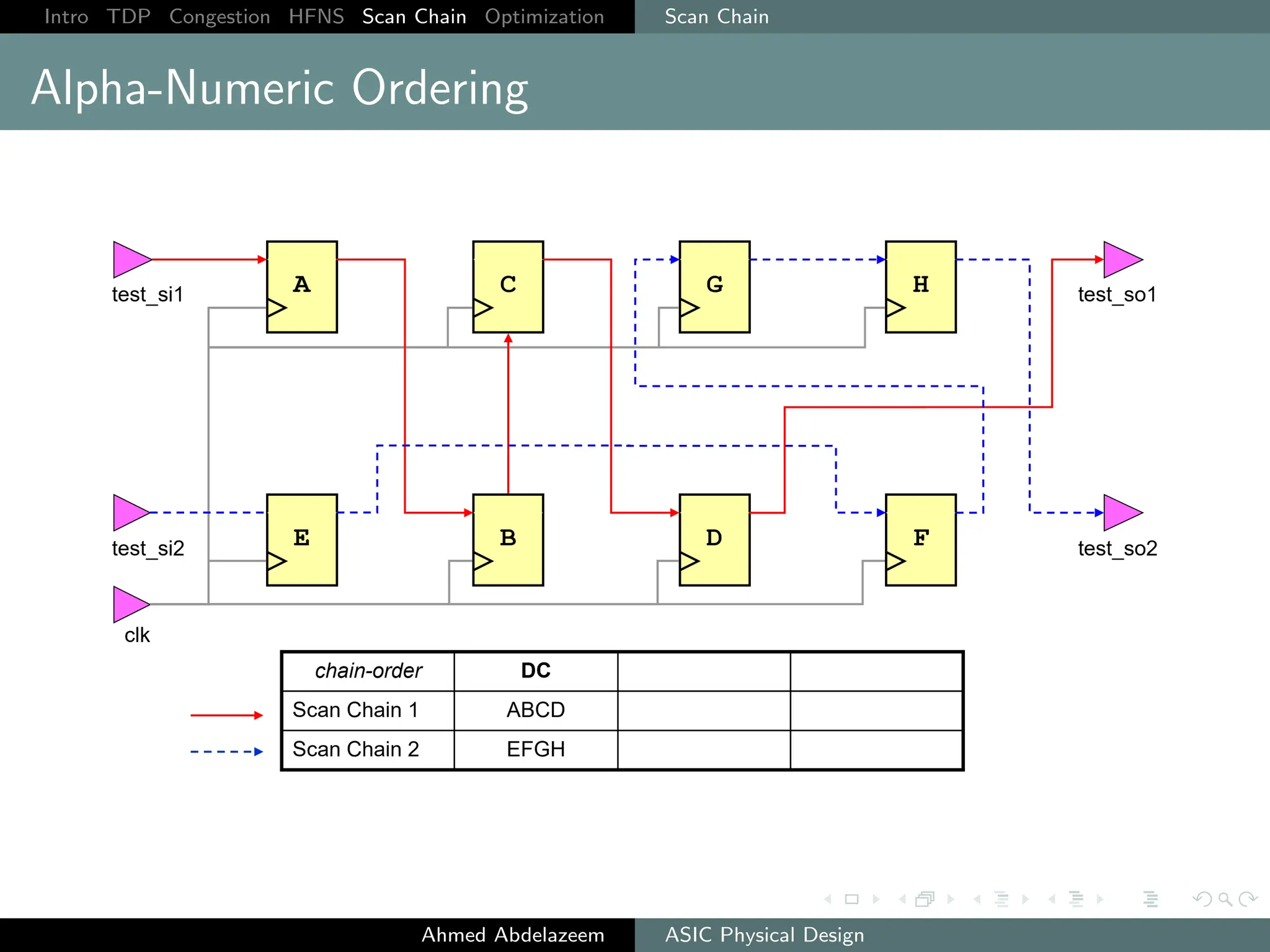
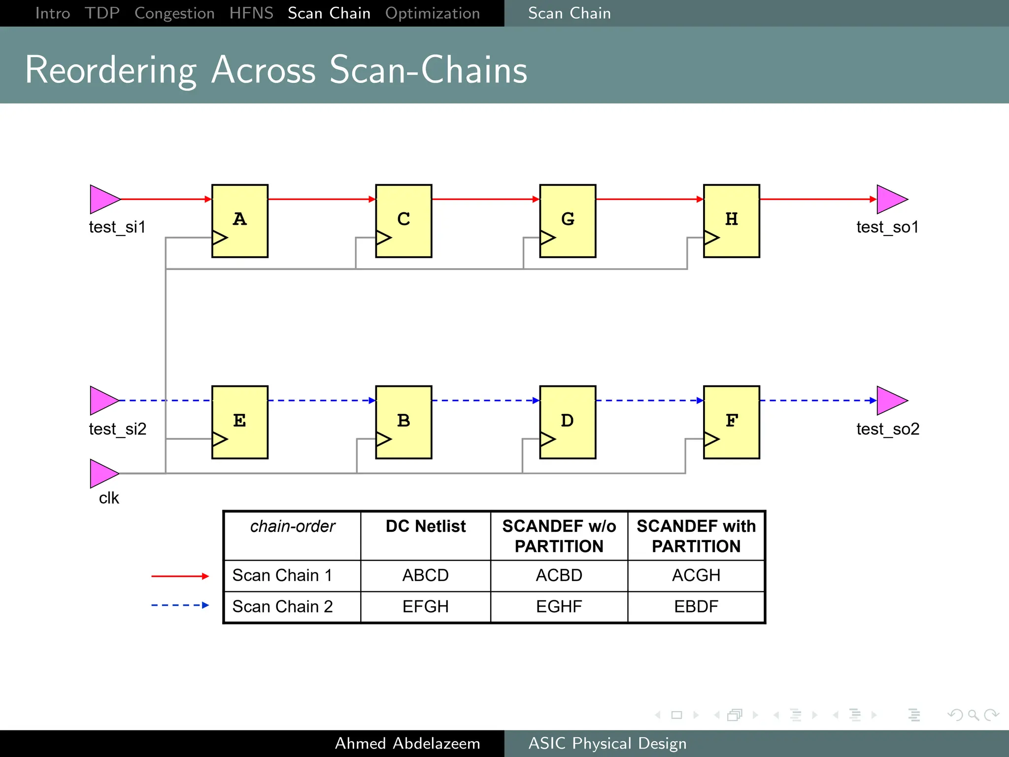
The document outlines the process of ASIC physical design and placement, particularly focusing on techniques for optimizing placement for timing and congestion. Key topics include timing-driven placement, congestion-driven placement, high fanout synthesis, and scan chain optimization, emphasizing the importance of circuit placement in modern technology nodes (65nm and below). Strategies to minimize routing congestion and ensure legal cell placement are discussed to meet timing and area constraints.


![[Back2School] STA Methodology- Chapter 7pdf](https://cdn.slidesharecdn.com/ss_thumbnails/stamethodology-250624214856-5fd24ebc-thumbnail.jpg?width=640&height=640&fit=bounds)


![[Back2School] Constraint Develop.pdf- Chapter 3](https://cdn.slidesharecdn.com/ss_thumbnails/constraintdevelop-250606153235-d8296a49-thumbnail.jpg?width=640&height=640&fit=bounds)


![[Back2School] Timing Checks- Chapter 5.pdf](https://cdn.slidesharecdn.com/ss_thumbnails/specialtimingchecks-250609185635-cf7ed43c-thumbnail.jpg?width=640&height=640&fit=bounds)


![[Back2School] Crosstalk and Noise- Chapter 6.pdf](https://cdn.slidesharecdn.com/ss_thumbnails/crosstalkandnoise-250624214313-69c347be-thumbnail.jpg?width=640&height=640&fit=bounds)
![[Back2School] Timing Verification- Chapter 4](https://cdn.slidesharecdn.com/ss_thumbnails/timingverification-250607212312-4e8e2612-thumbnail.jpg?width=640&height=640&fit=bounds)
![[Back2School] Delay Calculation- Chapter 2](https://cdn.slidesharecdn.com/ss_thumbnails/delaycalculation-250530192911-03116e20-thumbnail.jpg?width=640&height=640&fit=bounds)
![[Back2School] STA Basic Concepts- Chapter 1.pdf](https://cdn.slidesharecdn.com/ss_thumbnails/stabasicconcepts-250524204554-25ac4895-thumbnail.jpg?width=640&height=640&fit=bounds)


