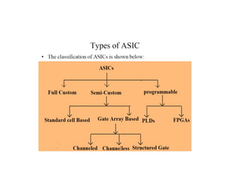
Structured Gate Arrays
•A structured gate array combines some of the features
of CBICs and MGAs.
• One of the biggest disadvantages of the MGA is the fixed
gate-array base cell. This makes the implementation of
memory, for example, inefficient or difficult.
• In a structured gate array, also called embedded gate
array, master slice or master image only the interconnect
is customized, custom blocks (the same for each design)
can be embedded and manufacturing can take from two
days to two weeks.
39.
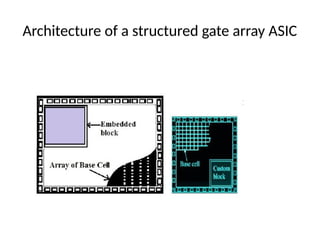
• In anembedded gate array some of the IC
area is set aside and dedicated to a specific
function.
• This embedded area can contain:
• A different base cell that is more
suitable for building memory cells, or
• Can contain a microcontroller or
another complete circuit block.
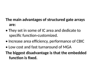
The main advantagesof structured gate arrays
are:
• They set in some of IC area and dedicate to
specific function-customized.
• Increase area efficiency, performance of CBIC
• Low cost and fast turnaround of MGA
The biggest disadvantage is that the embedded
function is fixed.
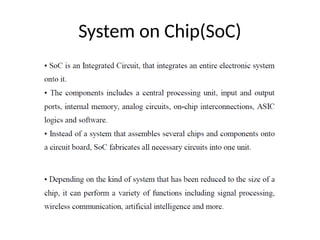
A typical SoCconsists of:
• A microcontroller, microprocessor, digital signal processor.
• Memory blocks including a selection of ROM, RAM, EEPROM, and
Flash Memory.
• Timing sources including Oscillators and PLLs.
• Peripherals including Counter-timers, real-time timers, and power-on
reset generators.
• External interfaces including industry standards such as USB, Ethernet.
• Analog interfaces including ADCs and DACs.
• SoC Bus.
• DMA controllers route data directly between external interfaces and
memory.
61.
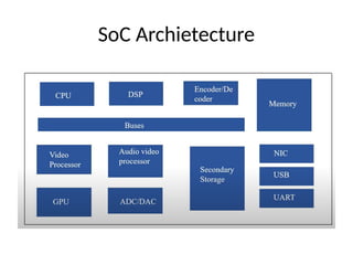
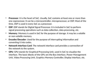
• Processor: Itis the heart of SoC. Usually, SoC contains at least one or more than
one coprocessor. It can be a microcontroller, microprocessor, or DSP. Most of the
time, DSP is used in every SoC as a processor.
• DSP: DSP stands for Digital Signal Processor. It is included in SoC to perform
signal processing operations such as data collection, data processing, etc.
• Memory: Memory is used in SoC for the purpose of storage. It may be a volatile
or non-volatile memory.
• Encoder/Decoder: Used for the purpose of interrupting information and
converting it into codes.
• Network Interface Card: The network interface card provides a connection of
the network to the system.
• GPU: GPU stands for Graphical Processing Unit, used in SoC to visualize the
interface. The basic blocks of the GPU are the Bus interface, Power Management
Unit, Video Processing Unit, Graphics Memory Controller, Display interface, etc.
62.
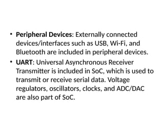
• Peripheral Devices:Externally connected
devices/interfaces such as USB, Wi-Fi, and
Bluetooth are included in peripheral devices.
• UART: Universal Asynchronous Receiver
Transmitter is included in SoC, which is used to
transmit or receive serial data. Voltage
regulators, oscillators, clocks, and ADC/DAC
are also part of SoC.
69.
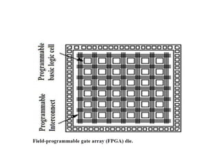
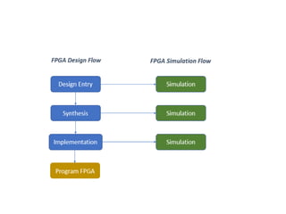
FPGA DESIGN FLOW
•A Field Programmable Gate Array, or FPGA, is a semiconductor
device that comprises of logic blocks which are programmed to
execute a specific set of functions.
• These programmable logic blocks are connected to each other
with the help of an interconnect matrix. These interconnects are
responsible for connecting the logic blocks and facilitating the
flow of signals across the chip
• This structure is arranged in the form of a two-dimensional array
consisting of logic blocks, interconnects, and I/O blocks that
connect it with the input and output signals. A logic block itself is
composed of a look up table or LUT and a flip flop or FF and a
multiplexer.
70.
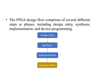
• The FPGAdesign flow comprises of several different
steps or phases, including design entry, synthesis,
implementation, and device programming.
71.
Design Entry
• Designentry can be done using various techniques, such as
schematics, through Hardware Description Language or HDL, or
you may even combine the two and use a best of both worlds
approach using tools that can convert HDL into schematics and
vice versa depending on your FPGA design and preference.
• Generally, for a design that deals more with complex systems, it
is better to opt for HDL, a quicker, language based process that
rids you of the need to design in lower level hardware, while
schematics is a good choice for someone who wishes to design
hardware because it gives more visibility to the entire system.
• You can also opt to go for a state-machines based approach, but it
is largely limited and unused currently.
• It is suited for designers who view their design as a series of
states.
72.
• While aschematic based technique is easier to read
and comprehend, it tends to only work with relatively
smaller projects.
• HDL based approaches, on the other hand, tend to be
fast and easy to implement, and today is most popular
design entry for FPGA designs.
73.
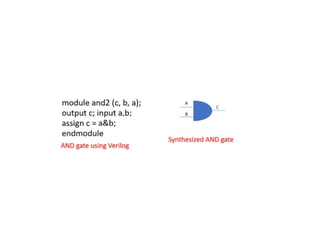
Synthesis
• After thedesign has been entered in the form of code, this phase is where it is
translated into an actual circuit with elements such as gates, flip flops, and
multipliers among others.
• Your input HDL is essentially converted into a netlist which lists the logic
elements you will be needing for your project and the interconnects needed in the
specific hierarchy
• The process begins with a syntax check once you feed in your HDL based design.
• It is then optimized by the reduction of logic, elimination of redundant logic, and
the reduction of the size of the design while simultaneously making it faster to
implement.
• The last step is to map out the technology by connecting the design to the logic,
estimating the associated time, and churning out the design netlists which are
subsequently saved.
• FPGA synthesis is performed by dedicated synthesis tools.
• Cadence, Synopsys and Mentor Graphics are EDA companies that develop, sell
and market FPGA synthesis tools.
75.
Implementation
• This phaseis where the layout of your design will be determined and consists of three
steps: translate, map, and place & route.
• The tools used in this step are provided by the FPGA vendors because they know best
how to translate a synthesized netlist into an FPGA.
• The first step for the tools is to gather all the constraints that are set by the user
together with the netlist files.
• These constraints can be regarding the assignment and position of the pins, the
requirements regarding timing such as the maximum delay or the input period of the
clock.
• Then the tool maps out the implementation by comparing the resource requirement
specified in the files to the resources actually available on the FPGA being used.
• The circuit is divided into the logic blocks or elements in the form of sub blocks. As a
result, your entire design is placed in specific logic blocks and is ‘mapped out’ into the
FPGA
• The next step is to connect and route all the signals accordance with the constraints set
by the user between all the logic blocks and IO blocks.
• Tools provided by FPGA vendors (e.g., Xilinx Vivado, Intel Quartus, Lattice Diamond).
76.
Device Programming
• Thelast step in the process is to finally load
the mapped out and completely routed design
into the FPGA.
• For that reason, you will need a to generate a
BitSteam file.
• The Bitstream file is transferred to the FPGA
using programming hardware/software tools
provided by the FPGA vendor.
77.
FPGA Verification &Simulation
• At the end of each step in the FPGA design
flow, you have the opportunity to simulate
and test you design.
• There are essentially 3 points allowed by the
FPGA design flow: at design entry, post
synthesis, or post implementation.
78.
Behavioral Simulation (AtDesign Entry)
• Behavioral simulation, called also (Register
Transfer Level) RTL simulation, is performed
before synthesis.
• This fast simulation can be used to check the
functionality of the design without constraints.
• Use this simulation frequently to test your code
and find logic errors.
79.
Functional Simulation (PostSynthesis)
• The functionality the design can be verified
using functional simulation after the synthesis
process has completed.
• It is a netlist level simulation that ignore
timing related issues.
80.
Timing Simulation (AtImplementation)
• This simulation will give you the most accurate
picture of your design behavior.
• It takes into account the target FPGA chip and all
the logic blocks functionality, wiring, delays and
much more.
• Timing simulation takes longer time and provides
much more details than the previous simulation.
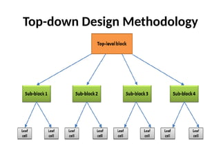
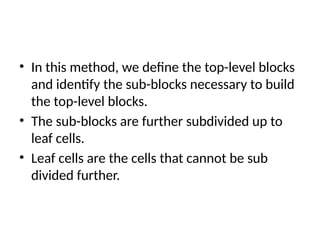
• In thismethod, we define the top-level blocks
and identify the sub-blocks necessary to build
the top-level blocks.
• The sub-blocks are further subdivided up to
leaf cells.
• Leaf cells are the cells that cannot be sub
divided further.
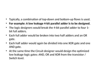
• Typically, acombination of top-down and bottom-up flows is used.
• For example: A low leakage 4-bit parallel adder is to be designed.
• The logic designers would break the 4-bit parallel adder to four 1-
bit full adders.
• Each full adder would be broken into two half adders and an OR
gate.
• Each half adder would again be divided into one XOR gate and one
AND gate.
• At the same time the Circuit designer would design the optimized
low leakage logic gates: AND, OR and XOR from the transistor /
Switch level.