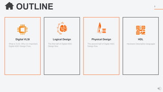
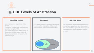
RTL DESIGN
with VHDL
101
S E S S I O N 0 1
D I G I T A L V L S I T O P I C S
W W W . Y O U T U B E . C O M / C H A N N E L / U C C E C V 3 G Q L Q C R T 8 M S 3 _ A R N 9 Q
For all course videos and material visit YouTube channel
W W W . L I N K E D I N . C O M / I N / M A H M O U D A B D E L L A T I F
3
What is VLSI, Why it is Important,
Digital ASIC Design Flow..
Digital VLSI
The first half of Digital ASIC
Design flow
Logical Design
The second half of Digital ASIC
Design flow
Physical Design
Hardware Description languages
HDL
OUTLINE
4
D I G I T A L D E S I G N F L O W
Digital VLSI
S E S S I O N 0 1
VLSI Industry
5
V L S I
https://www.linkedin.com/pulse/vlsi-industry-orientation-session-undergrad-egypt-abdellatif/
U S E F U L L I N K S
We can now fabricate millions of
transistors in a unit square inch piece of
silicon 
Very Large Scale Integration (VLSI).
To facilitate this complex design and
fabrication of an IC, various automatic
tools and machines are available for
design and verification of an IC 
A Electronic Design Automation (EDA)
software tools.
S E S S I O N 0 1
Digital ASIC Design Flow
6
V L S I
Logical
Design
Physical
Design
DESIGN SYNTHESIS LAYOUT TAPEOUT
7
D I G I T A L D E S I G N F L O W
Logical Design
S E S S I O N 0 1
Logical Design
8
V L S I
• The flow starts with High-Level design Specification.
• The designer defines Area, Speed and Power constraints under which the goal has to be achieved.
Design
Specification
Logical Design
…. Design
…….. Design Specification
S E S S I O N 0 1
Logical Design
9
V L S I
• The designer starts thinking about the architectural design
• The design functionality is broken down to small pieces with clear understanding about the block
implementation
• Each design has objectives and constraints
• Functionality • Speed at which a design can operate • Power consumed by the design
• Testability of the design • Area of chip package
System
Architecture
Logical Design
…. Design
…….. System Architecture
S E S S I O N 0 1
Logical Design
1 0
V L S I
RTL
Design
RTL, Register Transfer Level, describing the functional behavior using HDL, hardware description
languages, VHDL, Verilog or SystemVerilog .
Logical Design
…. Design
…….. RTL Design
S E S S I O N 0 1
Logical Design
1 1
V L S I
Functional Verification, verifying the functionality using simulation.
Functional
Verification
Logical Design
…. Design
…….. Functional Verification
S E S S I O N 0 1
Logical Design
1 2
V L S I
Logic
Synthesis
• The first step of converting the RTL to Gate Netlist.
• Synthesis tool takes a Standard Cell Library, Constraints, RTL codes and generate Gate Level
Netlist.
• Timing, Power and Area constraints are guiding synthesis tools to achieve design goals.
Logical Design
…. Synthesis
…….. Logic Synthesis
S E S S I O N 0 1
Logical Design
1 3
V L S I
Design
For Test
DFT, this step is for preparing the design for testability. Scan insertion is a common technique that
helps to make all registers in the design controllable and observable.
Logical Design
…. Synthesis
…….. Design for Testability
S E S S I O N 0 1
Logical Design
1 4
V L S I
This is used to verify the functionality of gate netlist against the RTL description using formal
verification techniques.
Equivalence
Checking
Logical Design
…. Synthesis
…….. Equivalence Checking
S E S S I O N 0 1
Logical Design
1 5
V L S I
Static
Timing
Analysis
STA, static timing analysis, a method of checking the ability of the design to meet the timing
requirements statically without simulation.
The designer is responsible of specifying 'Timing Constraints' to model how the design needs to be
constrained & the STA tools check that the design meets the timing requirements.
The designer uses an industry standard format 'SDC' Synopsys Design Constraints.
STA on this stage acts as the bridge between logical and physical design
Logical Design
…. Synthesis
…….. Static Timing Analysis
1 6
D I G I T A L D E S I G N F L O W
Physical Design
S E S S I O N 0 1
Physical Design
1 7
V L S I
Floor
Planning
• Floor planning is the starting step in ASIC physical design
• The logical blocks locations are determined considering many optimization factors to account for Area,
Speed and Power
• These parameters are decided in this stage.
- Die size, core size of the chip - I/O pad’s location
- Plan for power
Physical Design
…. Layout
…….. Floor Planning
S E S S I O N 0 1
Physical Design
1 8
V L S I
Placement
• Assigning exact locations for the blocks within the chip core area
• A placement tool takes a given synthesized circuit netlist together with a technology library and
produces a valid placement layout
Physical Design
…. Layout
…….. Placement
S E S S I O N 0 1
Physical Design
1 9
V L S I
Clock
Tree
Synthesis
• Clock Tree Synthesis ‘CTS’ is the step which is responsible for distributing the clock and reduce
clock skew between different parts of the design by insertion of buffers or inverters along the
clock paths of ASIC design.
Physical Design
…. Layout
…….. Clock Tree Synthesis
S E S S I O N 0 1
Physical Design
2 0
V L S I
Routing
• Routing the design is the final step to generate the layout.
• During the physical design, STA may be done multiple times to perform a more accurate timing
analysis.
•
Physical Design
…. Layout
…….. Routing
S E S S I O N 0 1
Physical Design
2 1
V L S I
Signoff
LVS
Two steps are needed to verify the layout
• LVS, Layout versus Netlist, matching the layout with the gate level netlist generated after
synthesis.
Physical Design
…. Tapeout
…….. LVS
S E S S I O N 0 1
Physical Design
2 2
V L S I
Signoff
DRC
• DRC, Design Rule Checking, All rules laid out by the foundry where it will be fabricated into a chip
are adhered
• For Example
If two metal wires are too close together on the same layer, they may short during the
manufacturing process
Physical Design
…. Tapeout
…….. DRC
S E S S I O N 0 1
Physical Design
2 3
V L S I
Signoff
STA
• Signoff Static Timing Analysis is performed again at this phase.
Physical Design
…. Tapeout
…….. Signoff STA
S E S S I O N 0 1
Physical Design
2 4
V L S I
GDSII
Release
• Fabs manufacture ICs based on the GDSII
• GDSII stream format is the industry standard for data exchange of IC layout.
• This Digital ASIC design flow is referred to as RTL2GDSII flow & the process to generate GDSII is
termed as Tapeout.
Physical Design
…. Tapeout
…….. GDSII Release
2 5
D I G I T A L D E S I G N F L O W
Hardware Description
Languages
S E S S I O N 0 1
Hardware Description Language
2 6
V L S I
There are two popular widely used HDL languages
• VHDL
- first version came in 1987 followed by versions 1993, 2000, 2002, 2006 and 2008
- more difficult to learn
- strongly typed
- 85% of FPGA designs done in VHDL
• Verilog
- first version in 1985 followed by versions 1995, 2001, 2005 and SystemVerilog
- easier and simpler to learn
- weakly typed
- 85% of ASIC designs done with Verilog
If you learn VHDL then you can learn Verilog in few weeks
If you learn Verilog then it may be hardware to accept learning VHDL
S E S S I O N 0 1
HDL Levels of Abstraction
2 7
V L S I
Used to describe algorithms of the
design.
This is the highest level of abstraction
possible using the HDL.
The top level function of the design is
described and it is useful mainly at
the system analysis, simulation and
partition stage.
Behavioral Design
RTL design comes in between behavioral.
It has detailed description of the circuit
with respect to the clocks and data flow.
RTL Design
This is closer to physical representation of
a circuit and has almost zero abstraction.
This form of HDL is generally the output of
a synthesis tool which takes RTL design
as input.
Gate Level Netlist
MODELING
RTL
Design
Netlist
S E S S I O N 0 1
HDL STRUCTURE
2 8
V L S I
PACKAGE
DECLARATION
____________
PACKAGE BODY
(used for functions,
constants,
components,…)
ENTITY
(Interface Description)
ARCHITECTURE
(Functionality)
Concurrency Nature
You have to think in Hardware when you write your
VHDL/Verilog code
In this code, both AND & OR gates works at the same
time and any update on x reflects on e at the same time
BEGIN
x <= A AND B;
e <= x OR y;
END;
X
y
e
M A N Y T H A N K S
Session 01 _rtl_design_with_vhdl 101

Session 01 _rtl_design_with_vhdl 101

  • 1.
    RTL DESIGN with VHDL 101 SE S S I O N 0 1 D I G I T A L V L S I T O P I C S
  • 2.
    W W W. Y O U T U B E . C O M / C H A N N E L / U C C E C V 3 G Q L Q C R T 8 M S 3 _ A R N 9 Q For all course videos and material visit YouTube channel W W W . L I N K E D I N . C O M / I N / M A H M O U D A B D E L L A T I F
  • 3.
    3 What is VLSI,Why it is Important, Digital ASIC Design Flow.. Digital VLSI The first half of Digital ASIC Design flow Logical Design The second half of Digital ASIC Design flow Physical Design Hardware Description languages HDL OUTLINE
  • 4.
    4 D I GI T A L D E S I G N F L O W Digital VLSI
  • 5.
    S E SS I O N 0 1 VLSI Industry 5 V L S I https://www.linkedin.com/pulse/vlsi-industry-orientation-session-undergrad-egypt-abdellatif/ U S E F U L L I N K S We can now fabricate millions of transistors in a unit square inch piece of silicon  Very Large Scale Integration (VLSI). To facilitate this complex design and fabrication of an IC, various automatic tools and machines are available for design and verification of an IC  A Electronic Design Automation (EDA) software tools.
  • 6.
    S E SS I O N 0 1 Digital ASIC Design Flow 6 V L S I Logical Design Physical Design DESIGN SYNTHESIS LAYOUT TAPEOUT
  • 7.
    7 D I GI T A L D E S I G N F L O W Logical Design
  • 8.
    S E SS I O N 0 1 Logical Design 8 V L S I • The flow starts with High-Level design Specification. • The designer defines Area, Speed and Power constraints under which the goal has to be achieved. Design Specification Logical Design …. Design …….. Design Specification
  • 9.
    S E SS I O N 0 1 Logical Design 9 V L S I • The designer starts thinking about the architectural design • The design functionality is broken down to small pieces with clear understanding about the block implementation • Each design has objectives and constraints • Functionality • Speed at which a design can operate • Power consumed by the design • Testability of the design • Area of chip package System Architecture Logical Design …. Design …….. System Architecture
  • 10.
    S E SS I O N 0 1 Logical Design 1 0 V L S I RTL Design RTL, Register Transfer Level, describing the functional behavior using HDL, hardware description languages, VHDL, Verilog or SystemVerilog . Logical Design …. Design …….. RTL Design
  • 11.
    S E SS I O N 0 1 Logical Design 1 1 V L S I Functional Verification, verifying the functionality using simulation. Functional Verification Logical Design …. Design …….. Functional Verification
  • 12.
    S E SS I O N 0 1 Logical Design 1 2 V L S I Logic Synthesis • The first step of converting the RTL to Gate Netlist. • Synthesis tool takes a Standard Cell Library, Constraints, RTL codes and generate Gate Level Netlist. • Timing, Power and Area constraints are guiding synthesis tools to achieve design goals. Logical Design …. Synthesis …….. Logic Synthesis
  • 13.
    S E SS I O N 0 1 Logical Design 1 3 V L S I Design For Test DFT, this step is for preparing the design for testability. Scan insertion is a common technique that helps to make all registers in the design controllable and observable. Logical Design …. Synthesis …….. Design for Testability
  • 14.
    S E SS I O N 0 1 Logical Design 1 4 V L S I This is used to verify the functionality of gate netlist against the RTL description using formal verification techniques. Equivalence Checking Logical Design …. Synthesis …….. Equivalence Checking
  • 15.
    S E SS I O N 0 1 Logical Design 1 5 V L S I Static Timing Analysis STA, static timing analysis, a method of checking the ability of the design to meet the timing requirements statically without simulation. The designer is responsible of specifying 'Timing Constraints' to model how the design needs to be constrained & the STA tools check that the design meets the timing requirements. The designer uses an industry standard format 'SDC' Synopsys Design Constraints. STA on this stage acts as the bridge between logical and physical design Logical Design …. Synthesis …….. Static Timing Analysis
  • 16.
    1 6 D IG I T A L D E S I G N F L O W Physical Design
  • 17.
    S E SS I O N 0 1 Physical Design 1 7 V L S I Floor Planning • Floor planning is the starting step in ASIC physical design • The logical blocks locations are determined considering many optimization factors to account for Area, Speed and Power • These parameters are decided in this stage. - Die size, core size of the chip - I/O pad’s location - Plan for power Physical Design …. Layout …….. Floor Planning
  • 18.
    S E SS I O N 0 1 Physical Design 1 8 V L S I Placement • Assigning exact locations for the blocks within the chip core area • A placement tool takes a given synthesized circuit netlist together with a technology library and produces a valid placement layout Physical Design …. Layout …….. Placement
  • 19.
    S E SS I O N 0 1 Physical Design 1 9 V L S I Clock Tree Synthesis • Clock Tree Synthesis ‘CTS’ is the step which is responsible for distributing the clock and reduce clock skew between different parts of the design by insertion of buffers or inverters along the clock paths of ASIC design. Physical Design …. Layout …….. Clock Tree Synthesis
  • 20.
    S E SS I O N 0 1 Physical Design 2 0 V L S I Routing • Routing the design is the final step to generate the layout. • During the physical design, STA may be done multiple times to perform a more accurate timing analysis. • Physical Design …. Layout …….. Routing
  • 21.
    S E SS I O N 0 1 Physical Design 2 1 V L S I Signoff LVS Two steps are needed to verify the layout • LVS, Layout versus Netlist, matching the layout with the gate level netlist generated after synthesis. Physical Design …. Tapeout …….. LVS
  • 22.
    S E SS I O N 0 1 Physical Design 2 2 V L S I Signoff DRC • DRC, Design Rule Checking, All rules laid out by the foundry where it will be fabricated into a chip are adhered • For Example If two metal wires are too close together on the same layer, they may short during the manufacturing process Physical Design …. Tapeout …….. DRC
  • 23.
    S E SS I O N 0 1 Physical Design 2 3 V L S I Signoff STA • Signoff Static Timing Analysis is performed again at this phase. Physical Design …. Tapeout …….. Signoff STA
  • 24.
    S E SS I O N 0 1 Physical Design 2 4 V L S I GDSII Release • Fabs manufacture ICs based on the GDSII • GDSII stream format is the industry standard for data exchange of IC layout. • This Digital ASIC design flow is referred to as RTL2GDSII flow & the process to generate GDSII is termed as Tapeout. Physical Design …. Tapeout …….. GDSII Release
  • 25.
    2 5 D IG I T A L D E S I G N F L O W Hardware Description Languages
  • 26.
    S E SS I O N 0 1 Hardware Description Language 2 6 V L S I There are two popular widely used HDL languages • VHDL - first version came in 1987 followed by versions 1993, 2000, 2002, 2006 and 2008 - more difficult to learn - strongly typed - 85% of FPGA designs done in VHDL • Verilog - first version in 1985 followed by versions 1995, 2001, 2005 and SystemVerilog - easier and simpler to learn - weakly typed - 85% of ASIC designs done with Verilog If you learn VHDL then you can learn Verilog in few weeks If you learn Verilog then it may be hardware to accept learning VHDL
  • 27.
    S E SS I O N 0 1 HDL Levels of Abstraction 2 7 V L S I Used to describe algorithms of the design. This is the highest level of abstraction possible using the HDL. The top level function of the design is described and it is useful mainly at the system analysis, simulation and partition stage. Behavioral Design RTL design comes in between behavioral. It has detailed description of the circuit with respect to the clocks and data flow. RTL Design This is closer to physical representation of a circuit and has almost zero abstraction. This form of HDL is generally the output of a synthesis tool which takes RTL design as input. Gate Level Netlist MODELING RTL Design Netlist
  • 28.
    S E SS I O N 0 1 HDL STRUCTURE 2 8 V L S I PACKAGE DECLARATION ____________ PACKAGE BODY (used for functions, constants, components,…) ENTITY (Interface Description) ARCHITECTURE (Functionality) Concurrency Nature You have to think in Hardware when you write your VHDL/Verilog code In this code, both AND & OR gates works at the same time and any update on x reflects on e at the same time BEGIN x <= A AND B; e <= x OR y; END; X y e
  • 29.
    M A NY T H A N K S