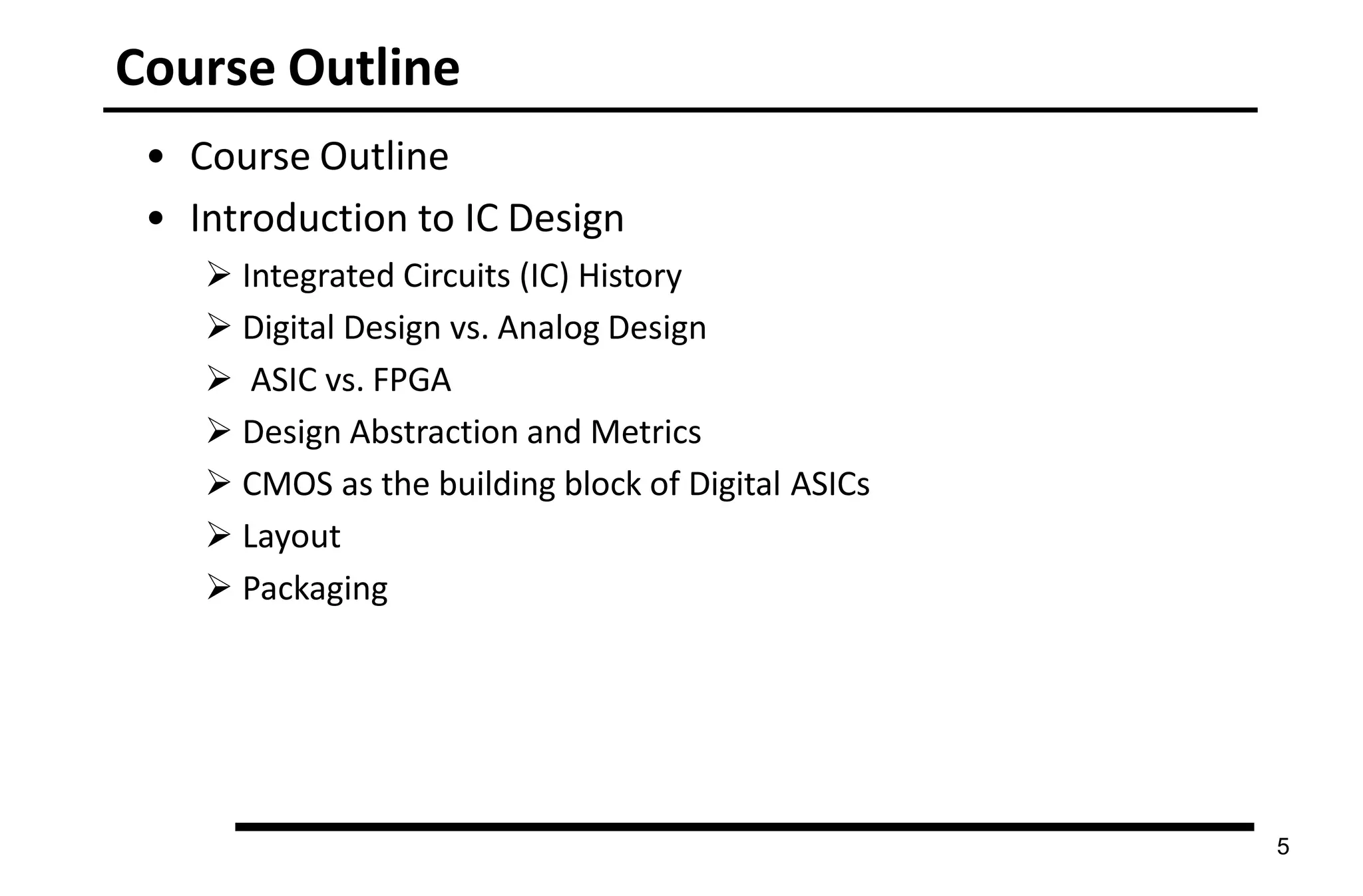
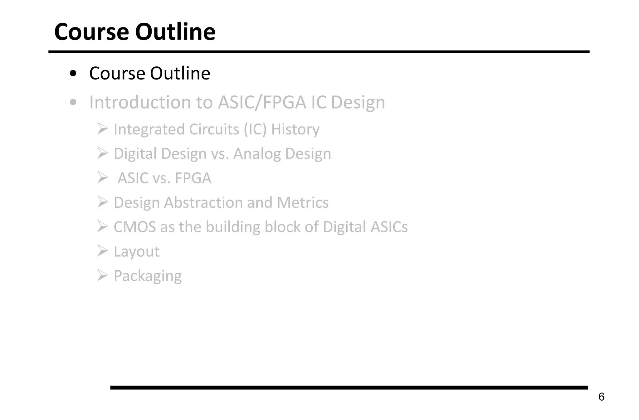
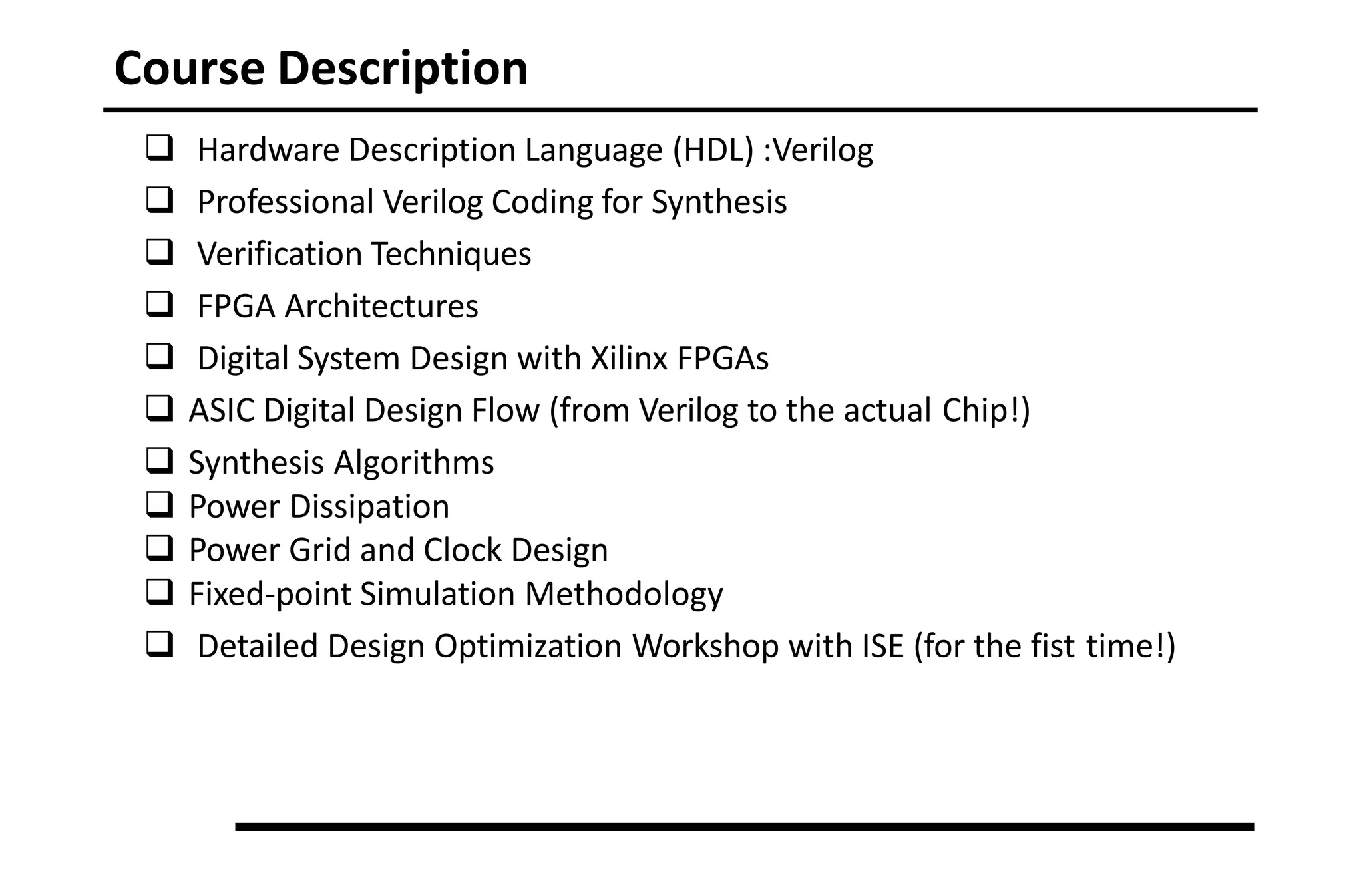
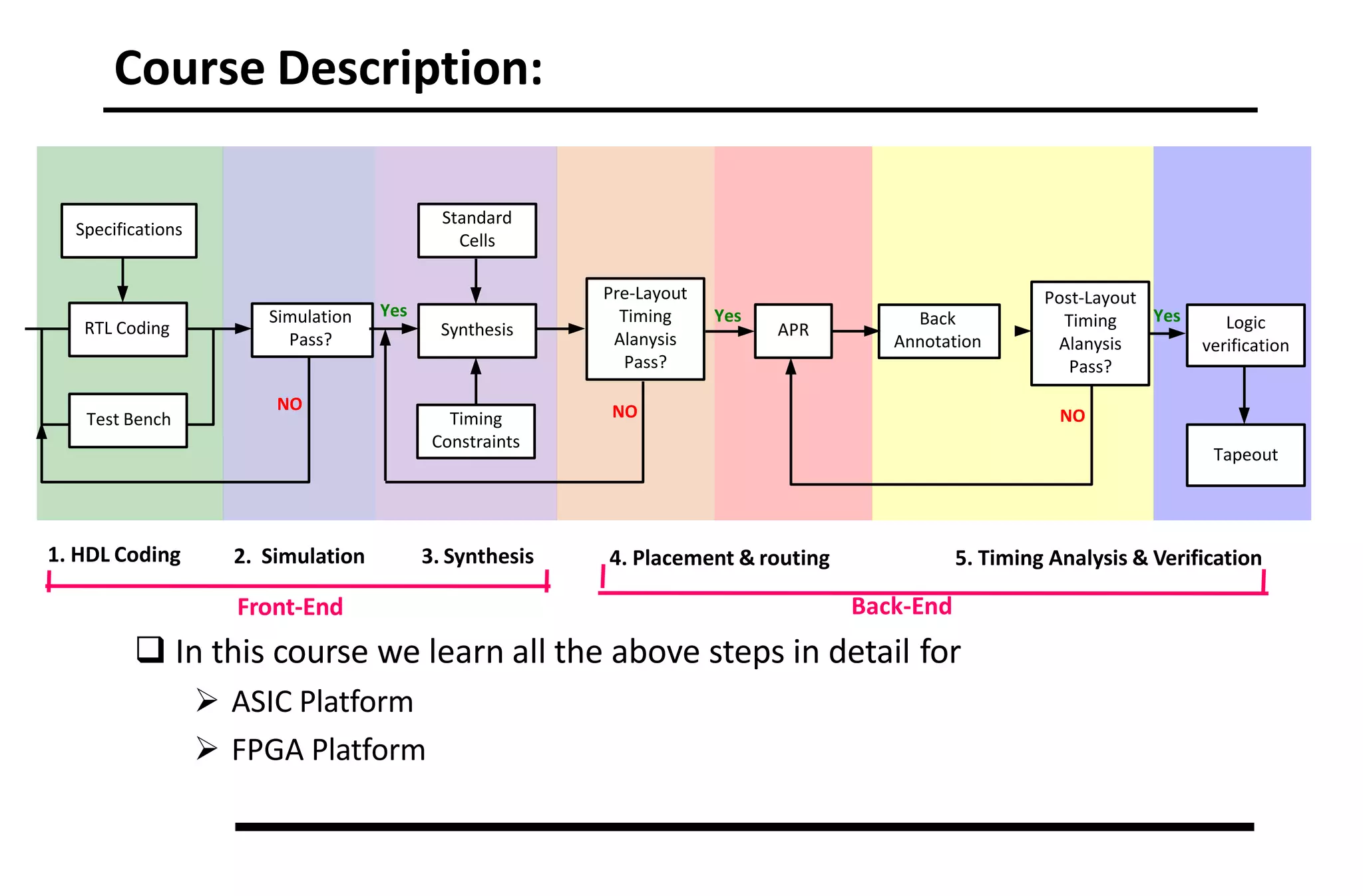
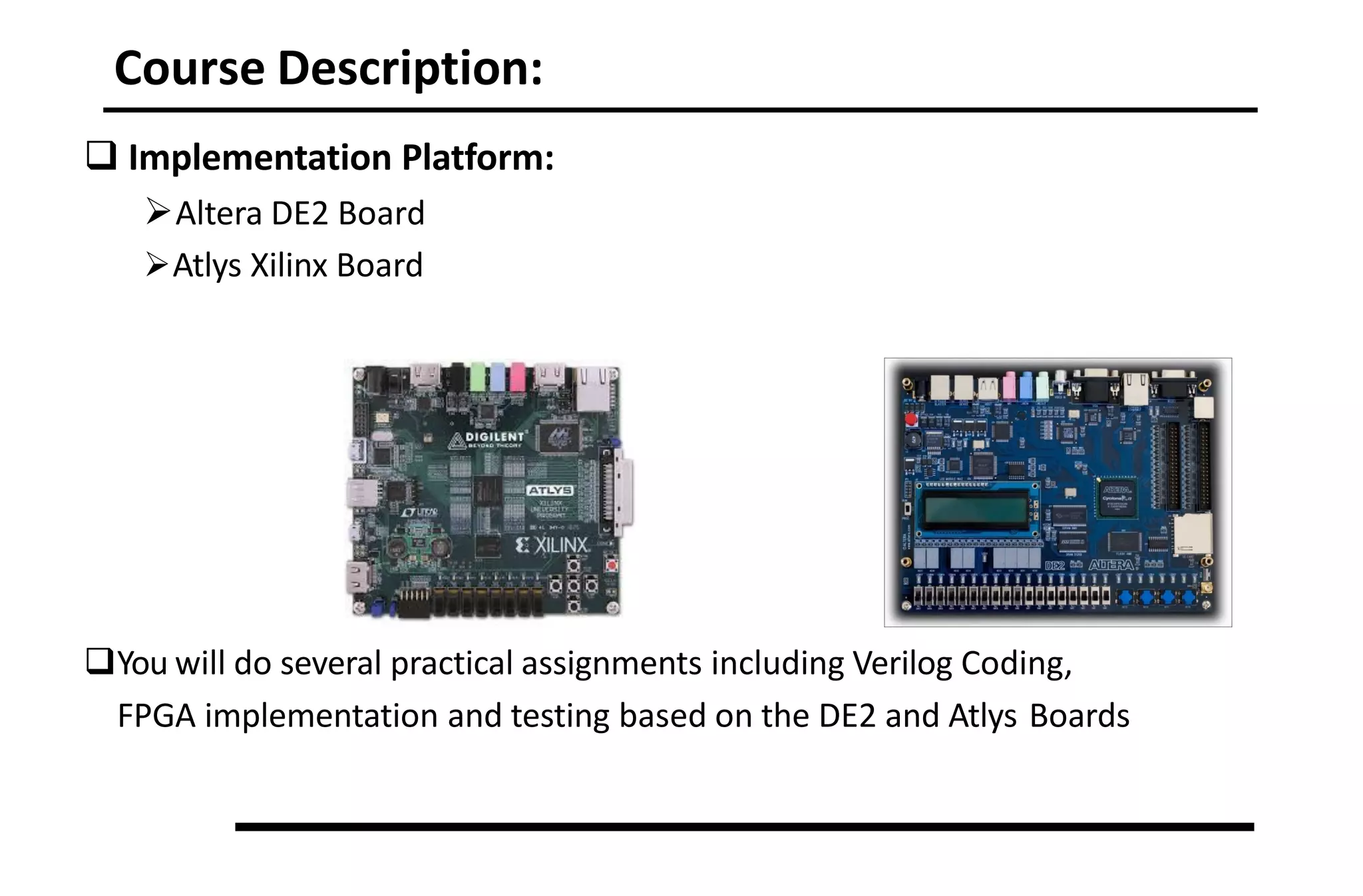
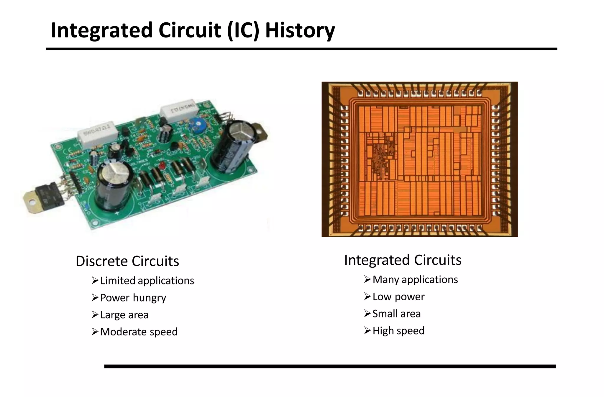
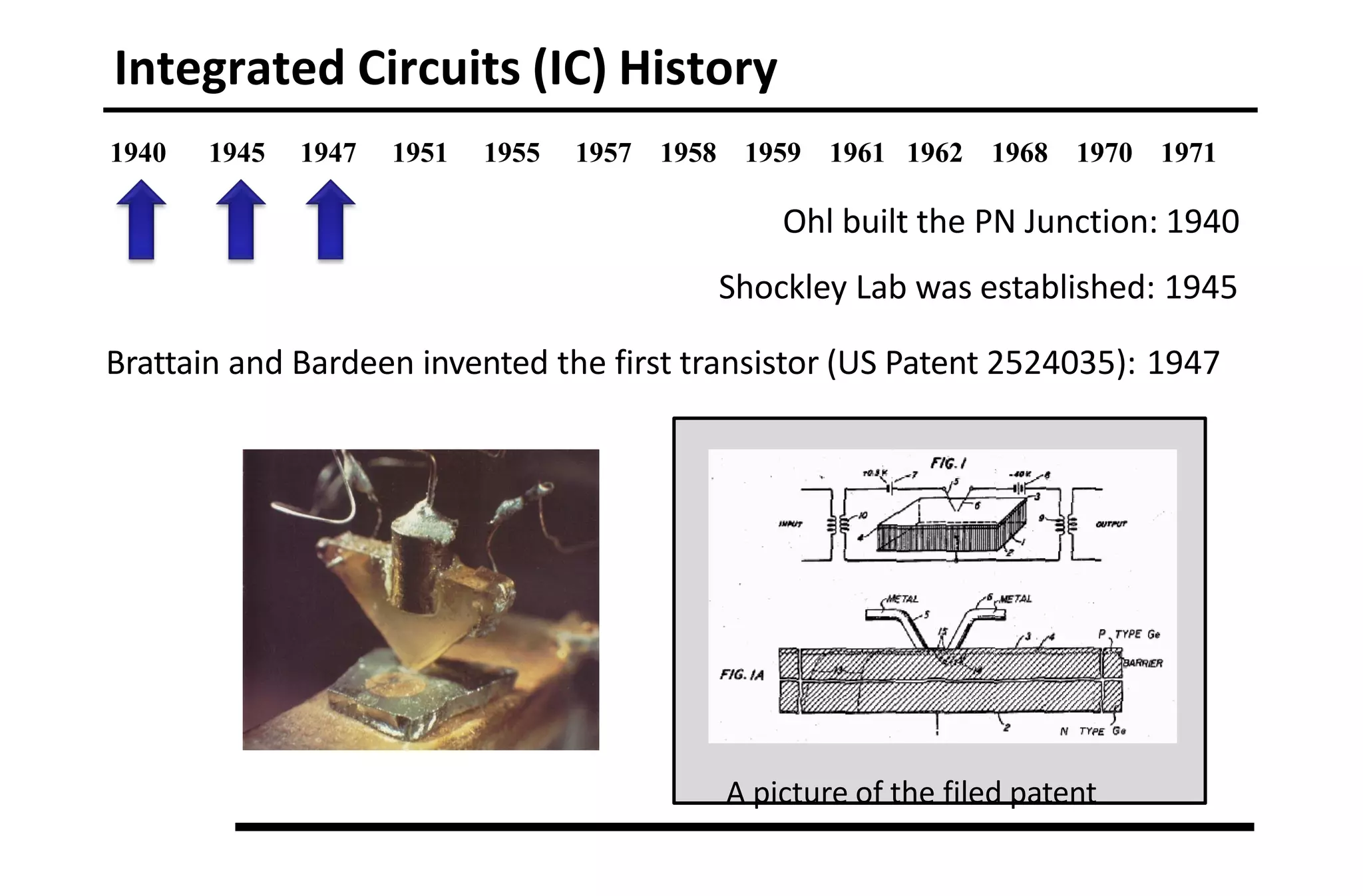
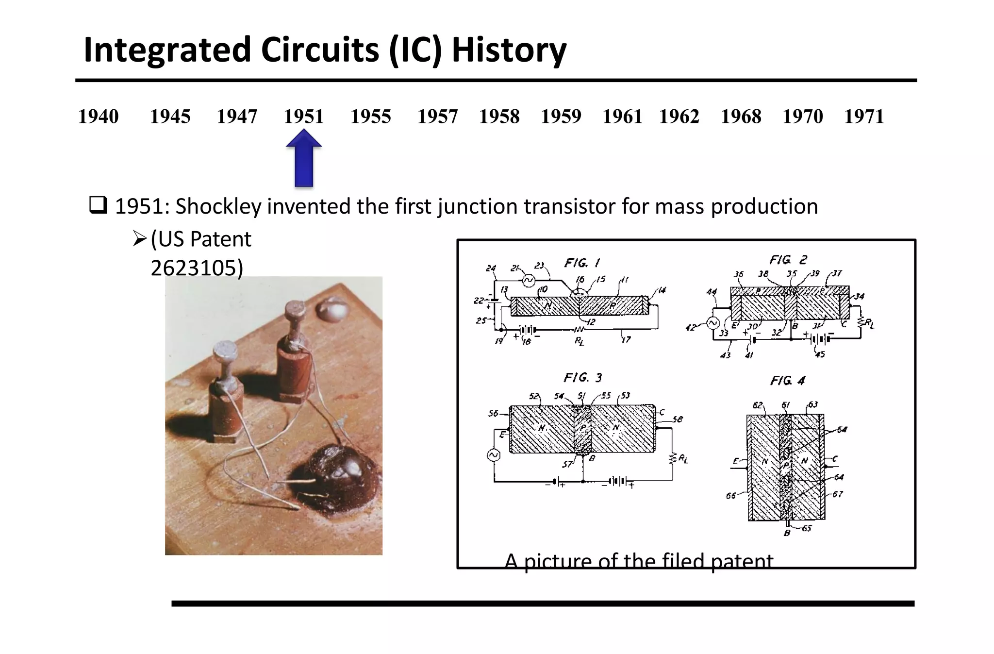
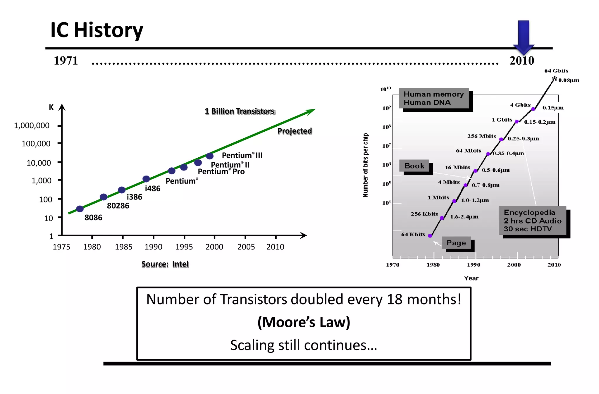
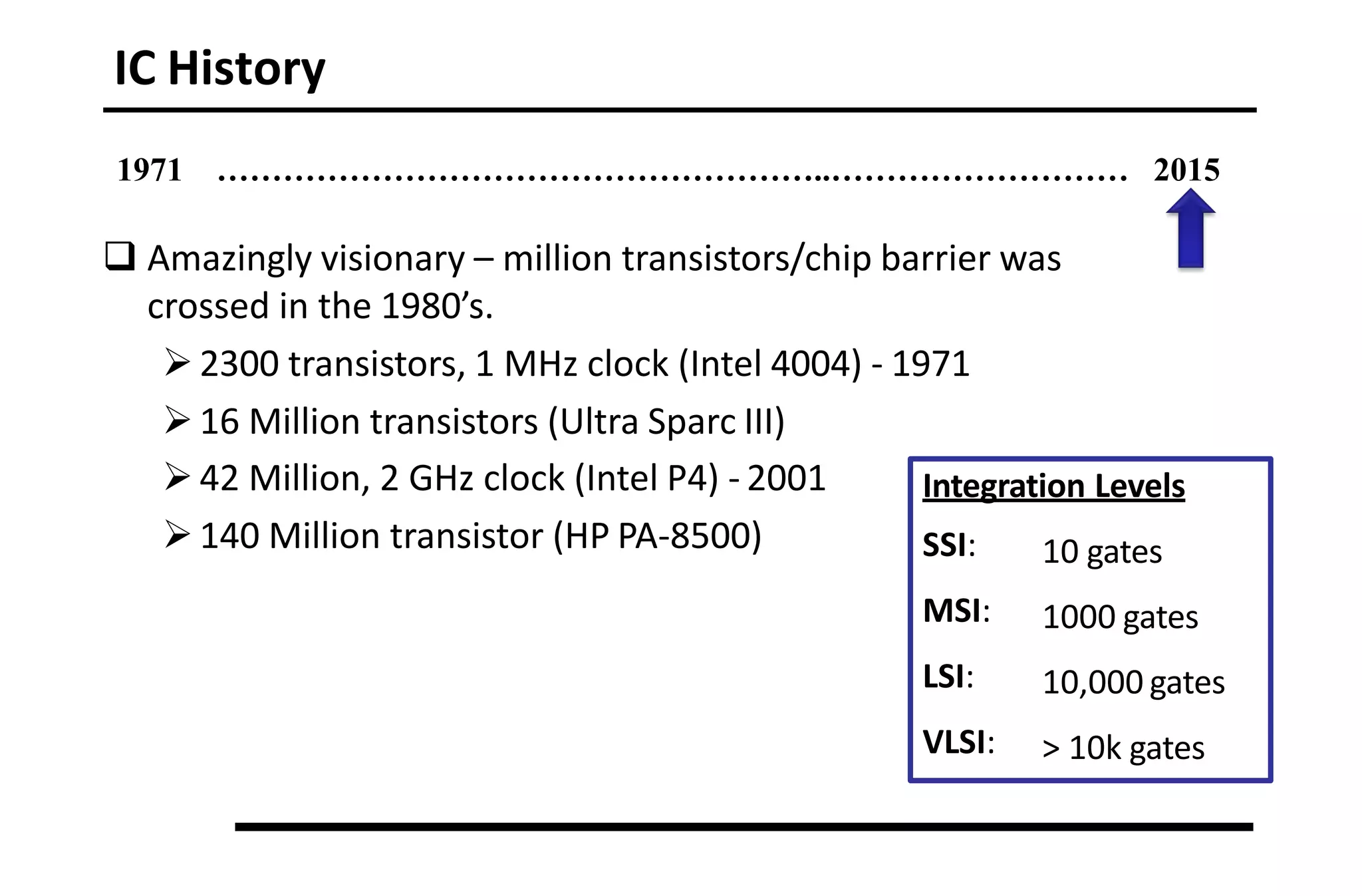
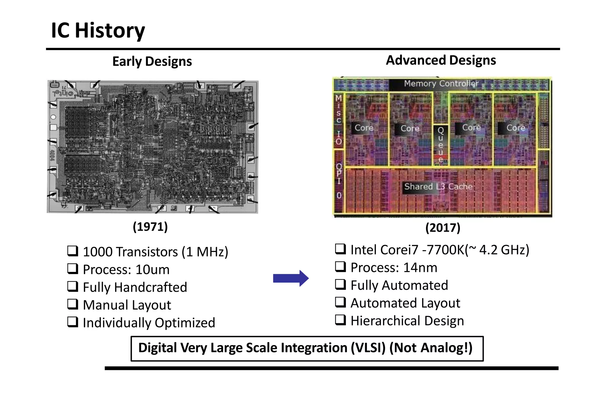
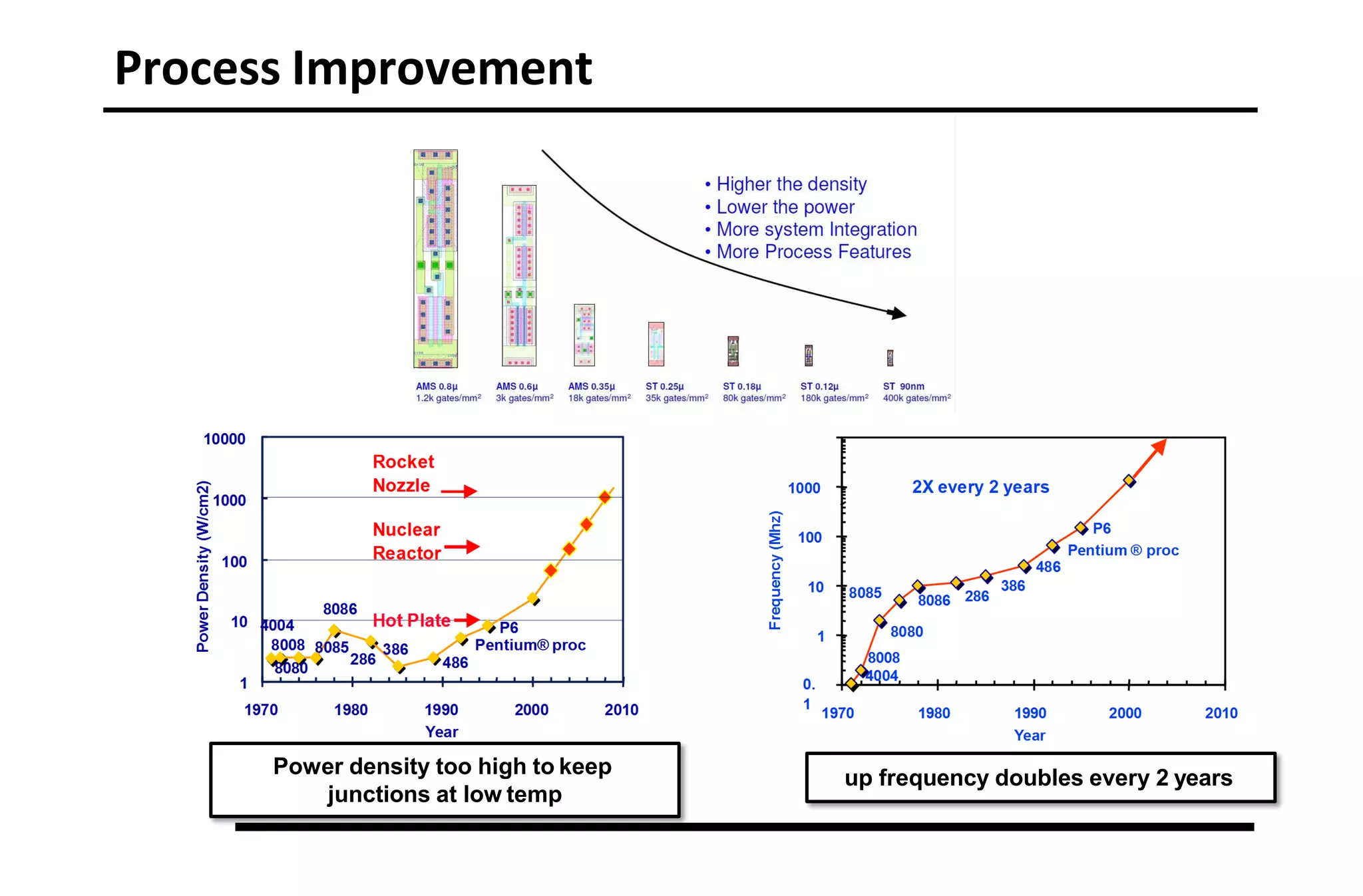
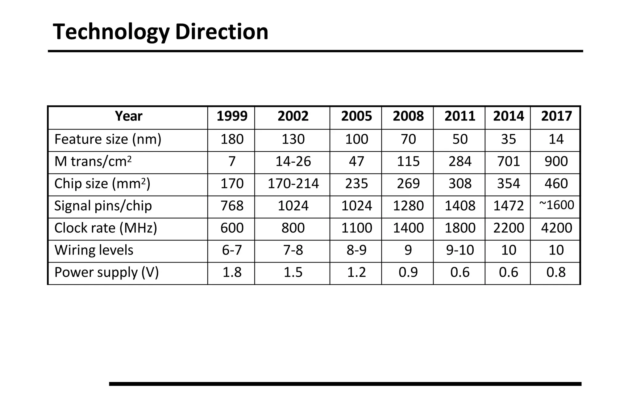
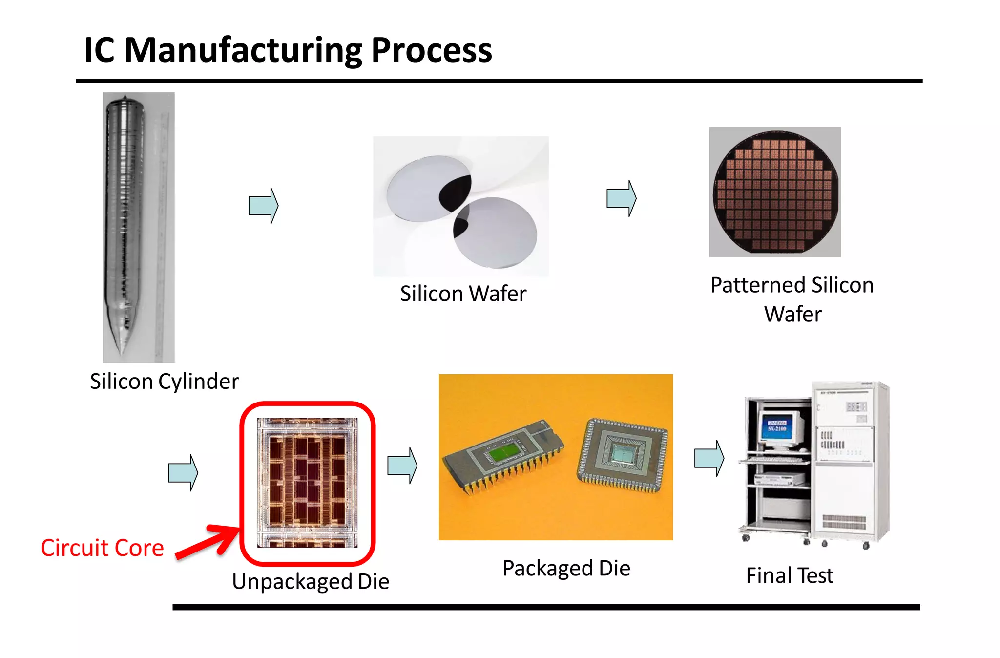
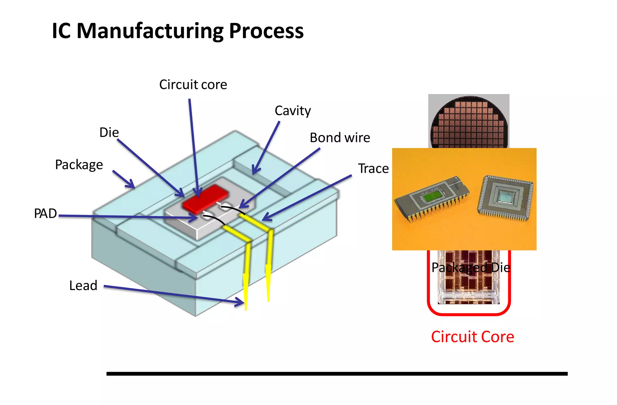
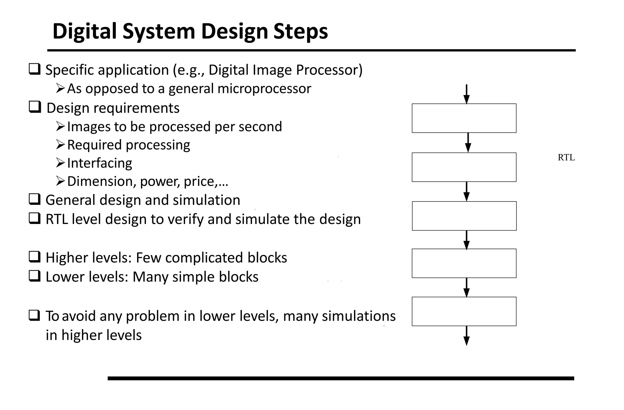
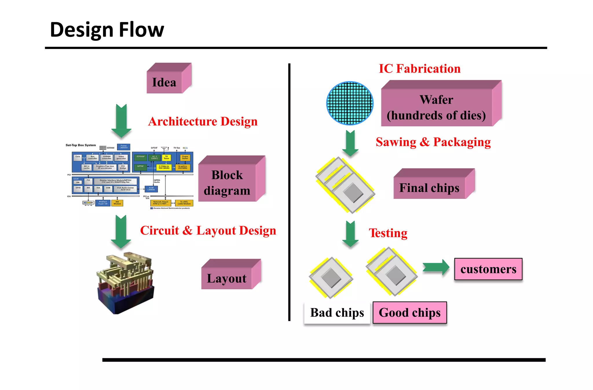
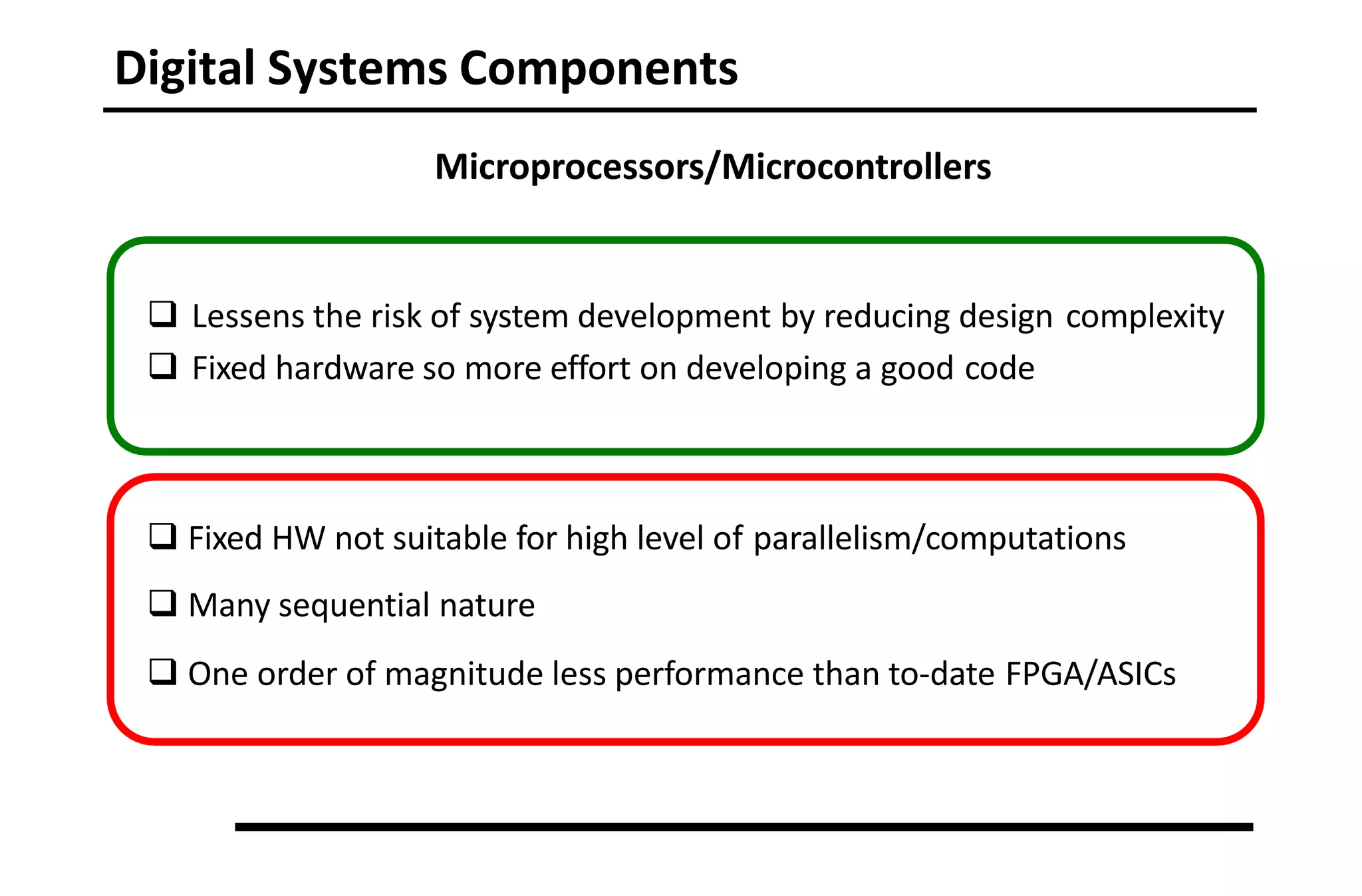
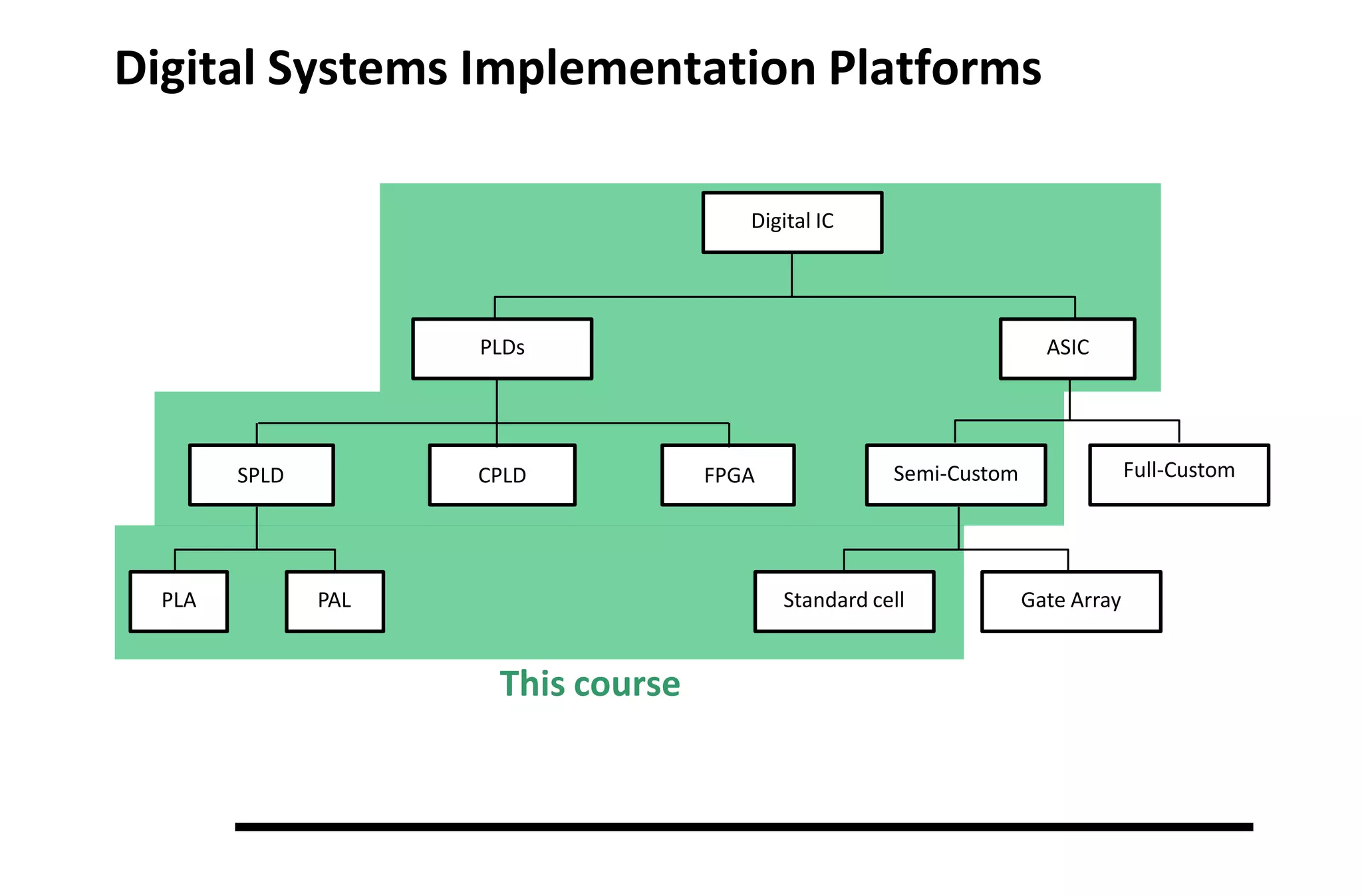
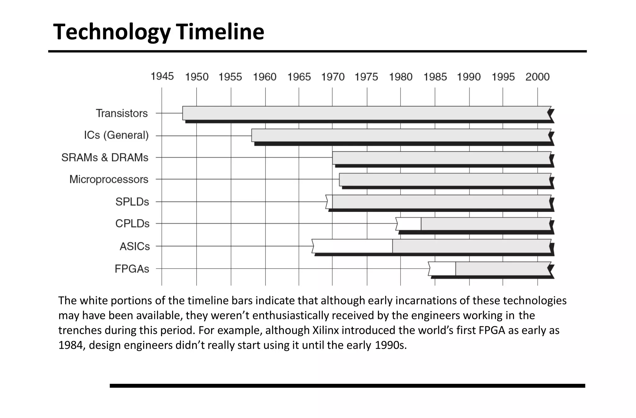
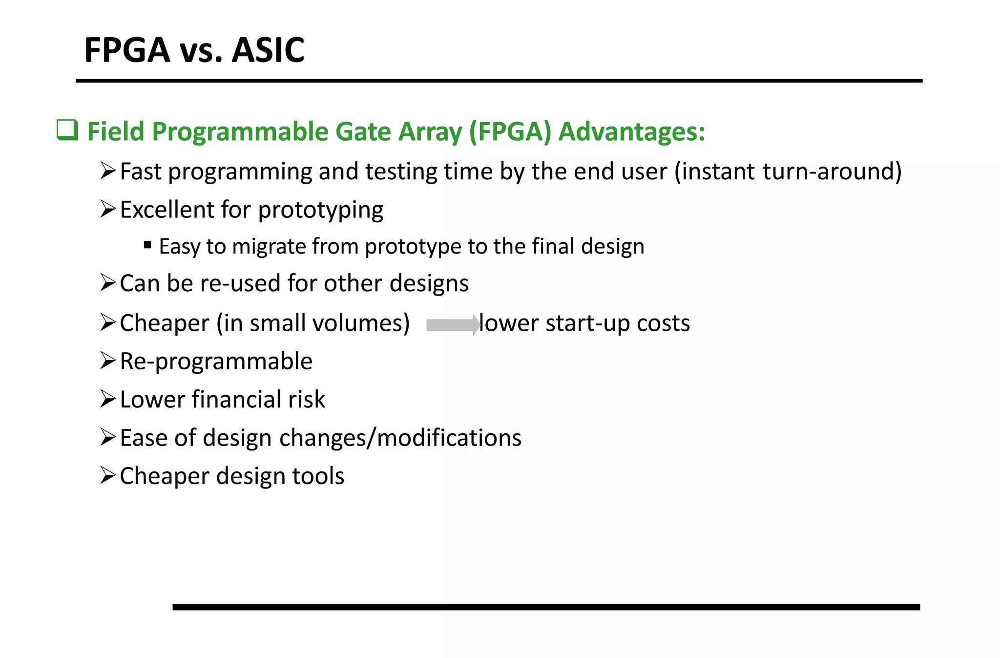
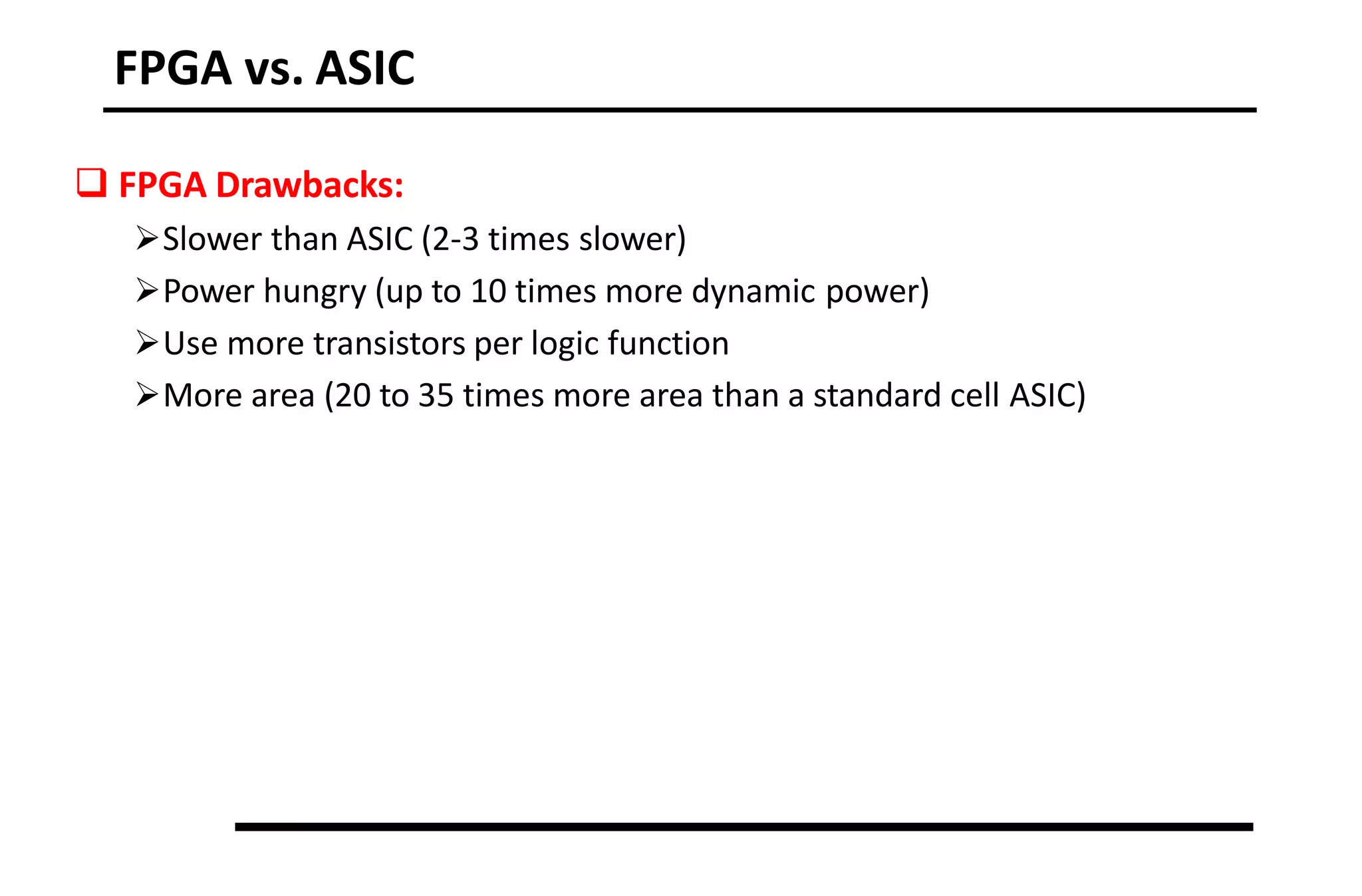
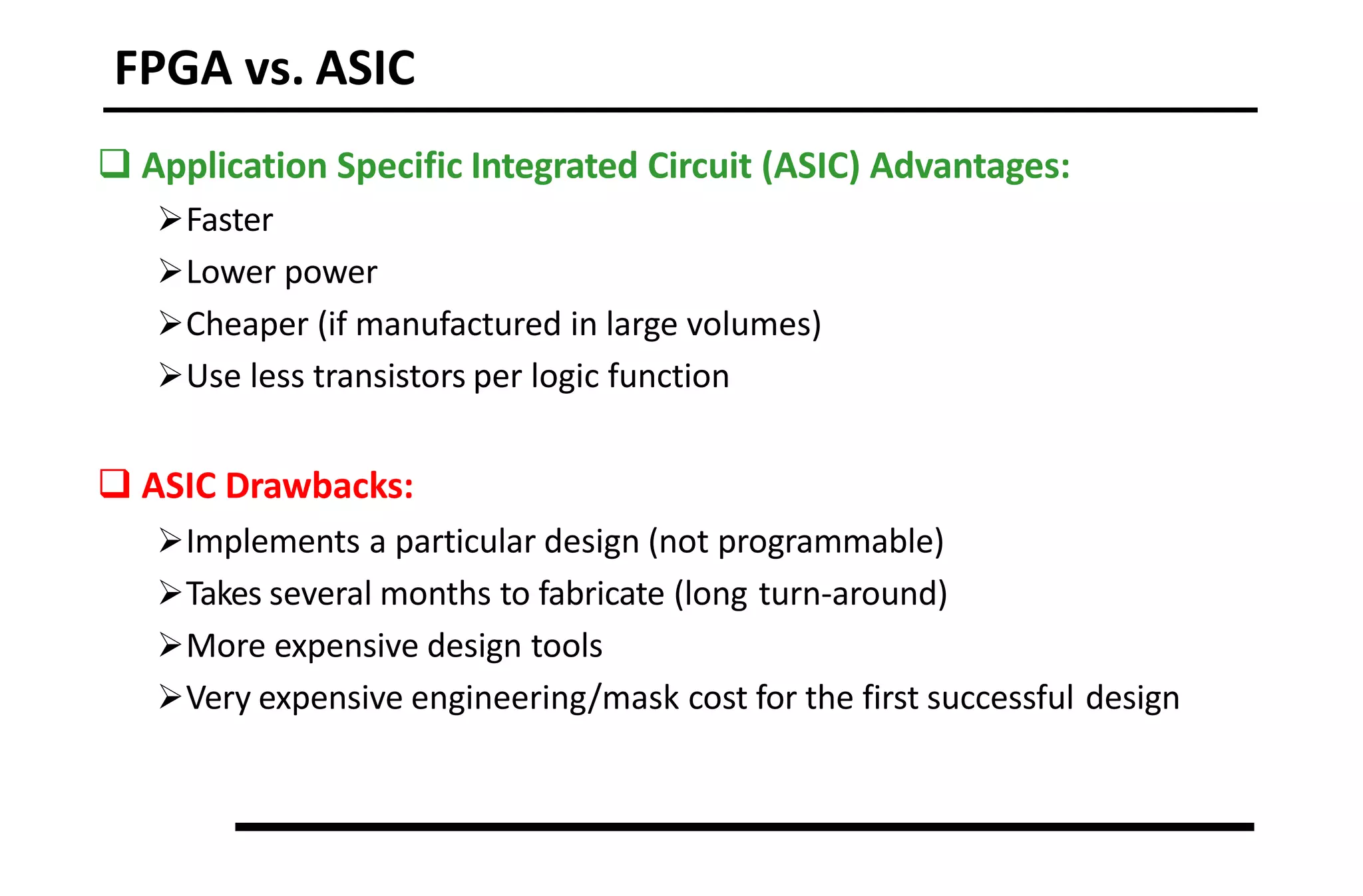
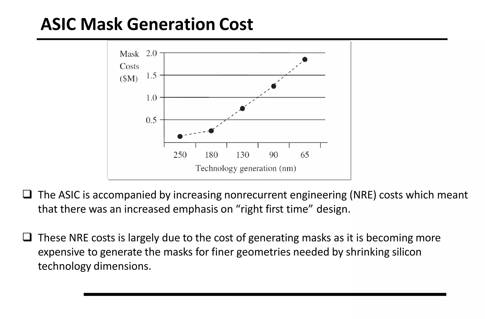
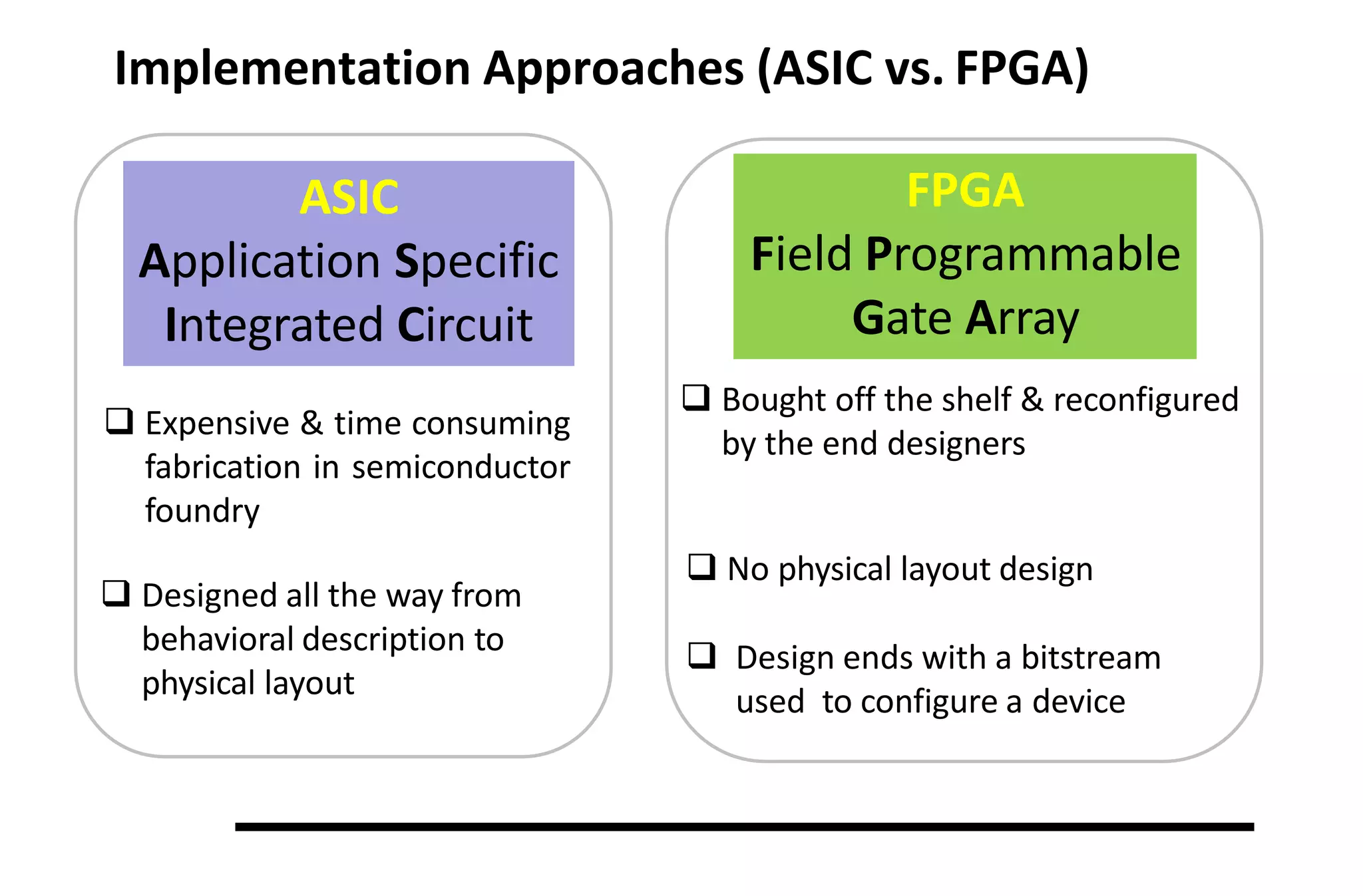
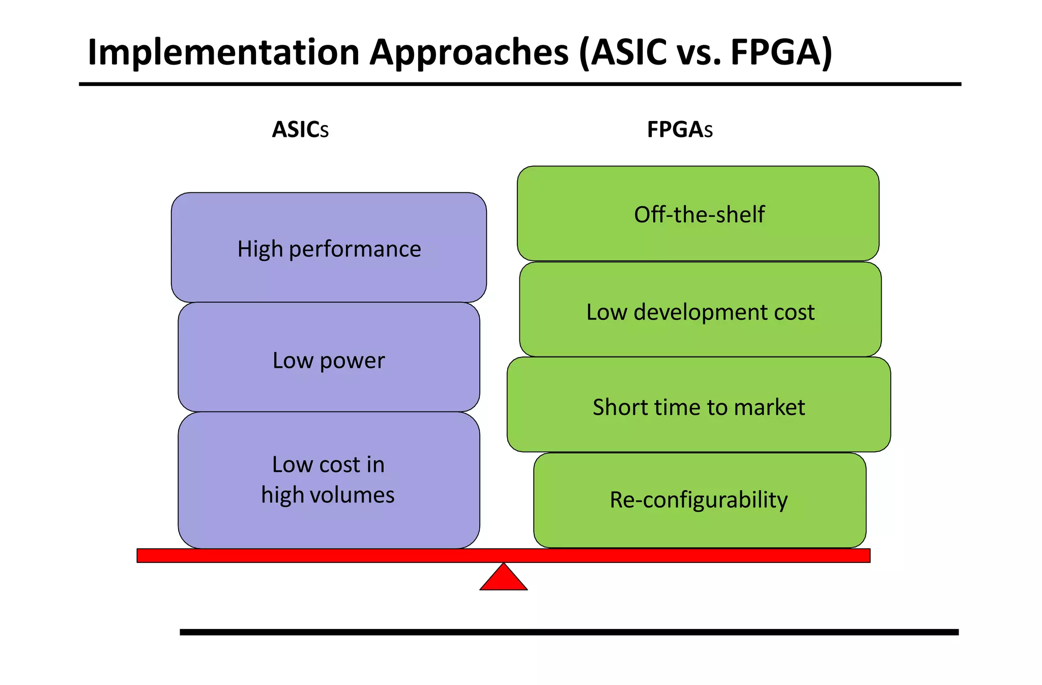
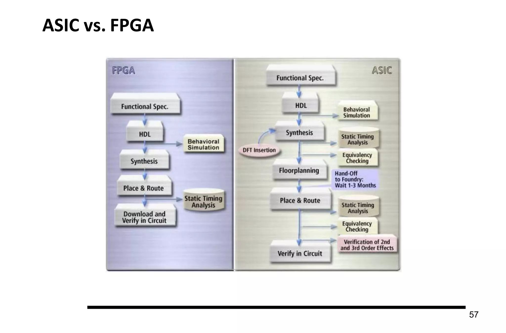
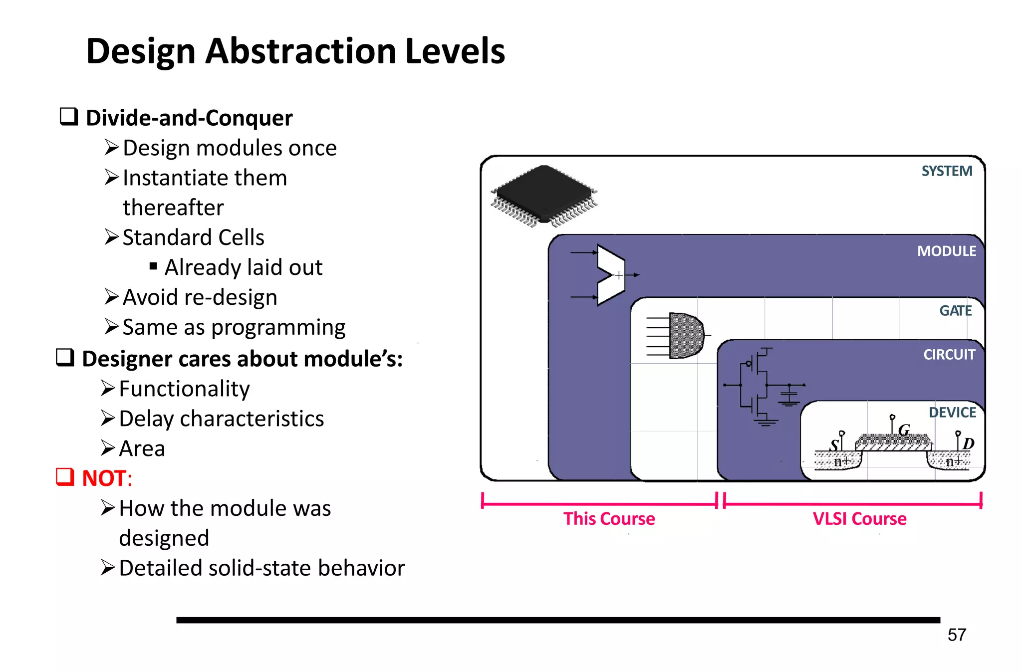
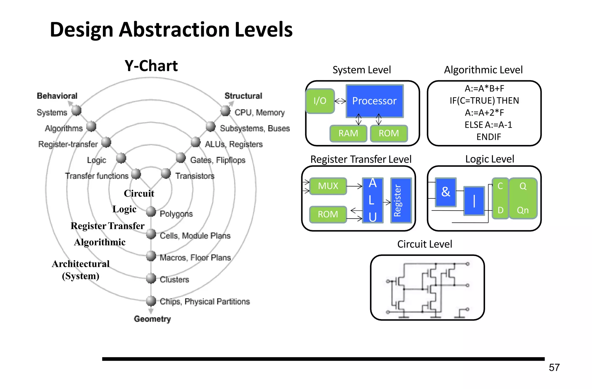
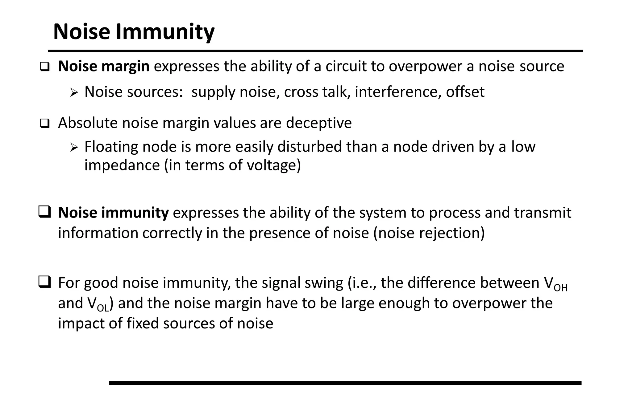
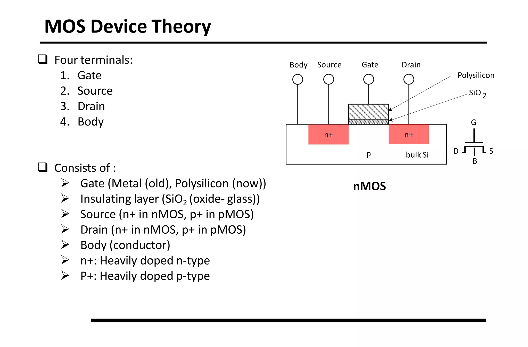
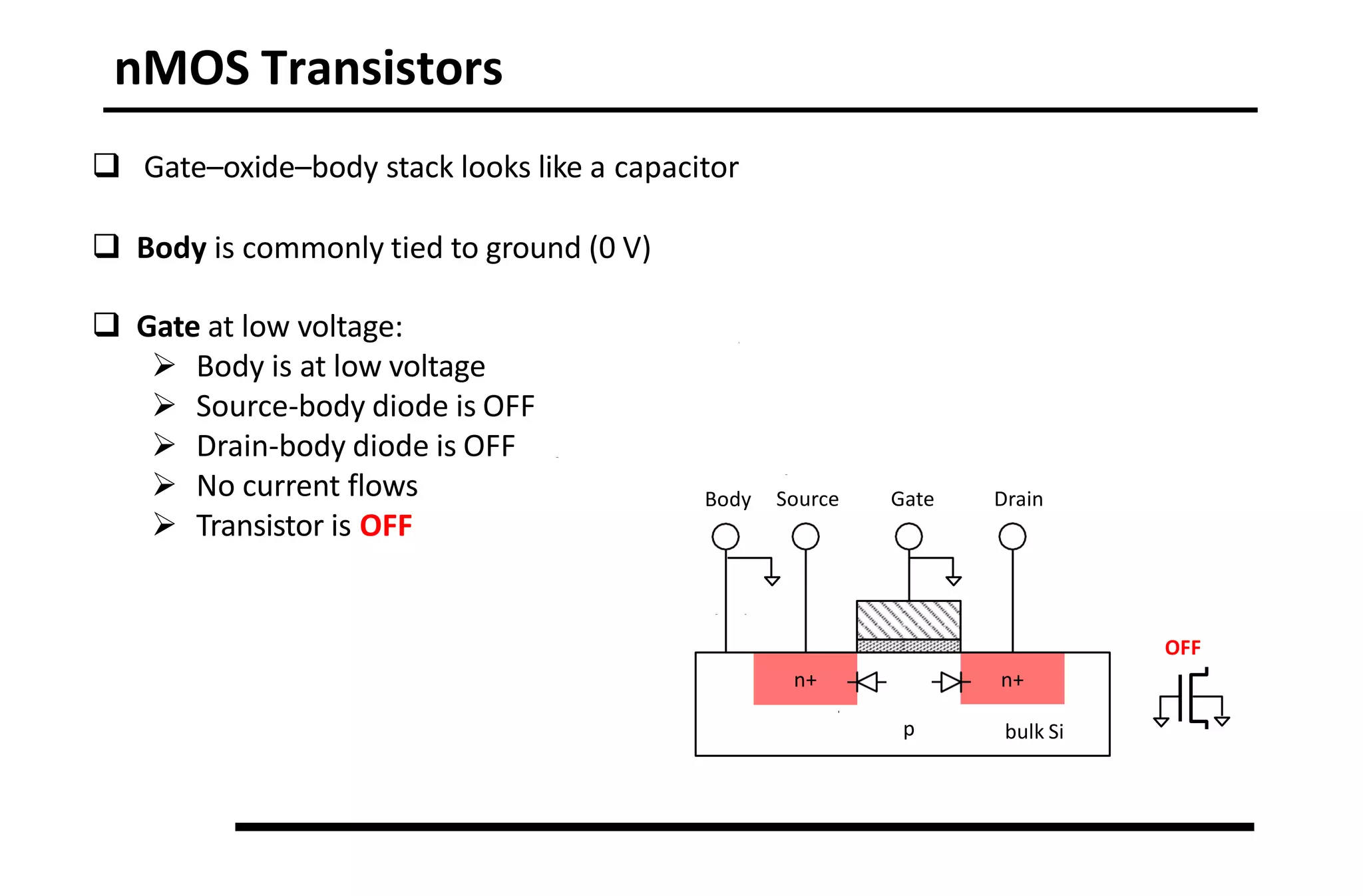
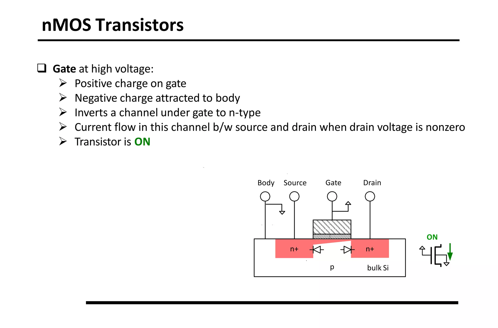
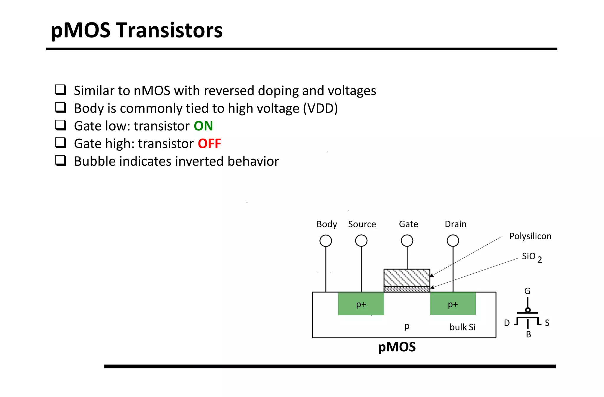
This document outlines a course on FPGA and ASIC design using Verilog. The course is taught by Associate Professor Truong Ngoc Son at the Department of Computer and Communication Engineering. The course covers Verilog coding, simulation, synthesis, FPGA implementation, and the full ASIC design flow. Students will learn design methodologies and use software tools like Xilinx ISE and synthesis tools. The goal is for students to understand the process of taking a design from idea to implementation on FPGAs or as an actual chip.
![Course Description
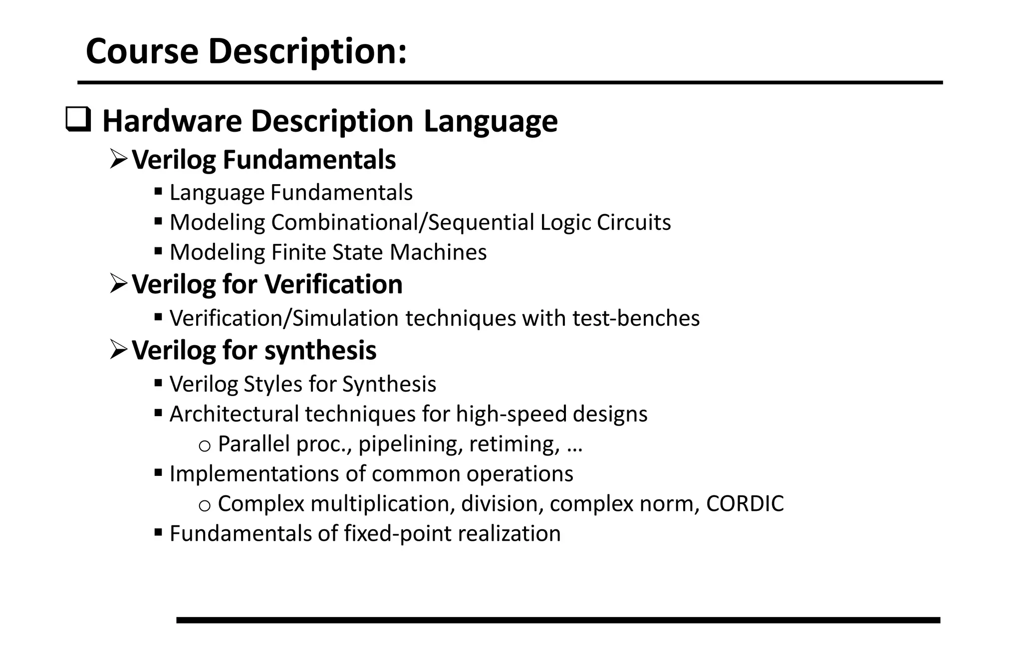
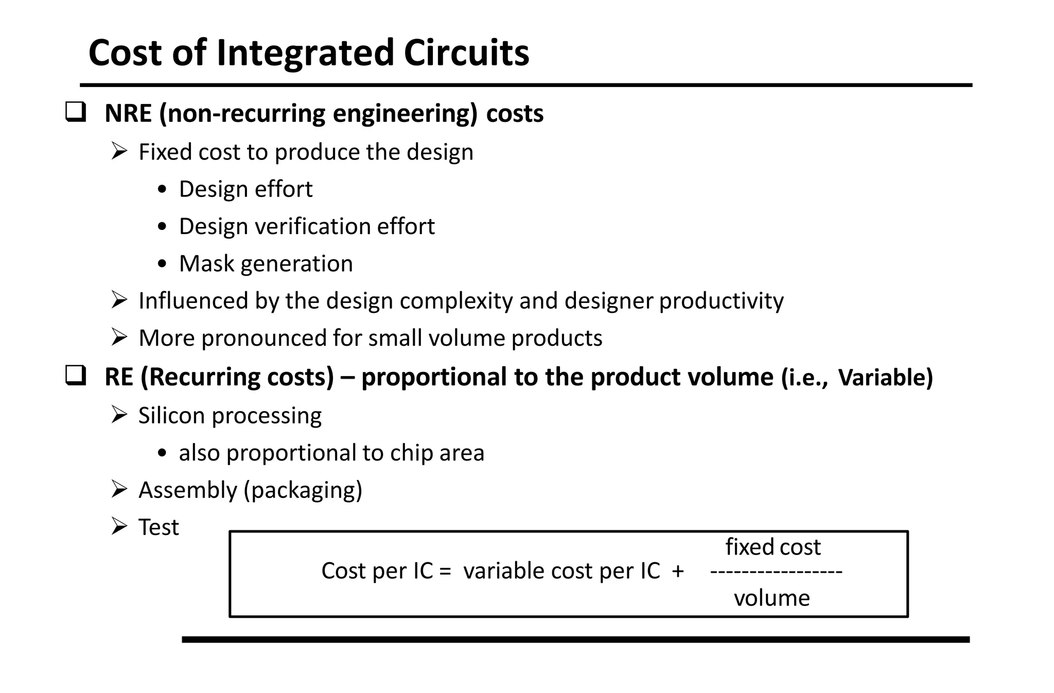
module RippleCarryAdderII (Cin, X, Y,S,Cout);
parameter n = 4; input Cin; input [n-1:0] X, Y; output [n-1:0] S;
wire [n-1:0] C;
Full_Adder stage0 (Cin, X[0], Y[0], S[0], C[1]);
Full_Adder stage1 (C[1], X[1], Y[1], S[1], C[2]);
Full_Adder stage2 (C[2], X[2], Y[2], S[2], C[3]);
Full_Adder stage3 (.Cout(Cout), .Cin(C[3]), .x(X[3]), .y(Y[3]), .S(S[3]));
endmodule
ASIC FPGA
How to go from Idea/Algorithm to the actual hardware](https://image.slidesharecdn.com/chapter01courseintroduction-220828074441-4daa83b7/75/Chapter_01-Course-Introduction-pdf-7-2048.jpg)
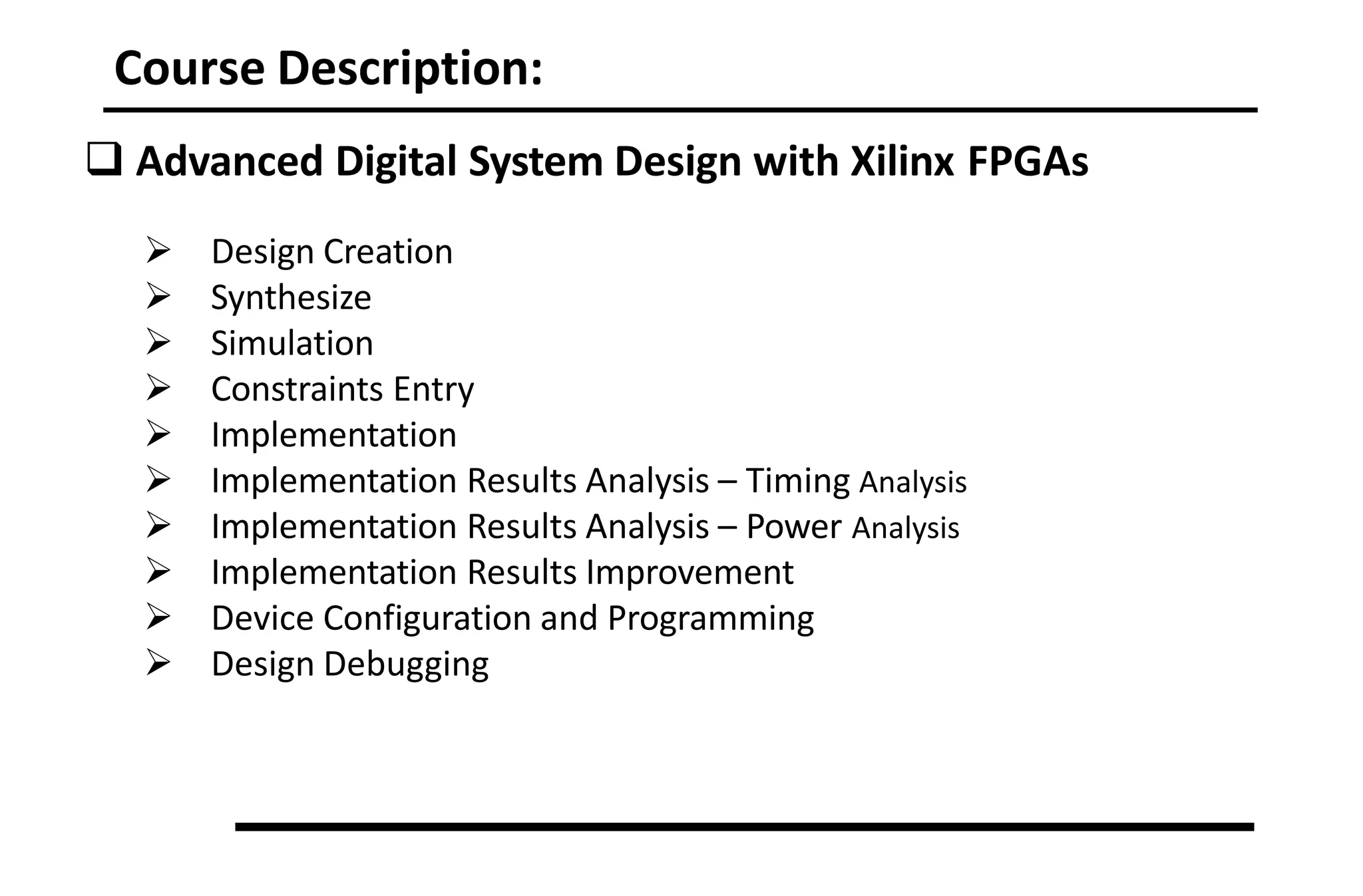
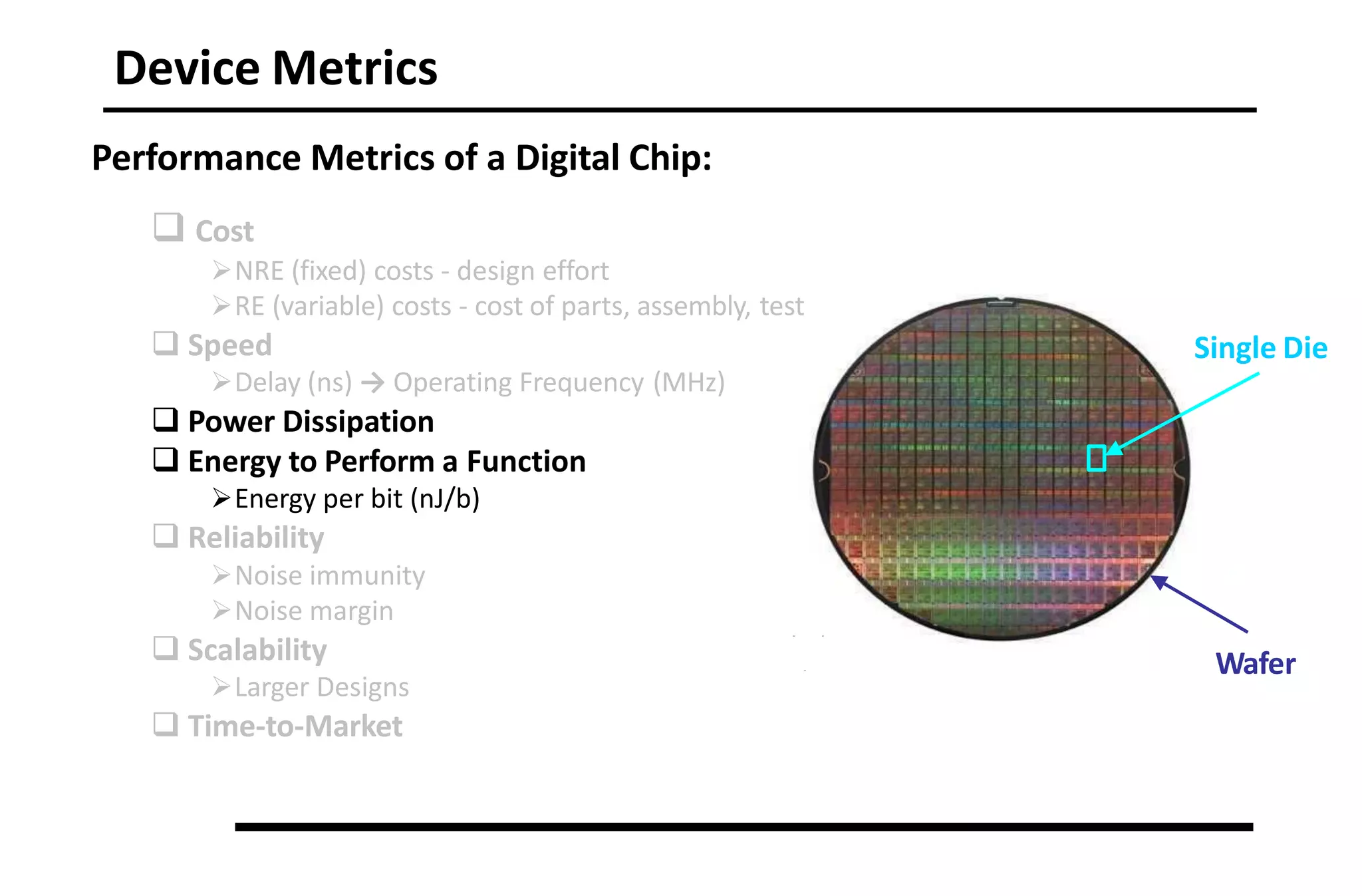
![Power Consumption
Peak transient power
Power line sizing, decoupling, etc.
Average power
Battery current delivery, cooling system
Static power vs. Dynamic power
Static current no computation, etc
Dynamic current Switching on/off the gates
The higher the number of switching events, the higher the dynamic power consumption
Dynamic Energy Amount of energy that is needed to be spent to do a job
Time is no matter
Ppeak = ipeakVsupply =max[p(t)]](https://image.slidesharecdn.com/chapter01courseintroduction-220828074441-4daa83b7/75/Chapter_01-Course-Introduction-pdf-66-2048.jpg)


![Vibe Coding vs. Spec-Driven Development [Free Meetup]](https://cdn.slidesharecdn.com/ss_thumbnails/vibecodingvsspecdrivendevelopment-251209105622-43f455e7-thumbnail.jpg?width=640&height=640&fit=bounds)


