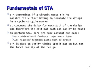
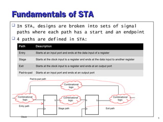
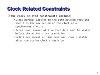
Static timing analysis (STA) determines if a circuit meets timing constraints without simulation. It computes delays for each path, finding critical paths. STA assumes no combinational feedback loops and broken register feedback paths. Paths include entry, stage, exit, and pad-to-pad. Timing constraints include clock period, setup time, hold time, input delay, output delay, and input-output delay. STA is used to verify timing but not functionality.


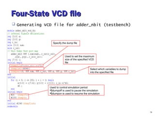
![Four-State VCD fileFour-State VCD file
VCD file format:
20
$date
Fri Sep 05 17:32:13 2014
$end
$version
ModelSim Version 10.1c
$end
$timescale
1ps
$end
$scope module adder_nbit_vcd_tb $end
$scope module UUT $end
$var wire 1 ! sum [3] $end
$var wire 1 " sum [2] $end
$var wire 1 # sum [1] $end
$var wire 1 $ sum [0] $end
$var wire 1 % c_out $end
$var wire 1 & x [3] $end
$var wire 1 ' x [2] $end
$var wire 1 ( x [1] $end
$var wire 1 ) x [0] $end
$var wire 1 * y [3] $end
$var wire 1 + y [2] $end
$var wire 1 , y [1] $end
$var wire 1 - y [0] $end
$var wire 1 . c_in $end
$upscope $end
$upscope $end
$enddefinitions $end
#0
$dumpvars
0$
0#
0"
0!
0%
0.
0)
0(
0'
0&
0-
0,
0+
0*
$end
#5000
1-
1$
#10000
0-
1,
0$
1#
#15000
1-
1$
#20000
$dumpoff
x$
x#
x"
x!
x%
x.
x)
x(
x'
x&
x-
x,
x+
x*
$end](https://image.slidesharecdn.com/verification-141009053122-conversion-gate01/85/Verilog-HDL-Verification-20-320.jpg)


![[Back2School] Constraint Develop.pdf- Chapter 3](https://cdn.slidesharecdn.com/ss_thumbnails/constraintdevelop-250606153235-d8296a49-thumbnail.jpg?width=640&height=640&fit=bounds)


![[Back2School] STA Basic Concepts- Chapter 1.pdf](https://cdn.slidesharecdn.com/ss_thumbnails/stabasicconcepts-250524204554-25ac4895-thumbnail.jpg?width=640&height=640&fit=bounds)