Download as PDF, PPTX
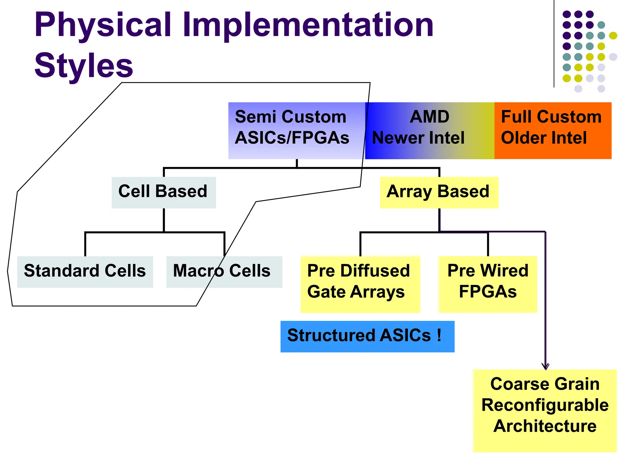
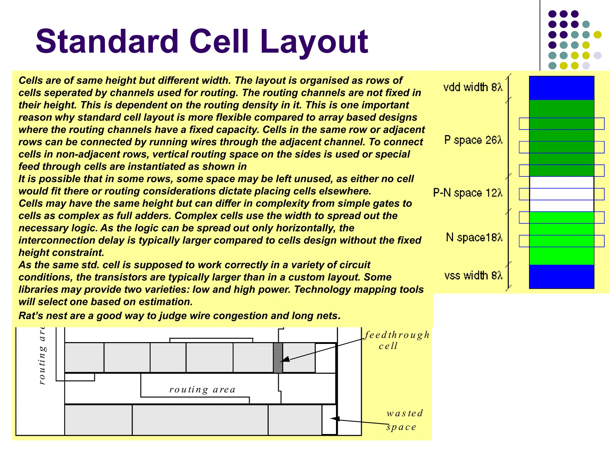
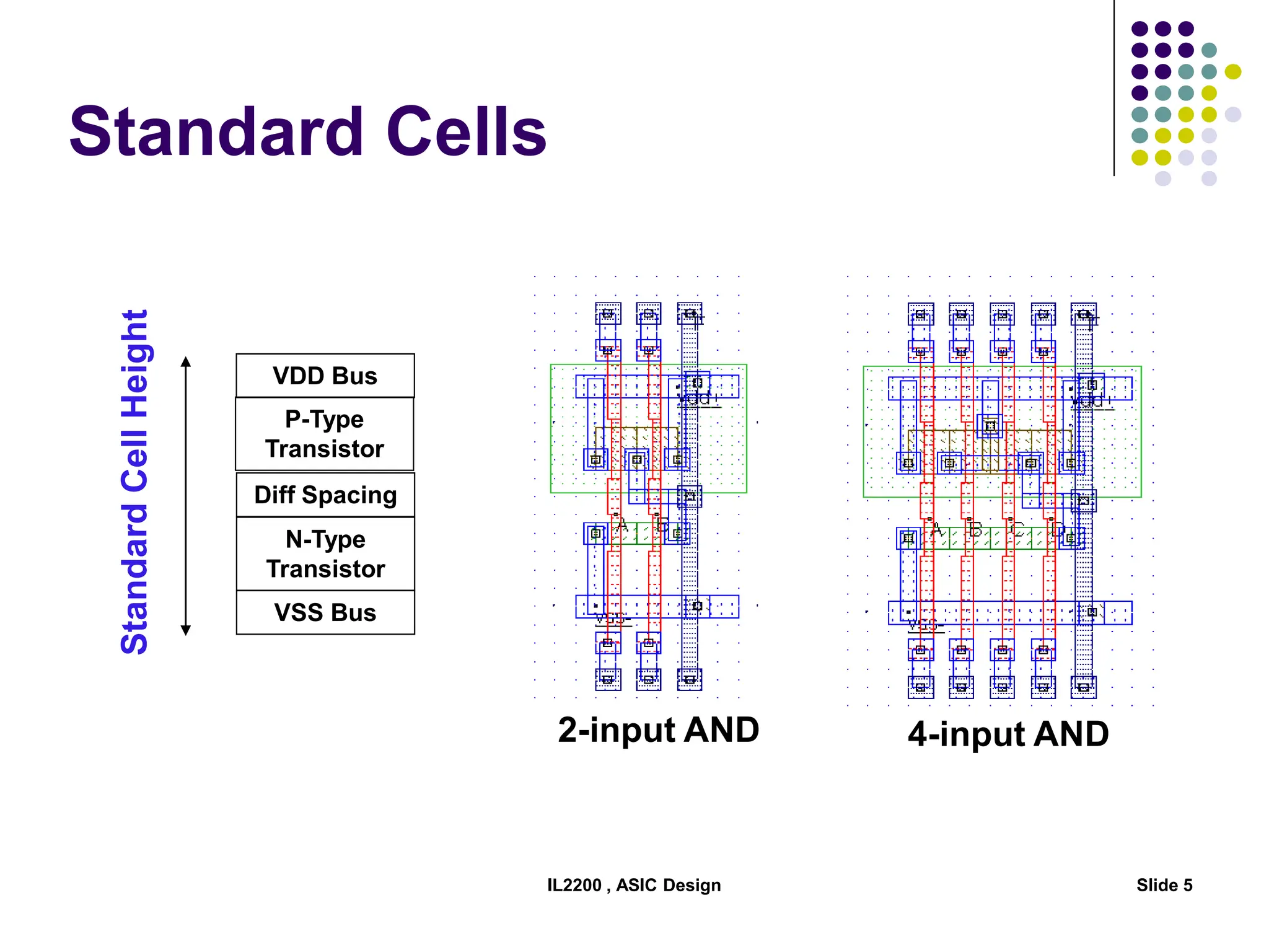
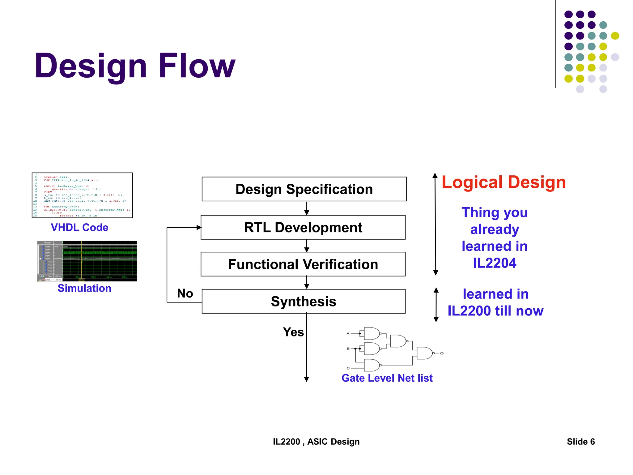
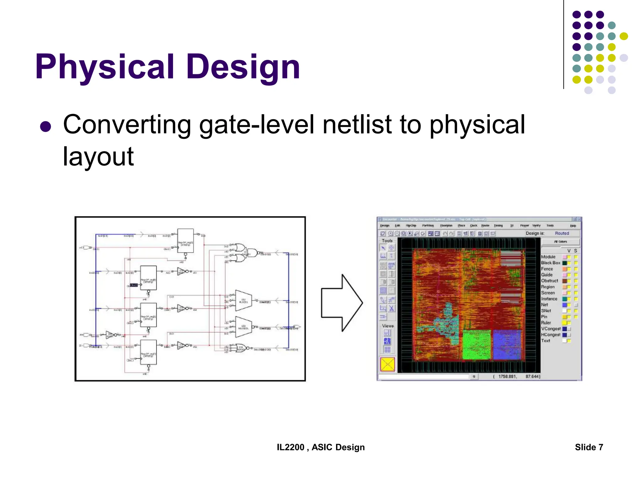
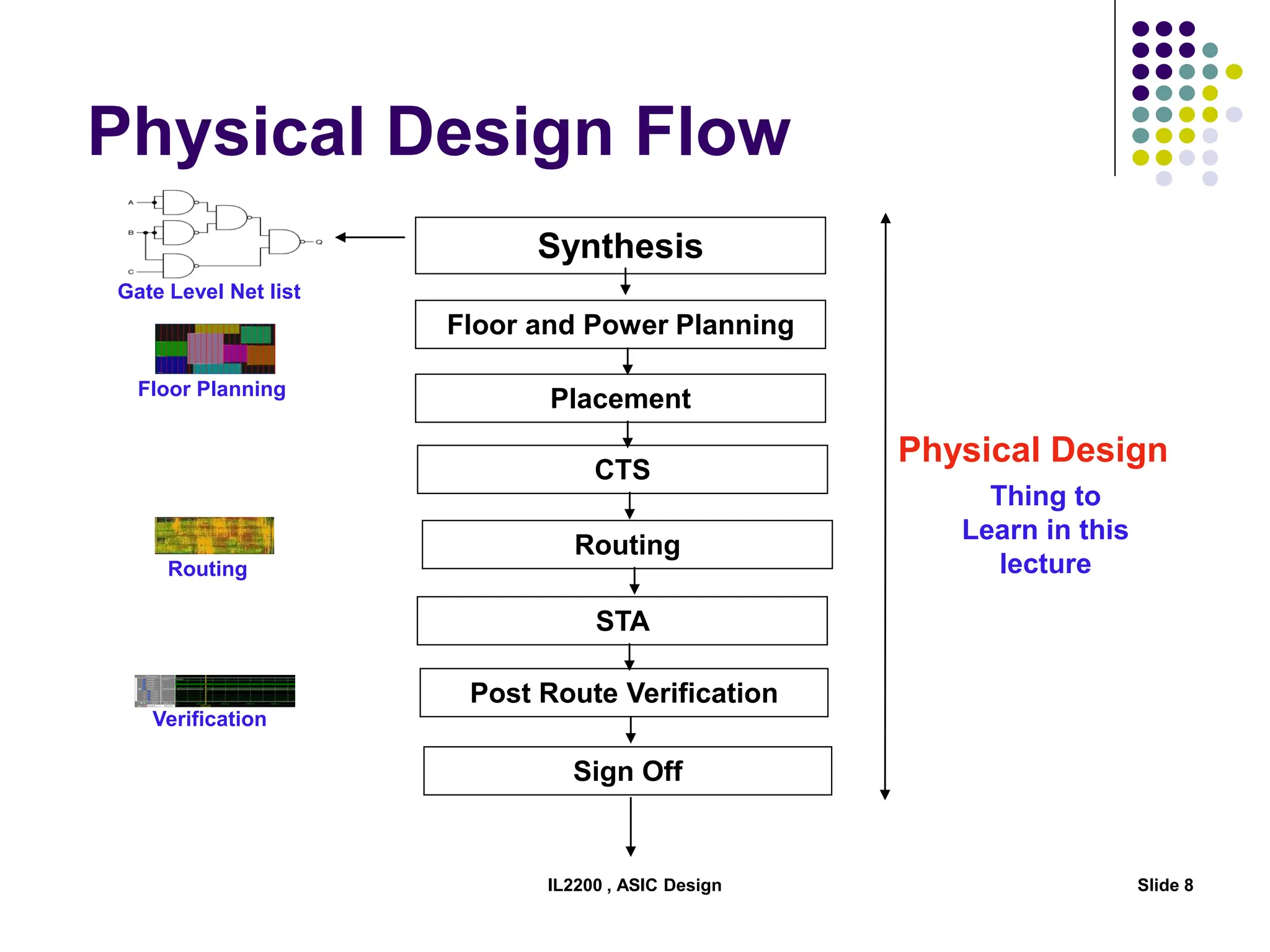
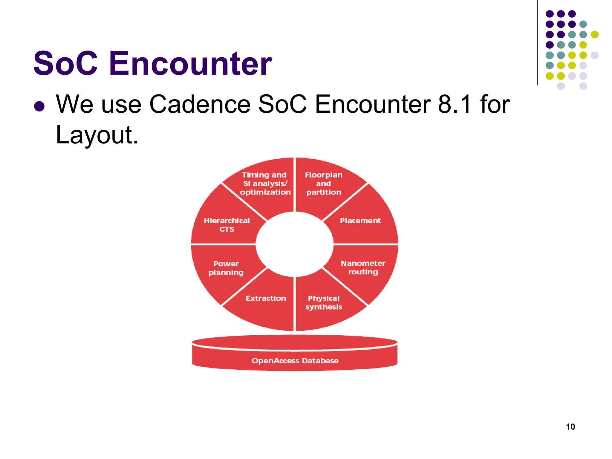
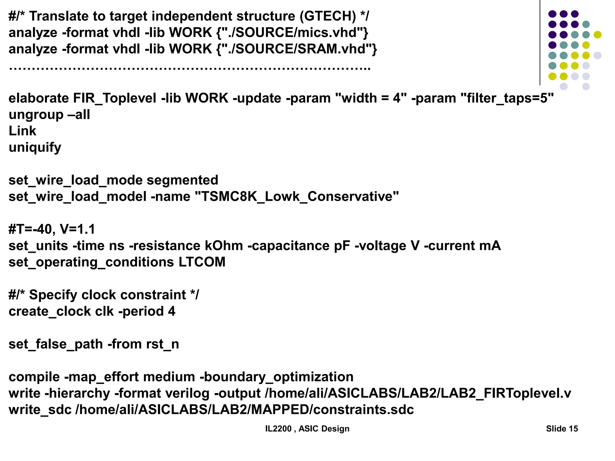
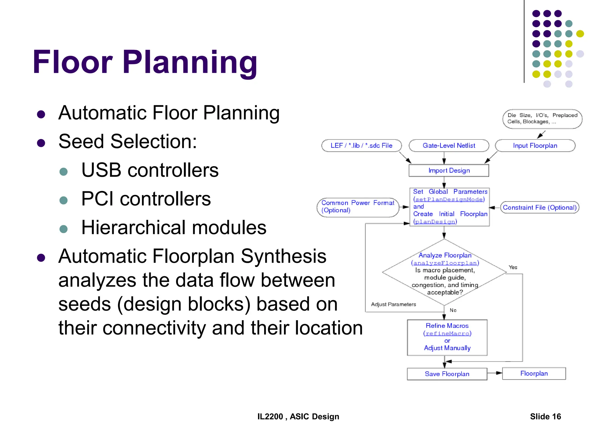
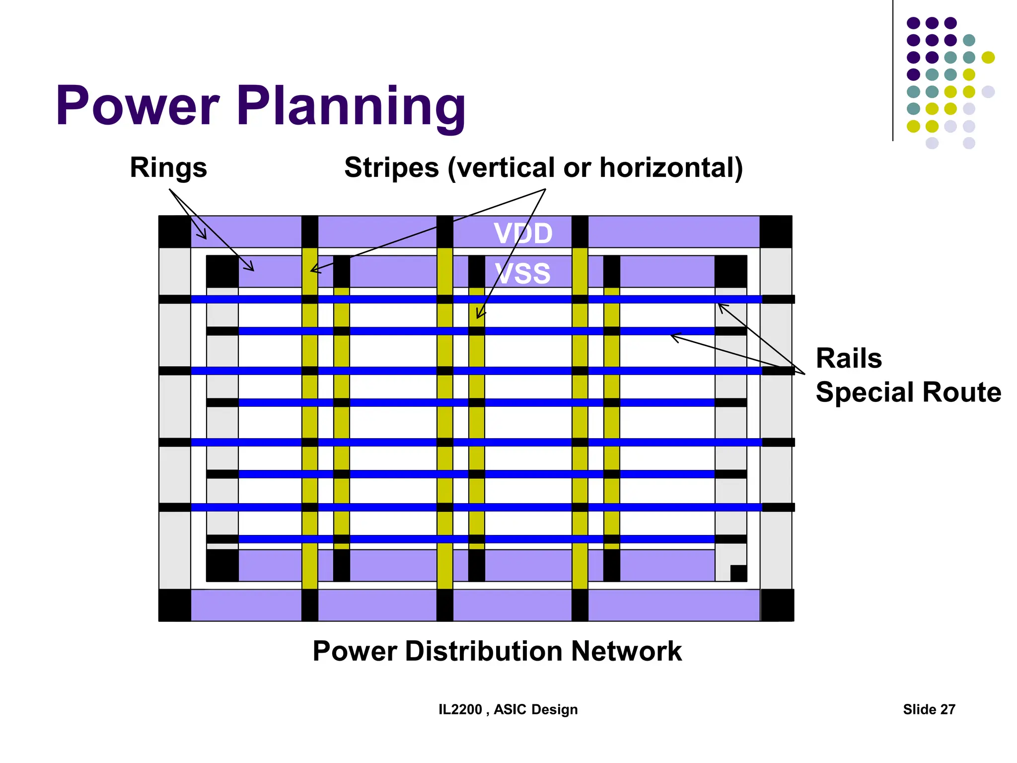
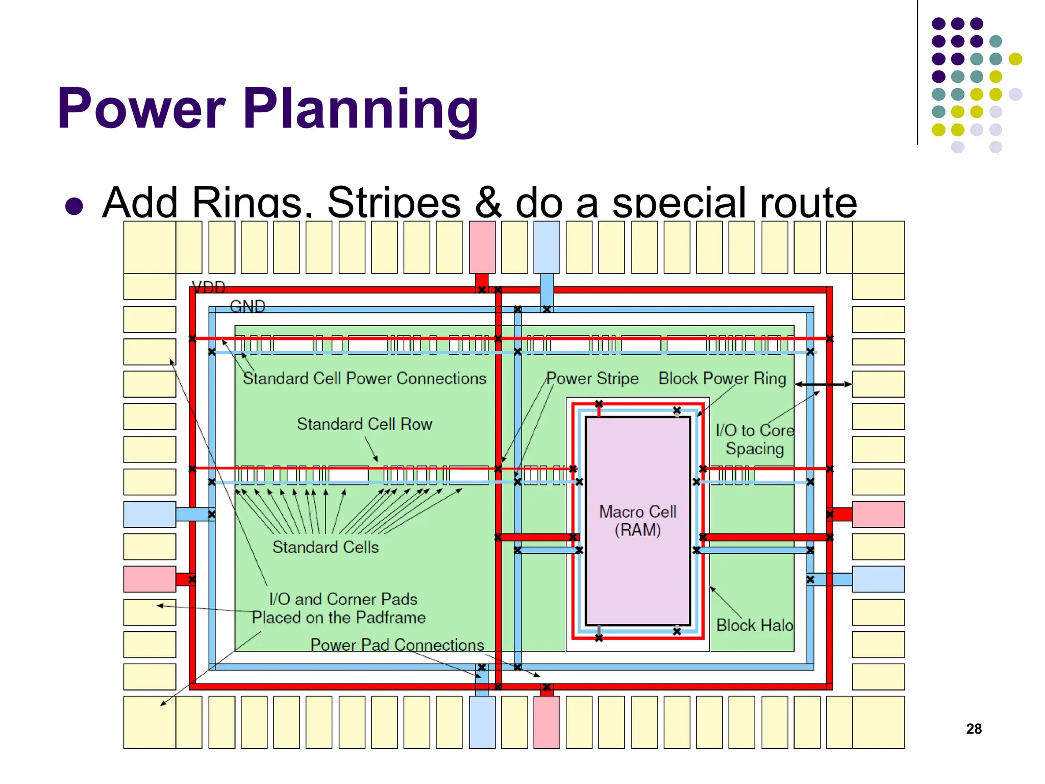
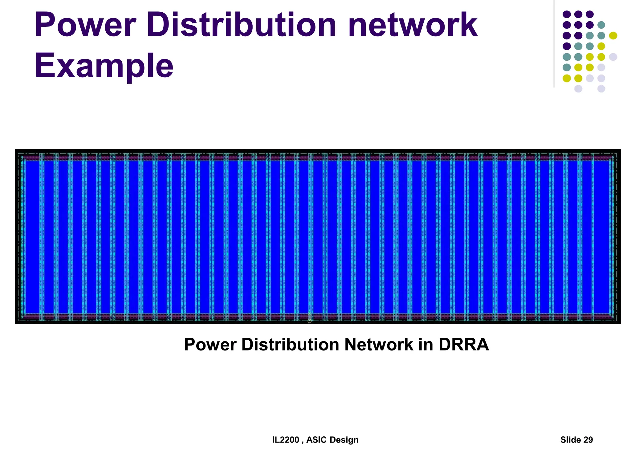

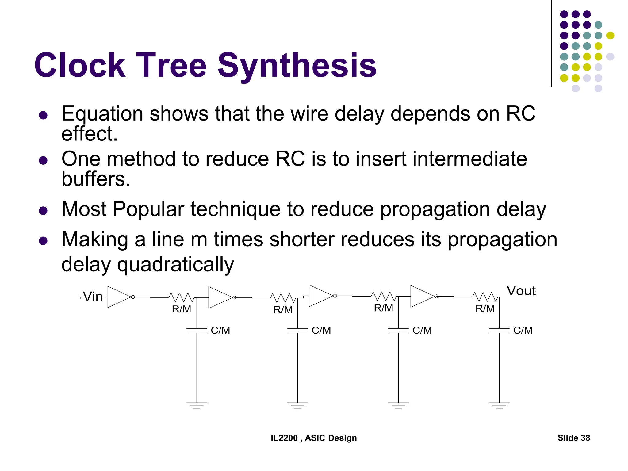
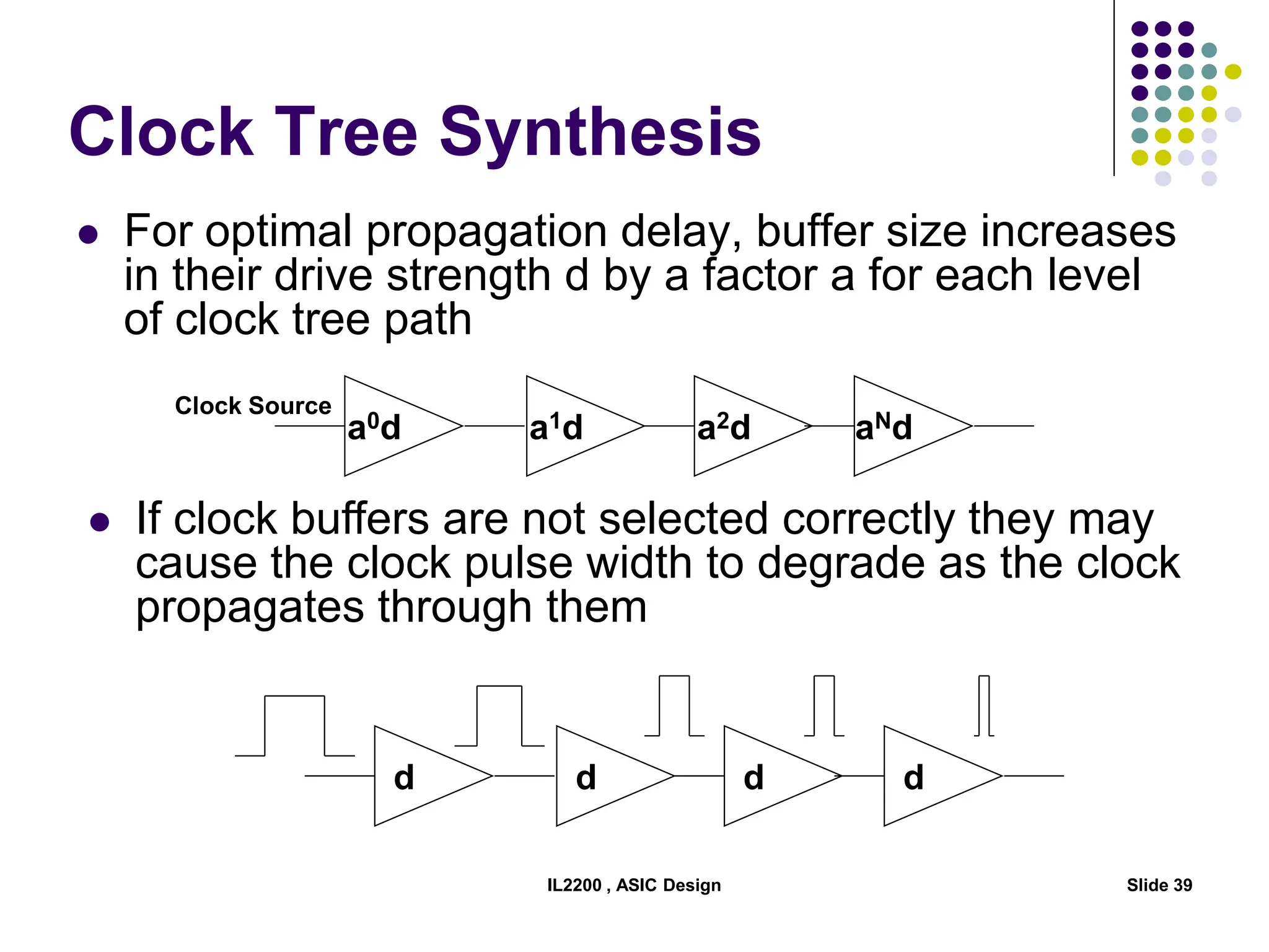
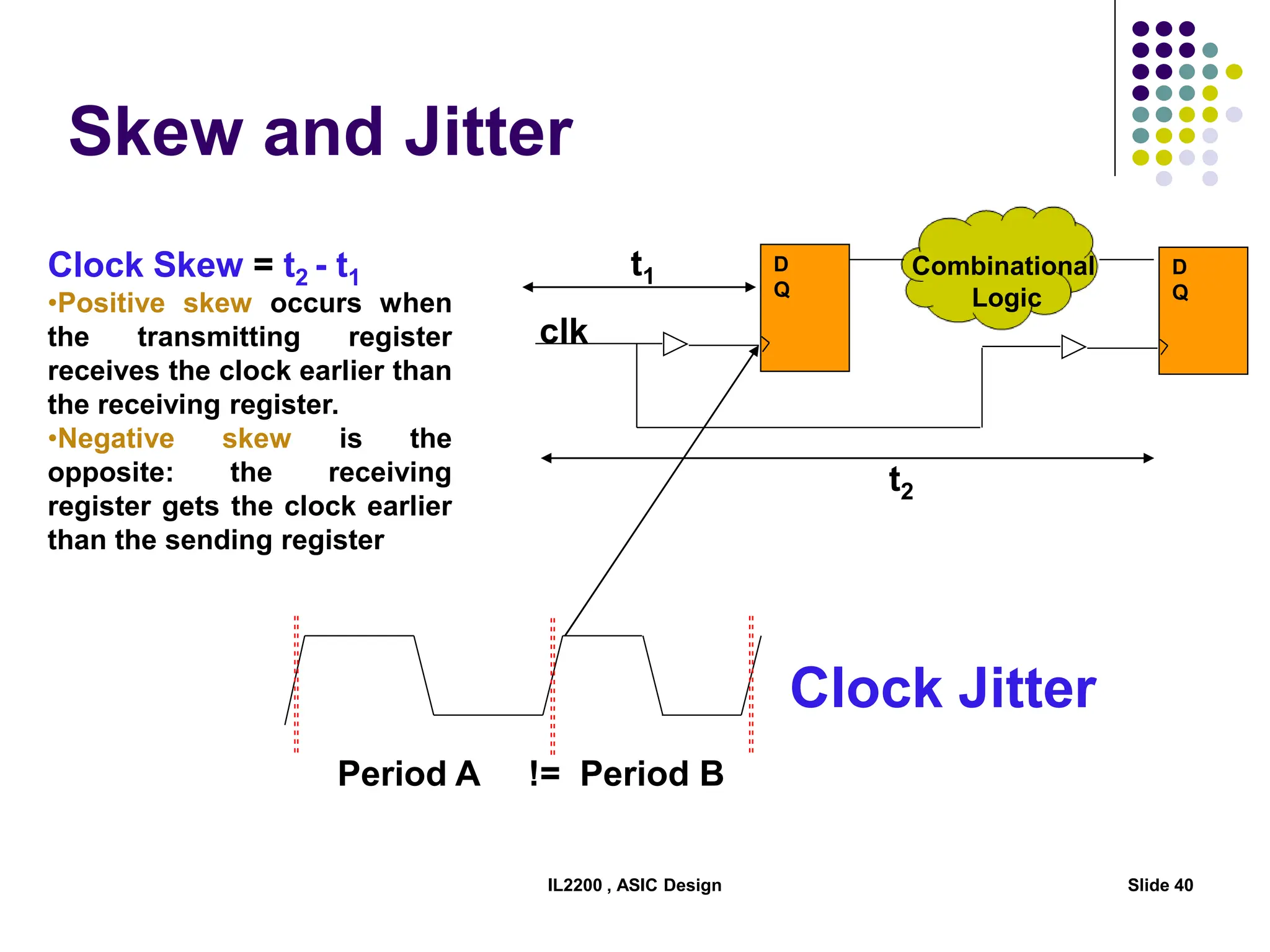
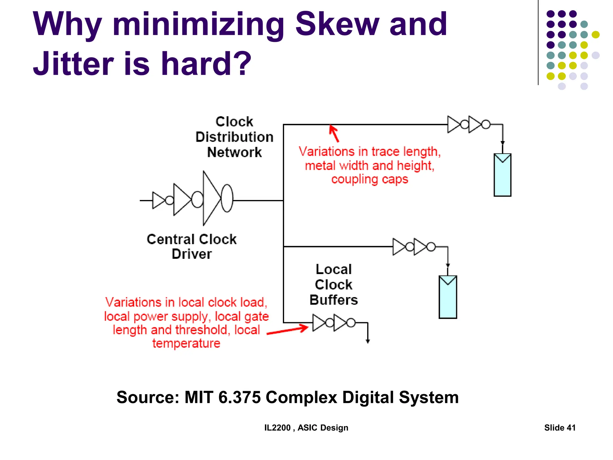

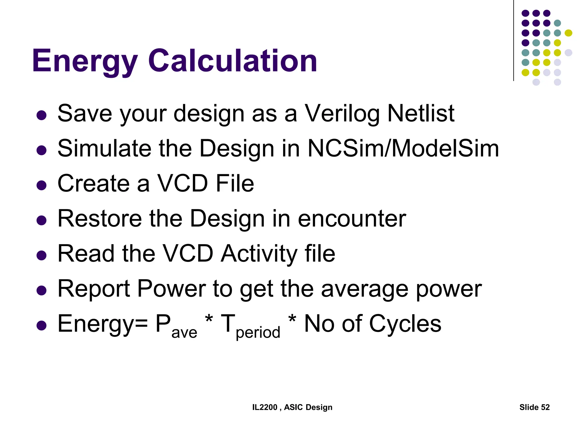

The document outlines the physical design aspects of ASIC design, covering topics such as implementation styles, design flow, floor planning, power planning, placement, and timing analysis. It details various methodologies for converting gate-level netlists into physical layouts, including the importance of optimization in routing and clock tree synthesis. Additionally, it discusses verification processes and energy calculations to ensure efficient functioning of the ASIC design.