10/03/2025
3
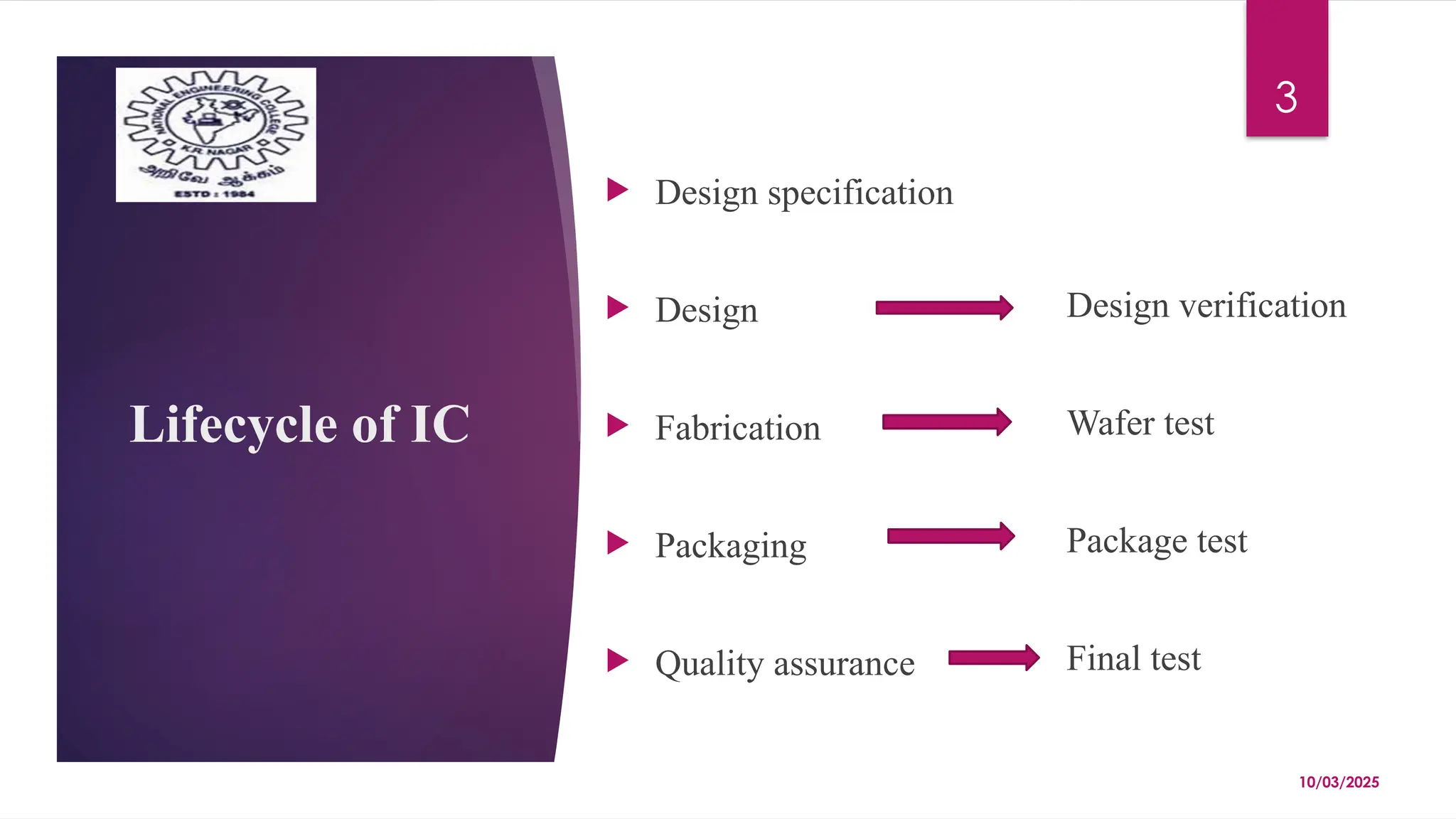
Lifecycle of IC
Design specification
Design
Fabrication
Packaging
Quality assurance
Design verification
Wafer test
Package test
Final test
10/03/2025
7
Architecture
Design
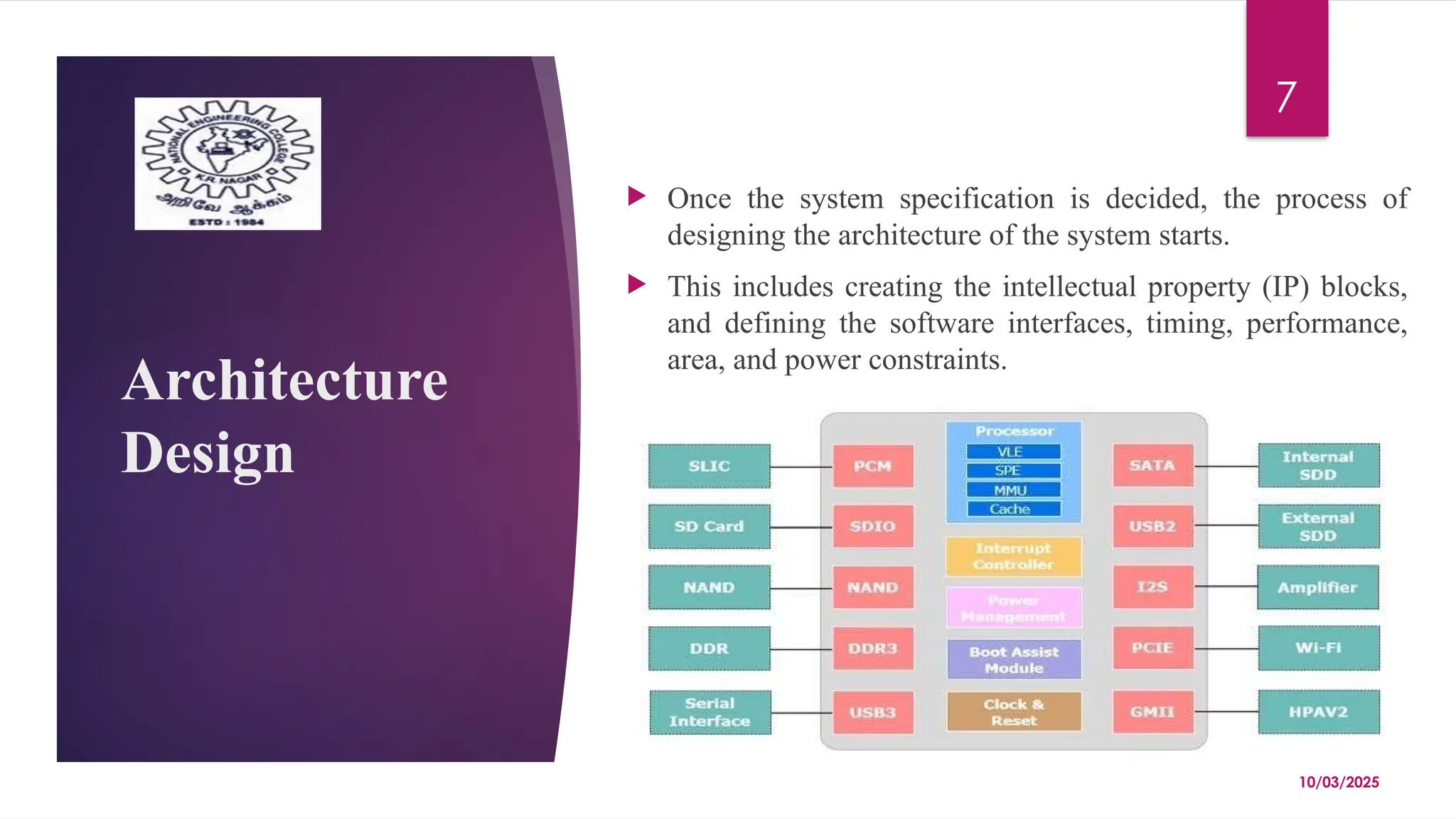
Once thesystem specification is decided, the process of
designing the architecture of the system starts.
This includes creating the intellectual property (IP) blocks,
and defining the software interfaces, timing, performance,
area, and power constraints.
8.
10/03/2025
8
Architecture
Verification
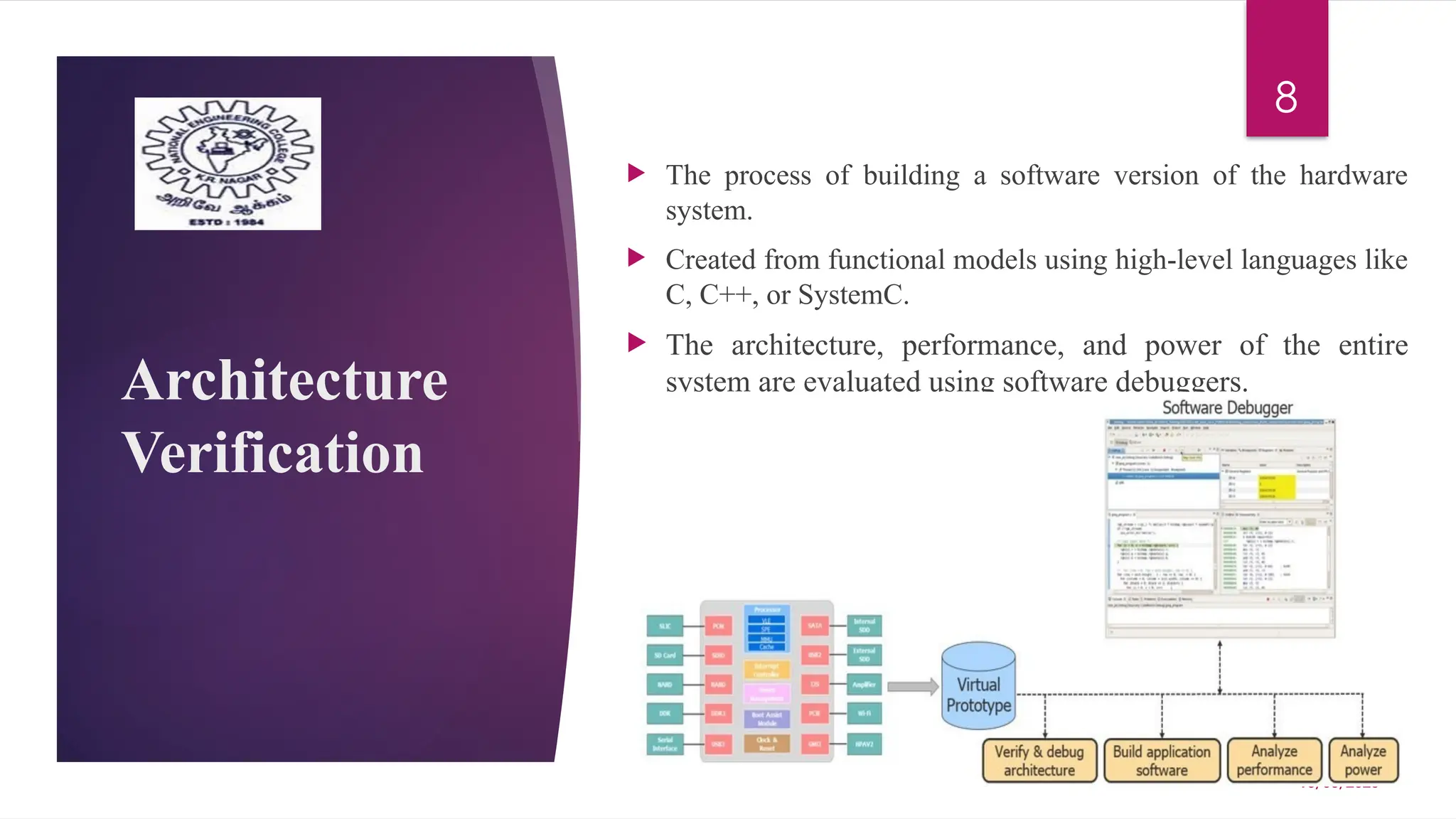
The processof building a software version of the hardware
system.
Created from functional models using high-level languages like
C, C++, or SystemC.
The architecture, performance, and power of the entire
system are evaluated using software debuggers.
9.
10/03/2025
9
Formal
Verification –
Property
Checking
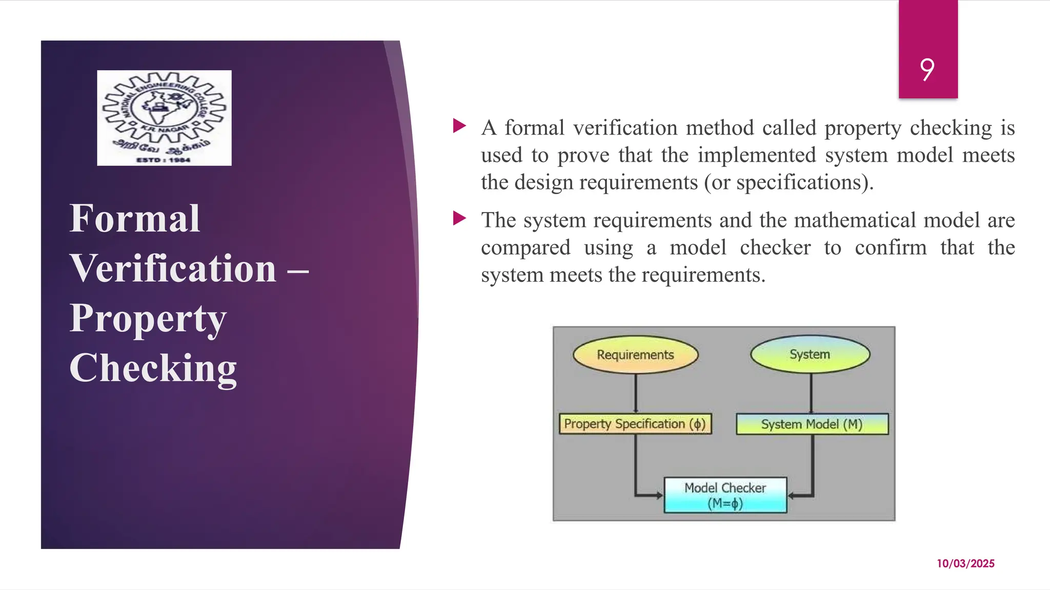
Aformal verification method called property checking is
used to prove that the implemented system model meets
the design requirements (or specifications).
The system requirements and the mathematical model are
compared using a model checker to confirm that the
system meets the requirements.
10.
10/03/2025
10
Design Entry
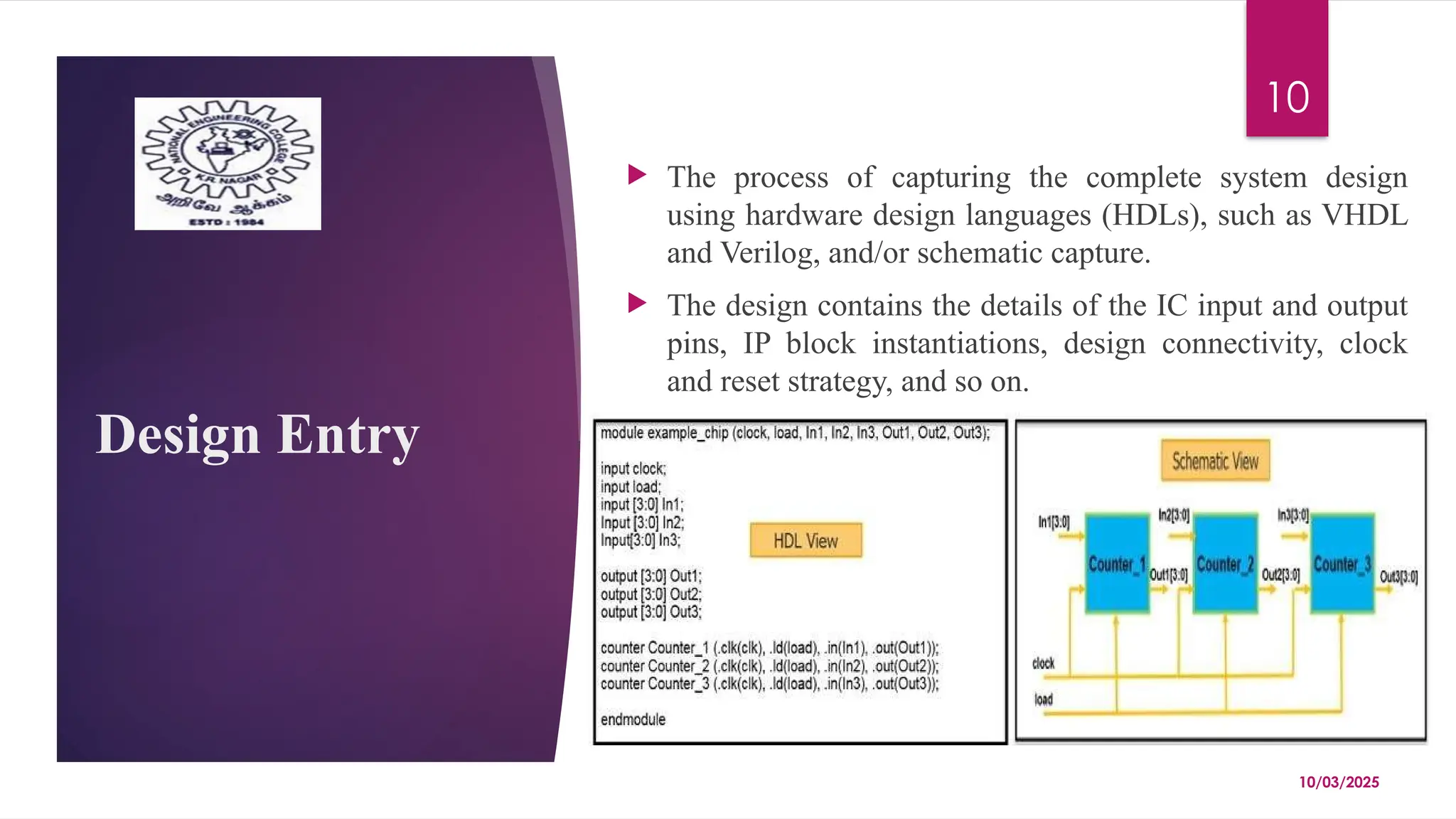
Theprocess of capturing the complete system design
using hardware design languages (HDLs), such as VHDL
and Verilog, and/or schematic capture.
The design contains the details of the IC input and output
pins, IP block instantiations, design connectivity, clock
and reset strategy, and so on.
11.
10/03/2025
11
Functional
Simulation
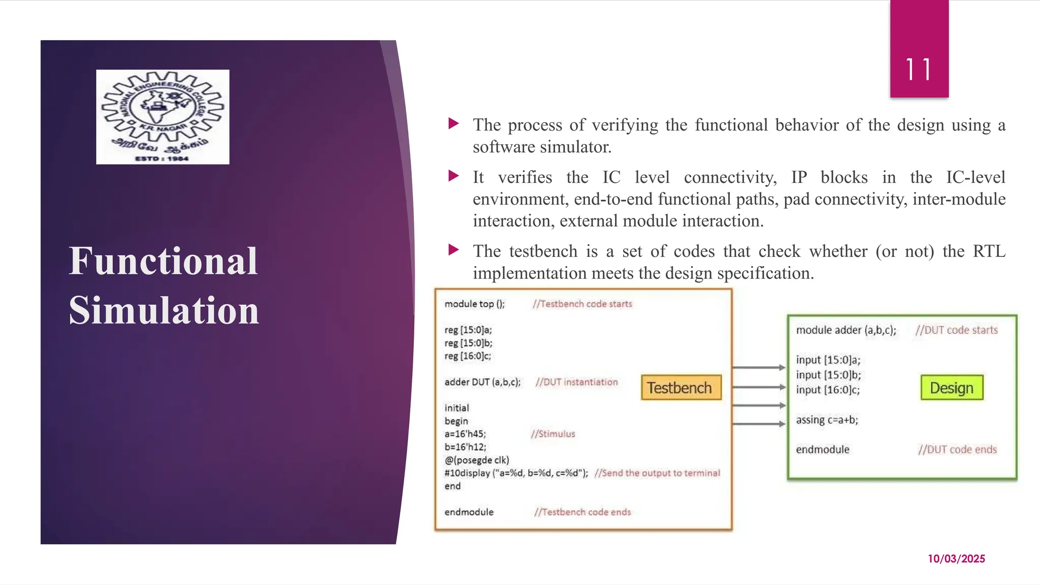
The processof verifying the functional behavior of the design using a
software simulator.
It verifies the IC level connectivity, IP blocks in the IC-level
environment, end-to-end functional paths, pad connectivity, inter-module
interaction, external module interaction.
The testbench is a set of codes that check whether (or not) the RTL
implementation meets the design specification.
12.
10/03/2025
12
Formal
Verification –
Equivalence
Checking
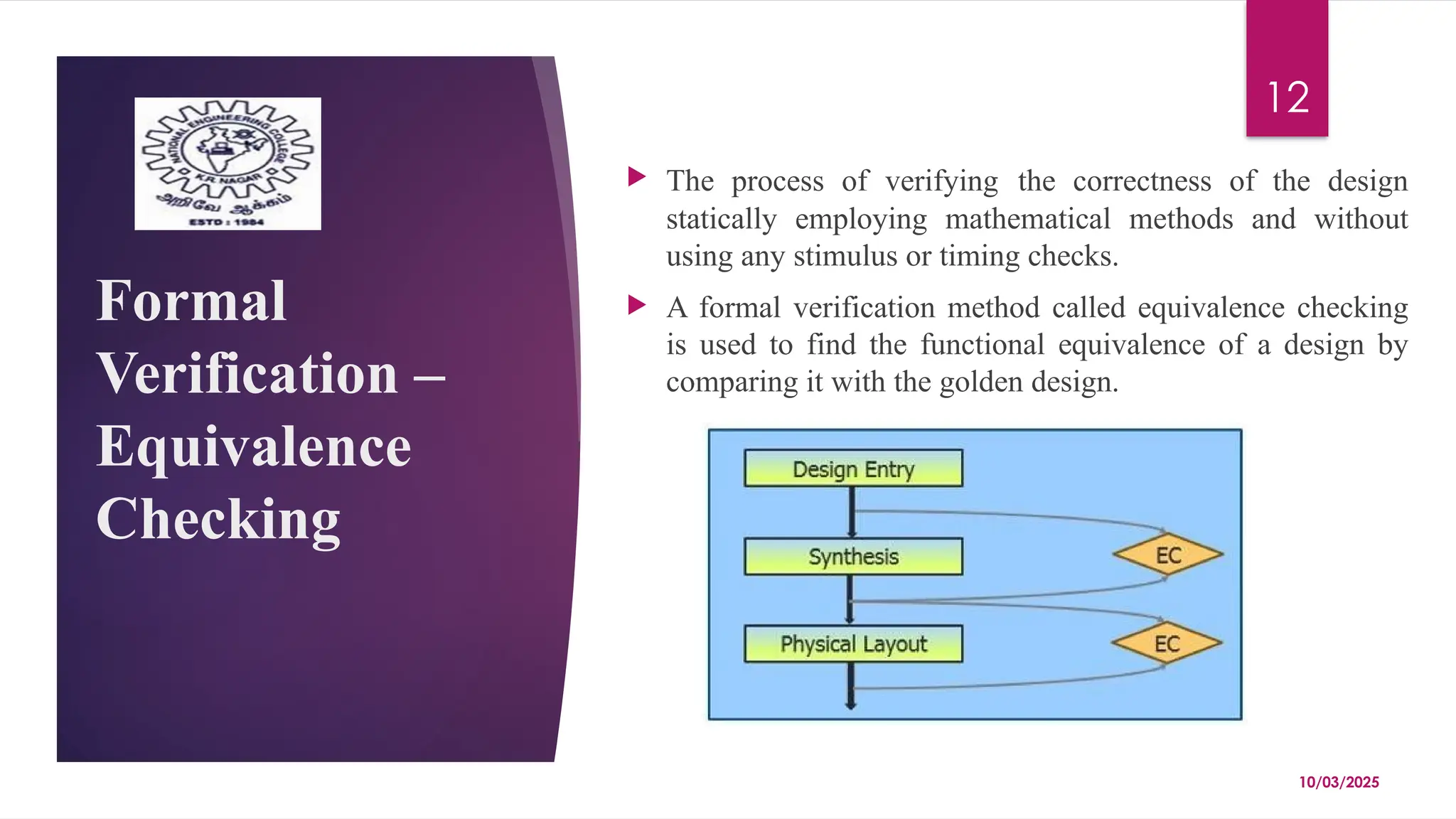
Theprocess of verifying the correctness of the design
statically employing mathematical methods and without
using any stimulus or timing checks.
A formal verification method called equivalence checking
is used to find the functional equivalence of a design by
comparing it with the golden design.
13.
10/03/2025
13
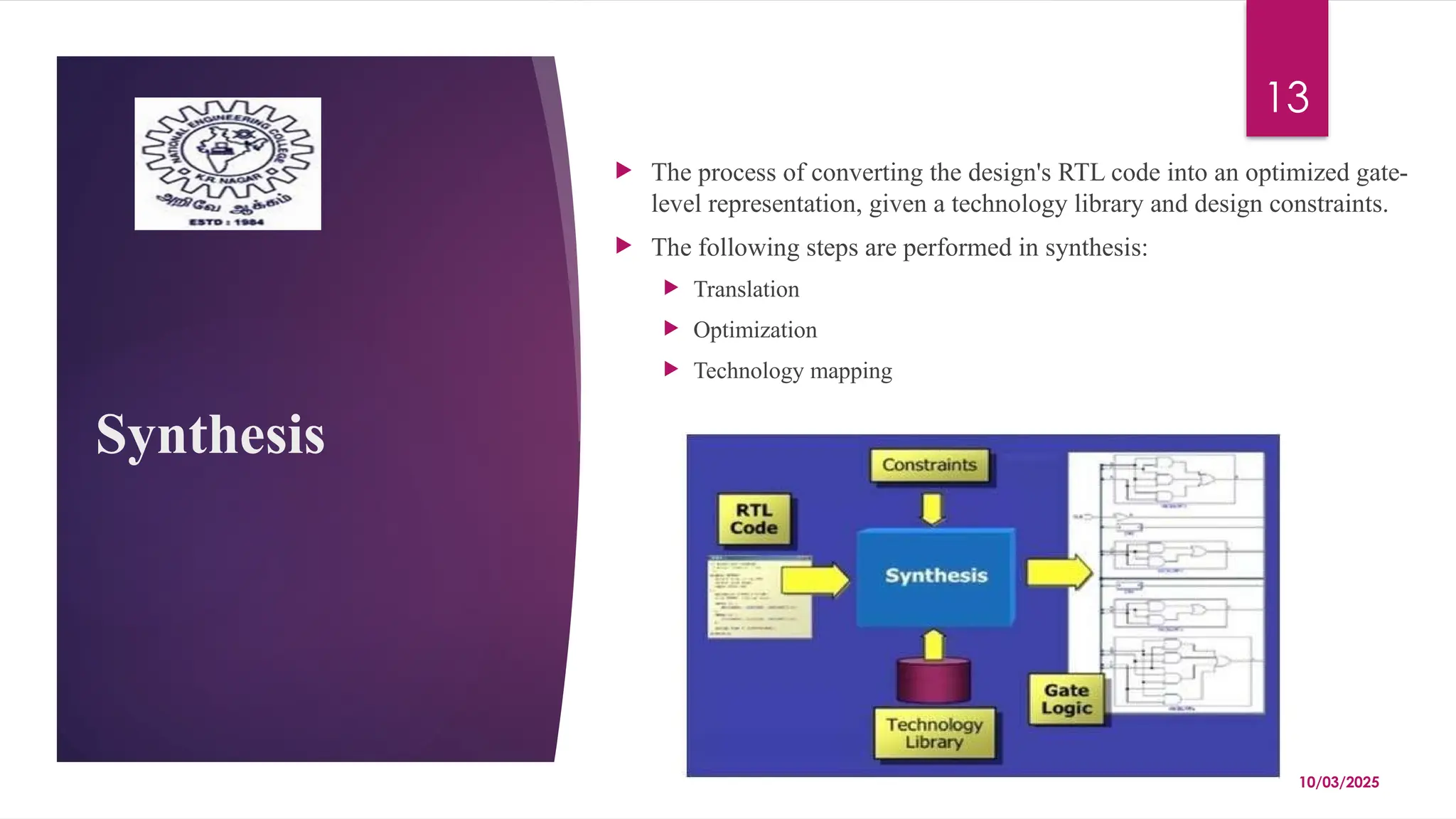
Synthesis
The processof converting the design's RTL code into an optimized gate-
level representation, given a technology library and design constraints.
The following steps are performed in synthesis:
Translation
Optimization
Technology mapping
14.
10/03/2025
14
Static Timing
Analysis (STA)
The process of verifying the timing characteristics of a
design without providing any stimulus.
STA is fast and exhaustive, but it doesn't check the
functionality of the design.
It is performed in various stages of the IC design cycle
15.
10/03/2025
15
Design for Test
(DFT)
The process of manufacturing an IC is not 100% error-
free.
Extra logic, known as Design for Test (DFT) logic, has
to be inserted in the design to aid in post-production
testing of the IC to identify manufacturing defects.
When an IC is manufactured, it is first checked for any
manufacturing defects with the help of the DFT logic.
If there are no manufacturing defects, then the IC is
checked for functional correctness.
10/03/2025
17
Physical Layout
Physicallayout is the transition from the logical view of
the IC to the physical view.
The output of the physical layout process is a Graphical
Database System (GDSII) file, which is a binary file
format representing planar geometrical shapes, text
labels, and other information related to the physical
layout.
The steps performed in physical layout are as follows:
Floor planning
Partitioning
Place and Route
Clock Tree Synthesis
18.
10/03/2025
18
Post – Layout
Simulation
Post-layout simulation is the process of verifying the
design after the physical layout of the design has been
established.
The checks performed in post-layout simulation are as
follows:
Design Rule Check (DRC)
Electrical Rule Check (ERC)
Layout Vs. Schematic (LVS)
19.
10/03/2025
19
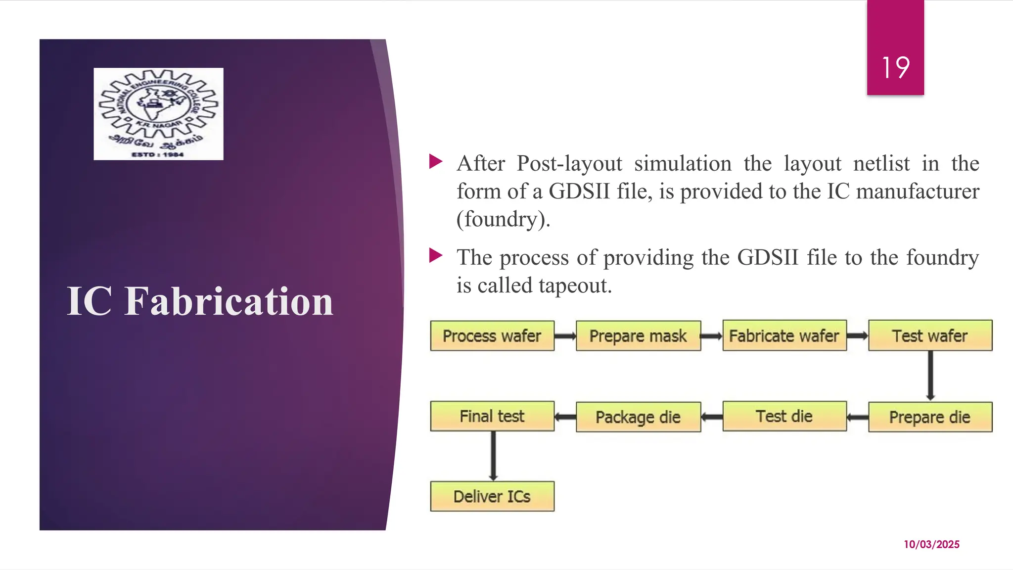
IC Fabrication
AfterPost-layout simulation the layout netlist in the
form of a GDSII file, is provided to the IC manufacturer
(foundry).
The process of providing the GDSII file to the foundry
is called tapeout.
20.
10/03/2025
20
IC Tester
ICmanufacturing isn't 100% reliable, resulting in many
samples that have manufacturing defects.
Once the IC is received from the foundry, a tester is
used to filter the defective ICs.
The tester provides input stimulus to the IC and verifies
the output.
It also verifies the electrical and thermal characteristics
of the IC and finds the ideal operating conditions.
21.
10/03/2025
21
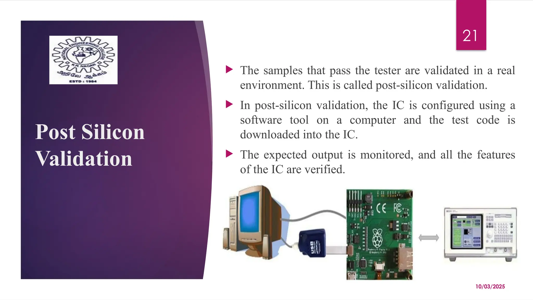
Post Silicon
Validation
Thesamples that pass the tester are validated in a real
environment. This is called post-silicon validation.
In post-silicon validation, the IC is configured using a
software tool on a computer and the test code is
downloaded into the IC.
The expected output is monitored, and all the features
of the IC are verified.
10/03/2025
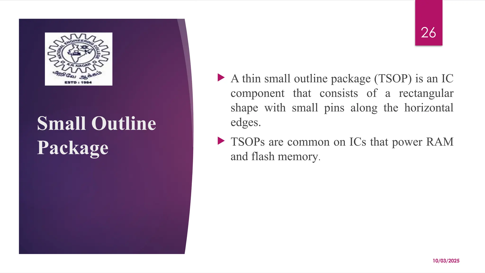
26
Small Outline
Package
Athin small outline package (TSOP) is an IC
component that consists of a rectangular
shape with small pins along the horizontal
edges.
TSOPs are common on ICs that power RAM
and flash memory.