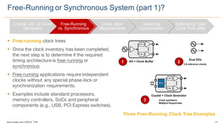
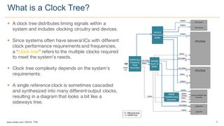
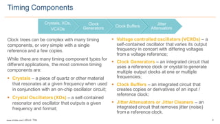
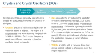
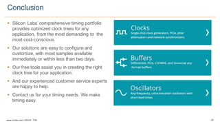
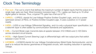
Clock Tree 101
3www.silabs.com  |  eBook  Title  
§ A  clock  tree  distributes  timing  signals  within  a  
system  and  includes  clocking  circuitry  and  devices.
§ Since systems often have several ICs with different
clock performance requirements and frequencies,
a “clock tree” refers to the multiple clocks required
to meet the system’s needs.
§ Clock  tree  complexity  depends  on  the  system’s  
requirements.
§ A single reference clock is sometimes cascaded
and synthesized into many different output clocks,
resulting in a diagram that looks a bit like a
sideways tree.
What  is  a  Clock  Tree?
4www.silabs.com  |  eBook  Title  
Clock  trees  can  be  complex  with  many  timing  
components,  or  very  simple  with  a  single  
reference  and  a  few  copies.  
While  there  are  many  timing  component  types  for  
different  applications,  the  most  common  timing  
components  are:
§ Crystals – a  piece  of  quartz  or  other  material  
that  resonates  at  a  given  frequency  when  used  
in  conjunction  with  an  on-­chip  oscillator  circuit;;  
§ Crystal  Oscillators  (XOs)  – a  self-­contained  
resonator  and  oscillator  that  outputs  a  given  
frequency  and  format;;
Timing  Components
Crystals,  XOs,
VCXOs
Clock  
Generators Clock  Buffers
Jitter  
Attenuators
§ Voltage  controlled  oscillators  (VCXOs)  – a  
self-­contained  oscillator  that  varies  its  output  
frequency  in  concert  with  differing  voltages  
from  a  voltage  reference;;
§ Clock  Generators  – an  integrated  circuit  that  
uses  a  reference  clock  or  crystal  to  generate  
multiple  output  clocks  at  one  or  multiple  
frequencies;;  
§ Clock  Buffers  – an  integrated  circuit  that  
creates  copies  or  derivatives  of  an  input  /    
reference  clock;;  
§ Jitter  Attenuators  or  Jitter  Cleaners  – an  
integrated  circuit  that  removes  jitter  (noise)  
from  a  reference  clock.
5www.silabs.com  |  eBook  Title  
Crystals  and  XOs  are  generally  cost-­effective  
unless  the  output  requirements  are  unusual  or  
stringent.  
§ Crystals  provide  a  frequency  output  when  an  
electrical  signal  is  applied.  The  output  is  a  
single-­ended sine  wave  typically  ranging  from  
32  kHz  to  50  MHz. Each  output  frequency  
requires  a  different  resonator  cut  and  an  
oscillator  circuit  to  operate.  
§ XOs integrate  the  crystal  with  the  oscillator  
circuit  in  a  standalone  package.  XOs  output  
either  a  LVCMOS  single-­ended or  differential  
square  wave.    Differential  signaling  is  used  in  
high-­speed,  jitter  sensitive  applications.  Some  
XOs  provide  multiple  frequencies  via  I2C  or  pin  
control.  XOs  are  generally  cost  effective  unless  
the  application  requires  a  variety  of  clock  
frequencies.
§ VXCOs  are  XOs  with  a  varactor  diode  that  
allows  applied  voltage  to  change  or  skew  the  
output  frequency.
Crystals  and  Crystal  Oscillators  (XOs)
Crystals,  XOs,  
and  VCXOs
Clock  
Generators Clock  Buffers
Jitter  
Attenuators
6www.silabs.com  |  eBook  Title  
Crystal  -­
single-­ended  sine  wave  
output
LVCMOS  XO  -­
single-­ended  square  wave  
output
Differential  XO/VCXO  -­
differential  or  complementary  
square  wave  output.  Note  
multiple  output  pins  for  
differential  signals.
Three  Common  Types  of  Frequency  Reference  Sources
Crystals,  XOs,  
and  VCXOs
Clock  
Generators Clock  Buffers
Jitter  
Attenuators
7www.silabs.com  |  eBook  Title  
Clock generators are integrated circuits (ICs)
that generate multiple output frequencies from a
single input reference frequency.
The input or reference frequency is supplied by a
crystal, XO or other clock in the system.
Clock generators may have other features that
are controlled by I2C or pins including
§ turning on/off outputs,
§ skewing frequencies, and
§ adding/removing spread spectrum to
frequencies to reduce noise.
The perceived challenge with clock generators is
system layout. Placing a crystal adjacent to its
target IC is simple and cheap. Routing a clock
signal from a clock generator to its target IC
might not be as easy, although it can save
money.
Careful design, and other techniques can ensure
a centralized clock source provides equal
performance. And, generally speaking, if four or
more clocks are required designers can save
money with a clock generator.
Clock  Generators
Crystals,  XOs,  
and  VCXOs
Clock  
Generators Clock  Buffers
Jitter  
Attenuators
8www.silabs.com  |  eBook  Title  
Low  Jitter  
PLL
Crystal
or
Ref  clock
Pin  or  I2
C
Silicon  Labs  Any-­
Frequency  Clock  
Generator
Output  
Clocks
Multi  
Synth  
Multi  
Synth  
Multi  
Synth  
Multi  
Synth  
Multi-­Format  
Drivers
§ The clock generator shown here is
programmable with up to eight single-ended
outputs or four differential outputs. It allows
designers to replace eight single-ended
crystals or four differential ones with a single
IC.
Clock  Generators
Crystals,  XOs,  
and  VCXOs
Clock  
Generators Clock  Buffers
Jitter  
Attenuators
Silicon  Labs’  Si5338  Clock  Generator  
“Any  Frequency  In  /  Any  Frequency  Out”
9www.silabs.com  |  eBook  Title  
Clock buffers distribute multiple copies or simple
derivatives of an input / reference clock.
The reference clock can be from a clock generator,
XO, or a system clock. Clock buffers scale their
input clock from 2 to more than 10 outputs.
They may include I2C, SPI, or pin-controlled
features like signal level and format translation,
voltage level translation, multiplexing, and input
frequency division.
These features save space and cost by eliminating
components, voltage dividers, and / or signal level
transition circuits.
Clock  Buffers
Silicon  Labs  Si5330x  Universal  Buffer
Pin
Control
Silicon  Labs  Universal  Clock  Buffer
Output  
Clocks
Input  
Clocks
Bank  A
Bank  B
DIV
DIV
Multi-­Format
Drivers
Crystals,  XOs,  
and  VCXOs
Glock  
Generators Clock  Buffers
Jitter  
Attenuators
10www.silabs.com  |  eBook  Title  
Jitter attenuators are clock generators with
specialized circuitry for reducing jitter (noise).
They may also be called clock cleaners or jitter
cleaners.
These highly specialized timing devices remove
jitter from incoming reference clocks and
minimize jitter in the system.
Jitter attenuators are typically used in high-speed
applications such as Synchronous Ethernet and
SDI Video to ensure that all physical layer data
transmission is synchronized.
Jitter  Attenuators
Crystals,  XOs,  
and  VCXOs
Glock  
Generators Glock  Buffers
Jitter  
Attenuators
DSPLL
IN
XTAL
Pin  or  I2
C/SPI
Silicon
Labs
Si5345 CLK0
CLK9
NVM
IN
Multi
Synth
Multi
Synth
/INT
/INT
FB_IN
OSC
Status  Control
Silicon Labs’  Si5345  
Jitter  Attenuating  Clock
11www.silabs.com  |  eBook  Title  
§ When starting a clock tree design, the design team needs to carefully assess the system
requirements and layout.
§ The system’s clocking requirements will determine what type of components to use, their
performance levels within the system and its overall network, and will also likely indicate whether
or not clock generators can provide signals or if crystals and XOs are needed. Of course, the
system may require a mixture of the various timing components.
§ The decisions to be addressed are…
§ Selecting a clock generator versus a crystal, XO or VCXO.
§ Determining if the system is free-running or synchronous.
§ Determining the system’s clock jitter requirements.
§ Selecting timing components that meet the system requirements.
§ Estimating the overall clock tree jitter with the selected components, and making adjustments if needed.
Critical  Clock  Tree  Design  Criteria
Crystal,  XO,  or  Clock  
Generator
Free-­Running  
vs.  Synchronous
Clock  Jitter  
Requirements
Selecting  
Components
Estimating  Total  
Clock  Tree  Jitter
12www.silabs.com  |  eBook  Title  
§ When to Use a Crystal vs a Clock
§ Crystals are typically used if the target IC has
an integrated oscillator and on-chip phase-
locked loops (PLLs) for internal timing.
§ Crystals are cost-effective components that
exhibit excellent phase noise and are widely
available.
§ They can also be placed in close proximity to
the IC, simplifying board layout.
§ One of the drawbacks of crystals is that their
frequency can vary significantly over
temperature, exceeding the parts-per-million
(ppm) stability requirements of some
applications.
§ In many stability-sensitive high-speed
applications, crystal oscillators (XOs) are a
better fit because they guarantee tighter
temperature stability.
Crystal,  XO,  or  Clock  Generator?
Crystal,  XO,  or  Clock  
Generator
Free-­Running  
vs.  Synchronous
Clock  Jitter  
Requirements
Selecting  
Components
Estimating  Total  
Clock  Tree  Jitter
13www.silabs.com  |  eBook  Title  
§ When to Use a Crystal vs a Clock
§ Clock generators and clock buffers are useful when several reference frequencies are required
and the target ICs are all on the same board or in the same IC or FPGA.
§ In some applications, FPGA/ASICs have multiple time domains for the data path, control plane
and memory controller interface, and as a result require multiple unique reference frequencies.
This is a good place for a clock generator.
§ A clock generator or buffer is also better when the IC cannot accommodate a crystal input, when
the IC must be synchronized to an external reference (source-synchronous application), or when a
high-frequency reference is required.
Crystal,  XO,  or  Clock  Generator?
Crystal,  XO,  or  Clock  
Generator
Free-­Running  
vs.  Synchronous
Clock  Jitter  
Requirements
Selecting  
Components
Estimating  Total  
Clock  Tree  Jitter
14www.silabs.com  |  eBook  Title  
§ Free-running clock trees
§ Once the clock inventory has been completed,
the next step is to determine if the required
timing architecture is free-running or
synchronous.
§ Free running applications require independent
clocks without any special phase-lock or
synchronization requirements.
§ Examples include standard processors,
memory controllers, SoCs and peripheral
components (e.g., USB, PCI Express switches).
Free-­Running  or  Synchronous  System  (part  1)?
Crystal,  XO,  or  Clock  
Generator
Free-­Running  
vs.  Synchronous
Clock  Jitter  
Requirements
Selecting  
Components
Estimating  Total  
Clock  Tree  Jitter
Three  Free-­Running  Clock  Tree  Examples
1 2
3
15www.silabs.com  |  eBook  Title  
§ Synchronous clock trees
§ Synchronous systems require continuous communication and network-level synchronization
across all associated systems.
§ In these applications, low-bandwidth PLL-based clocks provide jitter filtering to ensure that
network-level synchronization is maintained.
§ For example, synchronizing all SerDes (serialization-deserialization) reference clocks to a highly
accurate network reference clock (e.g., Stratum 3 or GPS) guarantees synchronization across all
system nodes.
Free-­Running  or  Synchronous  System  (part  2)?
Crystal,  XO,  or  Clock  
Generator
Free-­Running  
vs.  Synchronous
Clock  Jitter  
Requirements
Selecting  
Components
Estimating  Total  
Clock  Tree  Jitter
16www.silabs.com  |  eBook  Title  
§ Synchronous clock  trees  examples
§ Optical  Transport  Networking  (OTN)
§ SONET/SDH
Free-­Running  or  Synchronous  System  (part  2)?
Crystal,  XO,  or  Clock  
Generator
Free-­Running  
vs.  Synchronous
Clock  Jitter  
Requirements
Selecting  
Components
Estimating  Total  
Clock  Tree  Jitter
Synchronous  Clock  Tree  Example
§ Mobile  backhaul
§ Synchronous  Ethernet
§ HD  SDI  video  transmission
17www.silabs.com  |  eBook  Title  
§ Clock  jitter  is  a  critical  specification  for  timing  
components  since  clock  jitter  can  compromise  
system  performance.  
§ There  are  three  common  types  of  clock  
jitter,  and  depending  on  the  application,  one  
type  of  jitter  will  be  more  important  than  
another.
1. Cycle-­to-­cycle  jitter  measures  the  maximum  
change  in  the  clock  period  between  any  two  
adjacent  clock  cycles,  typically  measured  
over  1,000  cycles.  
2. Period  jitter  is  the  maximum  deviation  in  
clock  period  with  respect  to  an  ideal  period  
over  a  large  number  of  cycles  (10,000  is  
typical).
3. Phase  jitter  is  the  figure  of  merit  for  
demanding,  high-­speed  SerDes applications.  
It  is  a  ratio  of  noise  power  to  signal  power  
calculated  by  integrating  the  clock  single  
sideband  phase  noise  across  a  range  of  
frequencies  offset  from  a  carrier  signal.
Clock  Jitter  Requirements
Crystal,  XO,  or  Clock  
Generator
Free-­Running  
vs.  Synchronous
Clock  Jitter  
Requirements
Selecting  
Components
Estimating  Total  
Clock  Tree  Jitter
18www.silabs.com  |  eBook  Title  
§ Silicon  Labs  provides  a  detailed  investigation  of  timing  jitter  in  the  Timing  Jitter  Dictionary  and  
Technical  Guide.  
Clock  Jitter  Requirements
Crystal,  XO,  or  Clock  
Generator
Free-­Running  
vs.  Synchronous
Clock  Jitter  
Requirements
Selecting  
Components
Estimating  Total  
Clock  Tree  Jitter
Click  here  for
Silicon  Labs  Timing  
Jitter  Dictionary,  Tutorial,  and
Technical  Guide
19www.silabs.com  |  eBook  Title  
§ Jitter  performance  varies  across  a  wide  range  of  conditions  including  
§ Device  configuration
§ Operating  frequency,  
§ Signal  format,  
§ Input  clock  slew  rate  and  jitter,
§ Power  supply,  and  Power  supply  noise,  and  so  on.  
§ Select  devices  with  complete  jitter  specifications  (TYP  +  MAX).  “TYP”  alone  is  not  complete.
Clock  Jitter  Requirements
Crystal,  XO,  or  Clock  
Generator
Free-­Running  
vs.  Synchronous
Clock  Jitter  
Requirements
Selecting  
Components
Estimating  Total  
Clock  Tree  Jitter
MIN TYP MAX
20www.silabs.com  |  eBook  Title  
§ Evaluate  devices  based  on  maximum  (MAX) jitter  performance.  
§ Typical  (TYP)  data  sheet  specifications  do  not  guarantee  device  performance  over  all  
conditions.  
§ Device  performance  can  change  across  manufacturing  process,  supply  voltage,  temperature  and  
frequency  variation.  
§ Look  for  comprehensive  “Test  Conditions”  and  MAX  in  data  sheets,  as  shown  below.
Selecting  Components
Crystal,  XO,  or  Clock  
Generator
Free-­Running  
vs.  Synchronous
Clock  Jitter  
Requirements
Selecting  
Components
Estimating  Total  
Clock  Tree  Jitter
MIN TYP MAX
21www.silabs.com  |  eBook  Title  
§ The  total  clock  tree  jitter  should  be  estimated  to  determine  if  there  is  sufficient  system-­level  design  
margin  before  the  clock  tree  is  committed.  
§ A  component  with  poor  performance  can  compromise  the  whole  system’s  performance.
§ IMPORTANT:  
§ Total  jitter  is not the  sum  of  the  MAX  RMS  specifications of  each  component.  
§ Total  jitter  is the  root  of  the  sum  of  the  squares  of  each  device’s  MAX  RMS  jitter.  
Estimating  Total  Clock  Tree  Jitter,  End-­to-­End
Crystal,  XO,  or  Clock  
Generator
Free-­Running  
vs.  Synchronous
Clock  Jitter  
Requirements
Selecting  
Components
Estimating  Total  
Clock  Tree  Jitter
Formula  for  ’’The  Root  Sum  of  the  Squares’’  
22www.silabs.com  |  eBook  Title  
§ Silicon  Labs  offers  a  free,  on-­line  tool  to  convert  phase  noise  to  jitter  requirements  or  performance.
Estimating  Total  Clock  Tree  Jitter,  End-­to-­End
Click  here  for  Silicon  Labs’  free  “Phase  
Noise  to  Jitter  Calculator”  tool.
Crystal,  XO,  or  Clock  
Generator
Free-­Running  
vs.  Synchronous
Clock  Jitter  
Requirements
Selecting  
Components
Estimating  Total  
Clock  Tree  Jitter
23www.silabs.com  |  eBook  Title  
§ The  table  below  summarizes  many  other  selection  criteria  used  for  both  free-­running  and  
synchronous  clock  trees.  More  information  here:  http://www.silabs.com/timing.    
Estimating  Total  Clock  Tree  Jitter,  End-­to-­End
Function Crystal XO Clock Generator Clock Buffer Jitter Attenuator
Free-run operation No Yes Yes Yes Yes
Synchronous operation No No Yes Yes Yes
Clock multiplication No No Yes No Yes
Clock division No No Yes Yes Yes
Jitter cleaning No No No No Yes
Design complexity Low Low Medium Low Medium
Integration Low Low High High High
Key features that
simplify clock tree
design
Small form factor Any-frequency, any-output
Format/level
translation
Any-frequency clock
synthesis
Placement next to IC Format translation Integrated output mix Integrated loop filter
Glitchless switching btw clocks
at different frequencies
Output voltage
translation
Hitless switching
VDD level translation
Synchronous output
clock disable
Hold over on lock loss
Crystal,  XO,  or  Clock  
Generator
Free-­Running  
vs.  Synchronous
Clock  Jitter  
Requirements
Selecting  
Components
Estimating  Total  
Clock  Tree  Jitter
24www.silabs.com  |  eBook  Title  
§ Clock  trees  provide  a  fundamentally  important  part  of  the  system  and  must  be  optimized  for  
performance,  power,  and  cost.  
§ Silicon  Labs’  comprehensive  portfolio  applies  to  all  ranges  of  applications,  from  the  most  
demanding  to  the  most  cost  conscious.  
Optimizing  Clock  Trees  – Example  One
Clock  Tree  Challenges
§ FPGA/ASIC/PHY  require  diverse  
mix  of  frequencies,  formats  
§ High-­speed  10G+  clocks  must  have  
very  low  jitter
Silicon  Labs  Solution
§ Single  timing  component  generates  
all  required  frequencies
§ Best-­in-­class  jitter  (100  fs  RMS)
§ 4–10  clock  outputs
§ Saves  cost,  power,  and  space
Conventional  Approach Silicon  Labs  Solution
CPU/NPU
FPGA/ASIC/
SWITCH
1G  PHY
1G  PHY
10G  PHY
10G  PHY
161.1328125  MHz  (LVDS)
125  MHz  (LVPECL)
125  MHz  (LVPECL)
161.1328125  MHz  (LVDS)
100  MHz  (HCSL)
133.333  MHz  (CMOS)
83.333  MHZ  (CMOS)
50  MHz  (CMOS)
156.25  MHz  (LVDS)
156.25  MHz  (LVDS)
PCIe  3.0
CPU/NPU
FPGA/ASIC/
SWITCH
1G  PHY
1G  PHY
10G  PHY
10G  PHY
161.1328125  MHz  (LVDS)
125  MHz  (LVPECL)
156.25  MHz  (LVDS)
156.25  MHz  (LVDS)
50  MHz  (CMOS)
83.333  MHZ  (CMOS)
133.333  MHz  (CMOS)
100  MHz  (HCSL)
PCIe  3.0
Si5341
MultiSynth
MultiSynth
MultiSynth
MultiSynth
MultiSynth
Buffer
Clock
Clock
Buffer
25www.silabs.com  |  eBook  Title  
§ Clock  trees  provide  a  fundamentally  important  part  of  the  system  and  must  be  optimized  for  
performance,  power,  and  cost.  
§ Silicon  Labs’  comprehensive  portfolio  applies  to  all  ranges  of  applications,  from  the  most  
demanding  to  the  most  cost  conscious.  
Optimizing  Clock  Trees  – Example  Two
Clock  Tree  Challenges
§ Jitter  cleaning  required
§ FPGA/ASIC/PHY  requires  diverse  
mix  of  frequencies,  formats
§ High-­speed  10G+  clocks  must  have  
very  low  jitter
Silicon  Labs  Solution
§ Single  component  accepts  any  
frequency  and  cleans  jitter
§ Single  component  generates  any  
combination  of  frequencies
§ Best-­in-­class  jitter  (100  fs  RMS)
§ Saves  cost,  power,  and  space
Conventional  Approach Silicon  Labs  Solution
CPU/NPU
FPGA/ASIC/
SWITCH
1G  PHY
1G  PHY
10G  PHY
10G  PHY
125  MHz  (LVPECL)
125  MHz  (LVPECL)
100  MHz  (HCSL)
133.333  MHz  (CMOS)
83.333  MHZ  (CMOS)
50  MHz  (CMOS)
156.25  MHz  (LVDS)
156.25  MHz  (LVDS)
2.048  MHz
19.44  MHz
125  MHz
100  MHz
156.525  MHz  (LVDS)
155.52  MHz  (LVDS)
PCIe  3.0
DSPLL
Si5345
MultiSynth
MultiSynth
MultiSynth
MultiSynth
MultiSynth
CPU/NPU
FPGA/ASIC/
SWITCH
1G  PHY
1G  PHY
10G  PHY
10G  PHY
156.25  MHz  
(LVDS)
125  MHz  (LVPECL)
156.25  MHz  (LVDS)
156.25  MHz  (LVDS)
50  MHz  (CMOS)
83.333  MHz  (CMOS)
133.333  MHz  (CMOS)
100  MHz  (HCSL)
125  MHz  (LVPECL)2.048  MHz
19.44  MHz
125  MHz
100  MHz
155.52  MHz  
(LVDS)
PCIe  3.0
Clock
Clock
Gen
JA
Clock
26www.silabs.com  |  eBook  Title  
§ Silicon  Labs’  comprehensive  timing  portfolio  
provides  optimized  clock  trees  for  any  
application,  from  the  most  demanding  to    the  
most  cost-­conscious.  
§ Our  solutions  are  easy  to  configure  and  
customize,  with  most  samples  available  
immediately  or  within  less  than  two  days.  
§ Our  free  tools  assist  you  in  creating  the  right  
clock  tree  for  your  application.  
§ And  our  experienced  customer  service  experts  
are  happy  to  help.  
§ Contact  us  for  your  timing  needs.  We  make  
timing  easy.  
Conclusion
27www.silabs.com  |  eBook  Title  
§ Fan  out  – Fan  out  is  a  term  that  defines  the  maximum  number  of  digital  inputs  that  the  output  of  a  
single logic  gate can  feed.  Most  transistor-­transistor  logic  ( TTL )  gates  can  feed  up  to  10  other  
digital  gates  or  devices.  Thus,  a  typical  TTL  gate  has  a  fan-­out  of  10.
§ LVPECL  – LVPECL  stands  for  Low-­Voltage  Positive  Emitter-­Coupled  Logic,  and  it  is  a  power  
optimized  version  of  PECL  or  Positive  Emitter-­Coupled  Logic.  It  uses  a  positive  3.3  V  power  
supply.  
§ LVDS  – LVDS  is  Low-­Voltage  Differential  Signaling,  and  it  is  only  a  physical  layer  specification,  but  
a  data  link  layer  is  often  added  by  communication  standards  and  applications.  
§ CML  – Current  Mode  Logic  transmits  data  at  speeds  between  312.5  Mbit/s  and  3.125  Gbit/s  
across  standard  circuit  boards.  
§ HCSL  – High-­Speed  Current  Steering  Logic  is  differential  logic  with  two  output  pins  that  switch  
between  0  and  14  mA.  
§ LVCMOS  – LVCMOS  stands  for  Low  Voltage  Complementary  Metal  Oxide  Semiconductor,  and  its  
goal  is  to  reduce  the  device  geometries  of  integrated  circuits,  with  resulting  reduction  in  operating  
voltage.  
Clock  Tree  Terminology  
28www.silabs.com  |  eBook  Title  
§ Linda  Lua  is  the  Silicon  Labs  product  manager  for  datacenter  timing  products,  managing  the  
datacenter  clock  generators  and  clock  buffers  portfolio,  new  product  launches,  new  product  
initiatives  and  marketing  promotions.  
§ Prior  to  joining  Silicon  Labs,  Ms.  Lua  was  at  ISSI,  responsible  for  High  Speed  Memory  products,  
and  at  IDT  Inc.,  responsible  for  timing  products  business  development  and  product  management  in  
networking  and  the  communications  market.  
§ Ms.  Lua  holds  a  BS  in  Electrical  Engineering  from  Iowa  State  University  and  MBA  from  the  
University  of  Texas  at  Dallas.
About  the  Author
Clock Tree Timing 101

Clock Tree Timing 101

  • 2.
  • 3.
    3www.silabs.com  |  eBook Title   § A  clock  tree  distributes  timing  signals  within  a   system  and  includes  clocking  circuitry  and  devices. § Since systems often have several ICs with different clock performance requirements and frequencies, a “clock tree” refers to the multiple clocks required to meet the system’s needs. § Clock  tree  complexity  depends  on  the  system’s   requirements. § A single reference clock is sometimes cascaded and synthesized into many different output clocks, resulting in a diagram that looks a bit like a sideways tree. What  is  a  Clock  Tree?
  • 4.
    4www.silabs.com  |  eBook Title   Clock  trees  can  be  complex  with  many  timing   components,  or  very  simple  with  a  single   reference  and  a  few  copies.   While  there  are  many  timing  component  types  for   different  applications,  the  most  common  timing   components  are: § Crystals – a  piece  of  quartz  or  other  material   that  resonates  at  a  given  frequency  when  used   in  conjunction  with  an  on-­chip  oscillator  circuit;;   § Crystal  Oscillators  (XOs)  – a  self-­contained   resonator  and  oscillator  that  outputs  a  given   frequency  and  format;; Timing  Components Crystals,  XOs, VCXOs Clock   Generators Clock  Buffers Jitter   Attenuators § Voltage  controlled  oscillators  (VCXOs)  – a   self-­contained  oscillator  that  varies  its  output   frequency  in  concert  with  differing  voltages   from  a  voltage  reference;; § Clock  Generators  – an  integrated  circuit  that   uses  a  reference  clock  or  crystal  to  generate   multiple  output  clocks  at  one  or  multiple   frequencies;;   § Clock  Buffers  – an  integrated  circuit  that   creates  copies  or  derivatives  of  an  input  /     reference  clock;;   § Jitter  Attenuators  or  Jitter  Cleaners  – an   integrated  circuit  that  removes  jitter  (noise)   from  a  reference  clock.
  • 5.
    5www.silabs.com  |  eBook Title   Crystals  and  XOs  are  generally  cost-­effective   unless  the  output  requirements  are  unusual  or   stringent.   § Crystals  provide  a  frequency  output  when  an   electrical  signal  is  applied.  The  output  is  a   single-­ended sine  wave  typically  ranging  from   32  kHz  to  50  MHz. Each  output  frequency   requires  a  different  resonator  cut  and  an   oscillator  circuit  to  operate.   § XOs integrate  the  crystal  with  the  oscillator   circuit  in  a  standalone  package.  XOs  output   either  a  LVCMOS  single-­ended or  differential   square  wave.    Differential  signaling  is  used  in   high-­speed,  jitter  sensitive  applications.  Some   XOs  provide  multiple  frequencies  via  I2C  or  pin   control.  XOs  are  generally  cost  effective  unless   the  application  requires  a  variety  of  clock   frequencies. § VXCOs  are  XOs  with  a  varactor  diode  that   allows  applied  voltage  to  change  or  skew  the   output  frequency. Crystals  and  Crystal  Oscillators  (XOs) Crystals,  XOs,   and  VCXOs Clock   Generators Clock  Buffers Jitter   Attenuators
  • 6.
    6www.silabs.com  |  eBook Title   Crystal  -­ single-­ended  sine  wave   output LVCMOS  XO  -­ single-­ended  square  wave   output Differential  XO/VCXO  -­ differential  or  complementary   square  wave  output.  Note   multiple  output  pins  for   differential  signals. Three  Common  Types  of  Frequency  Reference  Sources Crystals,  XOs,   and  VCXOs Clock   Generators Clock  Buffers Jitter   Attenuators
  • 7.
    7www.silabs.com  |  eBook Title   Clock generators are integrated circuits (ICs) that generate multiple output frequencies from a single input reference frequency. The input or reference frequency is supplied by a crystal, XO or other clock in the system. Clock generators may have other features that are controlled by I2C or pins including § turning on/off outputs, § skewing frequencies, and § adding/removing spread spectrum to frequencies to reduce noise. The perceived challenge with clock generators is system layout. Placing a crystal adjacent to its target IC is simple and cheap. Routing a clock signal from a clock generator to its target IC might not be as easy, although it can save money. Careful design, and other techniques can ensure a centralized clock source provides equal performance. And, generally speaking, if four or more clocks are required designers can save money with a clock generator. Clock  Generators Crystals,  XOs,   and  VCXOs Clock   Generators Clock  Buffers Jitter   Attenuators
  • 8.
    8www.silabs.com  |  eBook Title   Low  Jitter   PLL Crystal or Ref  clock Pin  or  I2 C Silicon  Labs  Any-­ Frequency  Clock   Generator Output   Clocks Multi   Synth   Multi   Synth   Multi   Synth   Multi   Synth   Multi-­Format   Drivers § The clock generator shown here is programmable with up to eight single-ended outputs or four differential outputs. It allows designers to replace eight single-ended crystals or four differential ones with a single IC. Clock  Generators Crystals,  XOs,   and  VCXOs Clock   Generators Clock  Buffers Jitter   Attenuators Silicon  Labs’  Si5338  Clock  Generator   “Any  Frequency  In  /  Any  Frequency  Out”
  • 9.
    9www.silabs.com  |  eBook Title   Clock buffers distribute multiple copies or simple derivatives of an input / reference clock. The reference clock can be from a clock generator, XO, or a system clock. Clock buffers scale their input clock from 2 to more than 10 outputs. They may include I2C, SPI, or pin-controlled features like signal level and format translation, voltage level translation, multiplexing, and input frequency division. These features save space and cost by eliminating components, voltage dividers, and / or signal level transition circuits. Clock  Buffers Silicon  Labs  Si5330x  Universal  Buffer Pin Control Silicon  Labs  Universal  Clock  Buffer Output   Clocks Input   Clocks Bank  A Bank  B DIV DIV Multi-­Format Drivers Crystals,  XOs,   and  VCXOs Glock   Generators Clock  Buffers Jitter   Attenuators
  • 10.
    10www.silabs.com  |  eBook Title   Jitter attenuators are clock generators with specialized circuitry for reducing jitter (noise). They may also be called clock cleaners or jitter cleaners. These highly specialized timing devices remove jitter from incoming reference clocks and minimize jitter in the system. Jitter attenuators are typically used in high-speed applications such as Synchronous Ethernet and SDI Video to ensure that all physical layer data transmission is synchronized. Jitter  Attenuators Crystals,  XOs,   and  VCXOs Glock   Generators Glock  Buffers Jitter   Attenuators DSPLL IN XTAL Pin  or  I2 C/SPI Silicon Labs Si5345 CLK0 CLK9 NVM IN Multi Synth Multi Synth /INT /INT FB_IN OSC Status  Control Silicon Labs’  Si5345   Jitter  Attenuating  Clock
  • 11.
    11www.silabs.com  |  eBook Title   § When starting a clock tree design, the design team needs to carefully assess the system requirements and layout. § The system’s clocking requirements will determine what type of components to use, their performance levels within the system and its overall network, and will also likely indicate whether or not clock generators can provide signals or if crystals and XOs are needed. Of course, the system may require a mixture of the various timing components. § The decisions to be addressed are… § Selecting a clock generator versus a crystal, XO or VCXO. § Determining if the system is free-running or synchronous. § Determining the system’s clock jitter requirements. § Selecting timing components that meet the system requirements. § Estimating the overall clock tree jitter with the selected components, and making adjustments if needed. Critical  Clock  Tree  Design  Criteria Crystal,  XO,  or  Clock   Generator Free-­Running   vs.  Synchronous Clock  Jitter   Requirements Selecting   Components Estimating  Total   Clock  Tree  Jitter
  • 12.
    12www.silabs.com  |  eBook Title   § When to Use a Crystal vs a Clock § Crystals are typically used if the target IC has an integrated oscillator and on-chip phase- locked loops (PLLs) for internal timing. § Crystals are cost-effective components that exhibit excellent phase noise and are widely available. § They can also be placed in close proximity to the IC, simplifying board layout. § One of the drawbacks of crystals is that their frequency can vary significantly over temperature, exceeding the parts-per-million (ppm) stability requirements of some applications. § In many stability-sensitive high-speed applications, crystal oscillators (XOs) are a better fit because they guarantee tighter temperature stability. Crystal,  XO,  or  Clock  Generator? Crystal,  XO,  or  Clock   Generator Free-­Running   vs.  Synchronous Clock  Jitter   Requirements Selecting   Components Estimating  Total   Clock  Tree  Jitter
  • 13.
    13www.silabs.com  |  eBook Title   § When to Use a Crystal vs a Clock § Clock generators and clock buffers are useful when several reference frequencies are required and the target ICs are all on the same board or in the same IC or FPGA. § In some applications, FPGA/ASICs have multiple time domains for the data path, control plane and memory controller interface, and as a result require multiple unique reference frequencies. This is a good place for a clock generator. § A clock generator or buffer is also better when the IC cannot accommodate a crystal input, when the IC must be synchronized to an external reference (source-synchronous application), or when a high-frequency reference is required. Crystal,  XO,  or  Clock  Generator? Crystal,  XO,  or  Clock   Generator Free-­Running   vs.  Synchronous Clock  Jitter   Requirements Selecting   Components Estimating  Total   Clock  Tree  Jitter
  • 14.
    14www.silabs.com  |  eBook Title   § Free-running clock trees § Once the clock inventory has been completed, the next step is to determine if the required timing architecture is free-running or synchronous. § Free running applications require independent clocks without any special phase-lock or synchronization requirements. § Examples include standard processors, memory controllers, SoCs and peripheral components (e.g., USB, PCI Express switches). Free-­Running  or  Synchronous  System  (part  1)? Crystal,  XO,  or  Clock   Generator Free-­Running   vs.  Synchronous Clock  Jitter   Requirements Selecting   Components Estimating  Total   Clock  Tree  Jitter Three  Free-­Running  Clock  Tree  Examples 1 2 3
  • 15.
    15www.silabs.com  |  eBook Title   § Synchronous clock trees § Synchronous systems require continuous communication and network-level synchronization across all associated systems. § In these applications, low-bandwidth PLL-based clocks provide jitter filtering to ensure that network-level synchronization is maintained. § For example, synchronizing all SerDes (serialization-deserialization) reference clocks to a highly accurate network reference clock (e.g., Stratum 3 or GPS) guarantees synchronization across all system nodes. Free-­Running  or  Synchronous  System  (part  2)? Crystal,  XO,  or  Clock   Generator Free-­Running   vs.  Synchronous Clock  Jitter   Requirements Selecting   Components Estimating  Total   Clock  Tree  Jitter
  • 16.
    16www.silabs.com  |  eBook Title   § Synchronous clock  trees  examples § Optical  Transport  Networking  (OTN) § SONET/SDH Free-­Running  or  Synchronous  System  (part  2)? Crystal,  XO,  or  Clock   Generator Free-­Running   vs.  Synchronous Clock  Jitter   Requirements Selecting   Components Estimating  Total   Clock  Tree  Jitter Synchronous  Clock  Tree  Example § Mobile  backhaul § Synchronous  Ethernet § HD  SDI  video  transmission
  • 17.
    17www.silabs.com  |  eBook Title   § Clock  jitter  is  a  critical  specification  for  timing   components  since  clock  jitter  can  compromise   system  performance.   § There  are  three  common  types  of  clock   jitter,  and  depending  on  the  application,  one   type  of  jitter  will  be  more  important  than   another. 1. Cycle-­to-­cycle  jitter  measures  the  maximum   change  in  the  clock  period  between  any  two   adjacent  clock  cycles,  typically  measured   over  1,000  cycles.   2. Period  jitter  is  the  maximum  deviation  in   clock  period  with  respect  to  an  ideal  period   over  a  large  number  of  cycles  (10,000  is   typical). 3. Phase  jitter  is  the  figure  of  merit  for   demanding,  high-­speed  SerDes applications.   It  is  a  ratio  of  noise  power  to  signal  power   calculated  by  integrating  the  clock  single   sideband  phase  noise  across  a  range  of   frequencies  offset  from  a  carrier  signal. Clock  Jitter  Requirements Crystal,  XO,  or  Clock   Generator Free-­Running   vs.  Synchronous Clock  Jitter   Requirements Selecting   Components Estimating  Total   Clock  Tree  Jitter
  • 18.
    18www.silabs.com  |  eBook Title   § Silicon  Labs  provides  a  detailed  investigation  of  timing  jitter  in  the  Timing  Jitter  Dictionary  and   Technical  Guide.   Clock  Jitter  Requirements Crystal,  XO,  or  Clock   Generator Free-­Running   vs.  Synchronous Clock  Jitter   Requirements Selecting   Components Estimating  Total   Clock  Tree  Jitter Click  here  for Silicon  Labs  Timing   Jitter  Dictionary,  Tutorial,  and Technical  Guide
  • 19.
    19www.silabs.com  |  eBook Title   § Jitter  performance  varies  across  a  wide  range  of  conditions  including   § Device  configuration § Operating  frequency,   § Signal  format,   § Input  clock  slew  rate  and  jitter, § Power  supply,  and  Power  supply  noise,  and  so  on.   § Select  devices  with  complete  jitter  specifications  (TYP  +  MAX).  “TYP”  alone  is  not  complete. Clock  Jitter  Requirements Crystal,  XO,  or  Clock   Generator Free-­Running   vs.  Synchronous Clock  Jitter   Requirements Selecting   Components Estimating  Total   Clock  Tree  Jitter MIN TYP MAX
  • 20.
    20www.silabs.com  |  eBook Title   § Evaluate  devices  based  on  maximum  (MAX) jitter  performance.   § Typical  (TYP)  data  sheet  specifications  do  not  guarantee  device  performance  over  all   conditions.   § Device  performance  can  change  across  manufacturing  process,  supply  voltage,  temperature  and   frequency  variation.   § Look  for  comprehensive  “Test  Conditions”  and  MAX  in  data  sheets,  as  shown  below. Selecting  Components Crystal,  XO,  or  Clock   Generator Free-­Running   vs.  Synchronous Clock  Jitter   Requirements Selecting   Components Estimating  Total   Clock  Tree  Jitter MIN TYP MAX
  • 21.
    21www.silabs.com  |  eBook Title   § The  total  clock  tree  jitter  should  be  estimated  to  determine  if  there  is  sufficient  system-­level  design   margin  before  the  clock  tree  is  committed.   § A  component  with  poor  performance  can  compromise  the  whole  system’s  performance. § IMPORTANT:   § Total  jitter  is not the  sum  of  the  MAX  RMS  specifications of  each  component.   § Total  jitter  is the  root  of  the  sum  of  the  squares  of  each  device’s  MAX  RMS  jitter.   Estimating  Total  Clock  Tree  Jitter,  End-­to-­End Crystal,  XO,  or  Clock   Generator Free-­Running   vs.  Synchronous Clock  Jitter   Requirements Selecting   Components Estimating  Total   Clock  Tree  Jitter Formula  for  ’’The  Root  Sum  of  the  Squares’’  
  • 22.
    22www.silabs.com  |  eBook Title   § Silicon  Labs  offers  a  free,  on-­line  tool  to  convert  phase  noise  to  jitter  requirements  or  performance. Estimating  Total  Clock  Tree  Jitter,  End-­to-­End Click  here  for  Silicon  Labs’  free  “Phase   Noise  to  Jitter  Calculator”  tool. Crystal,  XO,  or  Clock   Generator Free-­Running   vs.  Synchronous Clock  Jitter   Requirements Selecting   Components Estimating  Total   Clock  Tree  Jitter
  • 23.
    23www.silabs.com  |  eBook Title   § The  table  below  summarizes  many  other  selection  criteria  used  for  both  free-­running  and   synchronous  clock  trees.  More  information  here:  http://www.silabs.com/timing.     Estimating  Total  Clock  Tree  Jitter,  End-­to-­End Function Crystal XO Clock Generator Clock Buffer Jitter Attenuator Free-run operation No Yes Yes Yes Yes Synchronous operation No No Yes Yes Yes Clock multiplication No No Yes No Yes Clock division No No Yes Yes Yes Jitter cleaning No No No No Yes Design complexity Low Low Medium Low Medium Integration Low Low High High High Key features that simplify clock tree design Small form factor Any-frequency, any-output Format/level translation Any-frequency clock synthesis Placement next to IC Format translation Integrated output mix Integrated loop filter Glitchless switching btw clocks at different frequencies Output voltage translation Hitless switching VDD level translation Synchronous output clock disable Hold over on lock loss Crystal,  XO,  or  Clock   Generator Free-­Running   vs.  Synchronous Clock  Jitter   Requirements Selecting   Components Estimating  Total   Clock  Tree  Jitter
  • 24.
    24www.silabs.com  |  eBook Title   § Clock  trees  provide  a  fundamentally  important  part  of  the  system  and  must  be  optimized  for   performance,  power,  and  cost.   § Silicon  Labs’  comprehensive  portfolio  applies  to  all  ranges  of  applications,  from  the  most   demanding  to  the  most  cost  conscious.   Optimizing  Clock  Trees  – Example  One Clock  Tree  Challenges § FPGA/ASIC/PHY  require  diverse   mix  of  frequencies,  formats   § High-­speed  10G+  clocks  must  have   very  low  jitter Silicon  Labs  Solution § Single  timing  component  generates   all  required  frequencies § Best-­in-­class  jitter  (100  fs  RMS) § 4–10  clock  outputs § Saves  cost,  power,  and  space Conventional  Approach Silicon  Labs  Solution CPU/NPU FPGA/ASIC/ SWITCH 1G  PHY 1G  PHY 10G  PHY 10G  PHY 161.1328125  MHz  (LVDS) 125  MHz  (LVPECL) 125  MHz  (LVPECL) 161.1328125  MHz  (LVDS) 100  MHz  (HCSL) 133.333  MHz  (CMOS) 83.333  MHZ  (CMOS) 50  MHz  (CMOS) 156.25  MHz  (LVDS) 156.25  MHz  (LVDS) PCIe  3.0 CPU/NPU FPGA/ASIC/ SWITCH 1G  PHY 1G  PHY 10G  PHY 10G  PHY 161.1328125  MHz  (LVDS) 125  MHz  (LVPECL) 156.25  MHz  (LVDS) 156.25  MHz  (LVDS) 50  MHz  (CMOS) 83.333  MHZ  (CMOS) 133.333  MHz  (CMOS) 100  MHz  (HCSL) PCIe  3.0 Si5341 MultiSynth MultiSynth MultiSynth MultiSynth MultiSynth Buffer Clock Clock Buffer
  • 25.
    25www.silabs.com  |  eBook Title   § Clock  trees  provide  a  fundamentally  important  part  of  the  system  and  must  be  optimized  for   performance,  power,  and  cost.   § Silicon  Labs’  comprehensive  portfolio  applies  to  all  ranges  of  applications,  from  the  most   demanding  to  the  most  cost  conscious.   Optimizing  Clock  Trees  – Example  Two Clock  Tree  Challenges § Jitter  cleaning  required § FPGA/ASIC/PHY  requires  diverse   mix  of  frequencies,  formats § High-­speed  10G+  clocks  must  have   very  low  jitter Silicon  Labs  Solution § Single  component  accepts  any   frequency  and  cleans  jitter § Single  component  generates  any   combination  of  frequencies § Best-­in-­class  jitter  (100  fs  RMS) § Saves  cost,  power,  and  space Conventional  Approach Silicon  Labs  Solution CPU/NPU FPGA/ASIC/ SWITCH 1G  PHY 1G  PHY 10G  PHY 10G  PHY 125  MHz  (LVPECL) 125  MHz  (LVPECL) 100  MHz  (HCSL) 133.333  MHz  (CMOS) 83.333  MHZ  (CMOS) 50  MHz  (CMOS) 156.25  MHz  (LVDS) 156.25  MHz  (LVDS) 2.048  MHz 19.44  MHz 125  MHz 100  MHz 156.525  MHz  (LVDS) 155.52  MHz  (LVDS) PCIe  3.0 DSPLL Si5345 MultiSynth MultiSynth MultiSynth MultiSynth MultiSynth CPU/NPU FPGA/ASIC/ SWITCH 1G  PHY 1G  PHY 10G  PHY 10G  PHY 156.25  MHz   (LVDS) 125  MHz  (LVPECL) 156.25  MHz  (LVDS) 156.25  MHz  (LVDS) 50  MHz  (CMOS) 83.333  MHz  (CMOS) 133.333  MHz  (CMOS) 100  MHz  (HCSL) 125  MHz  (LVPECL)2.048  MHz 19.44  MHz 125  MHz 100  MHz 155.52  MHz   (LVDS) PCIe  3.0 Clock Clock Gen JA Clock
  • 26.
    26www.silabs.com  |  eBook Title   § Silicon  Labs’  comprehensive  timing  portfolio   provides  optimized  clock  trees  for  any   application,  from  the  most  demanding  to    the   most  cost-­conscious.   § Our  solutions  are  easy  to  configure  and   customize,  with  most  samples  available   immediately  or  within  less  than  two  days.   § Our  free  tools  assist  you  in  creating  the  right   clock  tree  for  your  application.   § And  our  experienced  customer  service  experts   are  happy  to  help.   § Contact  us  for  your  timing  needs.  We  make   timing  easy.   Conclusion
  • 27.
    27www.silabs.com  |  eBook Title   § Fan  out  – Fan  out  is  a  term  that  defines  the  maximum  number  of  digital  inputs  that  the  output  of  a   single logic  gate can  feed.  Most  transistor-­transistor  logic  ( TTL )  gates  can  feed  up  to  10  other   digital  gates  or  devices.  Thus,  a  typical  TTL  gate  has  a  fan-­out  of  10. § LVPECL  – LVPECL  stands  for  Low-­Voltage  Positive  Emitter-­Coupled  Logic,  and  it  is  a  power   optimized  version  of  PECL  or  Positive  Emitter-­Coupled  Logic.  It  uses  a  positive  3.3  V  power   supply.   § LVDS  – LVDS  is  Low-­Voltage  Differential  Signaling,  and  it  is  only  a  physical  layer  specification,  but   a  data  link  layer  is  often  added  by  communication  standards  and  applications.   § CML  – Current  Mode  Logic  transmits  data  at  speeds  between  312.5  Mbit/s  and  3.125  Gbit/s   across  standard  circuit  boards.   § HCSL  – High-­Speed  Current  Steering  Logic  is  differential  logic  with  two  output  pins  that  switch   between  0  and  14  mA.   § LVCMOS  – LVCMOS  stands  for  Low  Voltage  Complementary  Metal  Oxide  Semiconductor,  and  its   goal  is  to  reduce  the  device  geometries  of  integrated  circuits,  with  resulting  reduction  in  operating   voltage.   Clock  Tree  Terminology  
  • 28.
    28www.silabs.com  |  eBook Title   § Linda  Lua  is  the  Silicon  Labs  product  manager  for  datacenter  timing  products,  managing  the   datacenter  clock  generators  and  clock  buffers  portfolio,  new  product  launches,  new  product   initiatives  and  marketing  promotions.   § Prior  to  joining  Silicon  Labs,  Ms.  Lua  was  at  ISSI,  responsible  for  High  Speed  Memory  products,   and  at  IDT  Inc.,  responsible  for  timing  products  business  development  and  product  management  in   networking  and  the  communications  market.   § Ms.  Lua  holds  a  BS  in  Electrical  Engineering  from  Iowa  State  University  and  MBA  from  the   University  of  Texas  at  Dallas. About  the  Author