Downloaded 38 times


![ASIC Engineering Organization
Engineering Talent
Project Oriented
Rigorous Processes
Best-in-Class Tools
Secure Infrastructure
System Redundancy
Specification Driven
Compliance Exit Criteria
Design for Test, Yield,
Manufacturability
True IP reuse culture
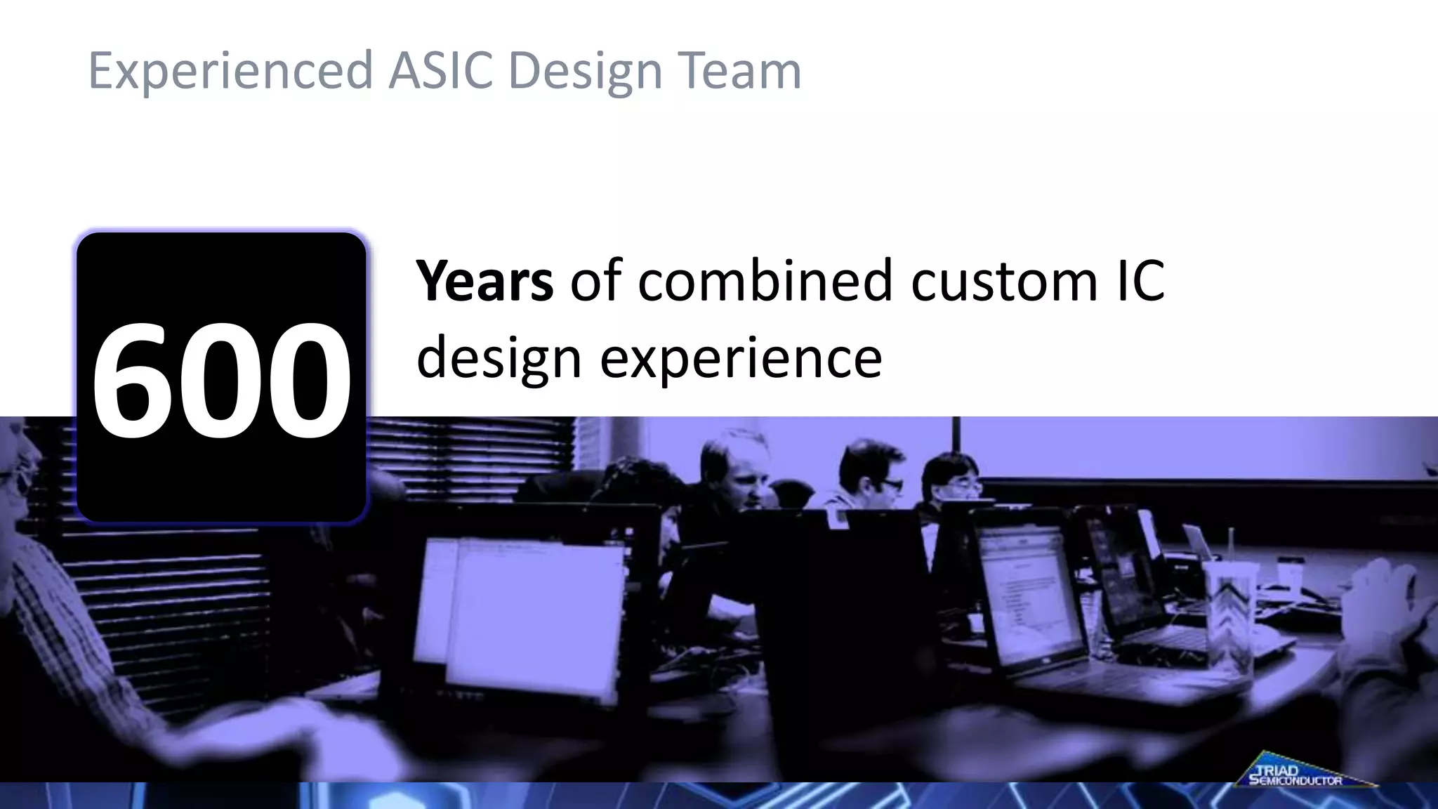
Triad’s Custom IC Engineering Group
25 IC Designers
Customers
Project Leaders [10]
IC Designers [15]
Project
Admins [2]
Test
Engineers [3]
Cad Engineer
Sys Admin
VP of Engineering](https://image.slidesharecdn.com/triadsemiconductormay2015-150527185703-lva1-app6892/75/Triad-Semiconductor-Analog-and-Mixed-Signal-ASIC-Company-Overview-7-2048.jpg)
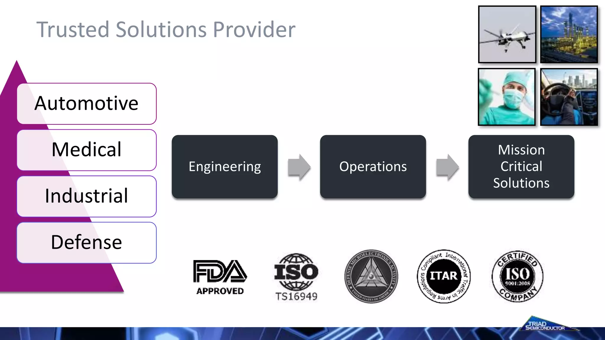
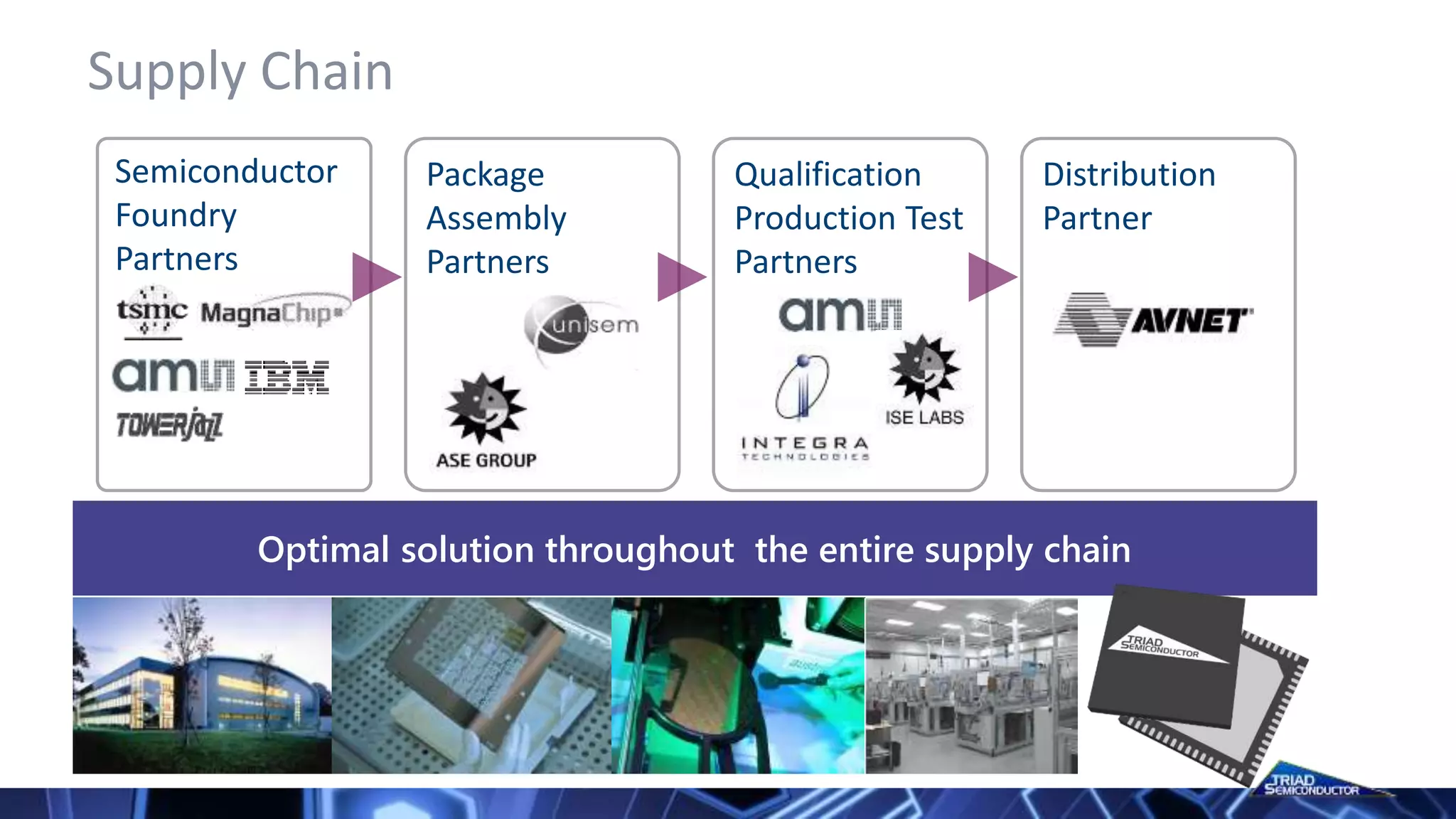

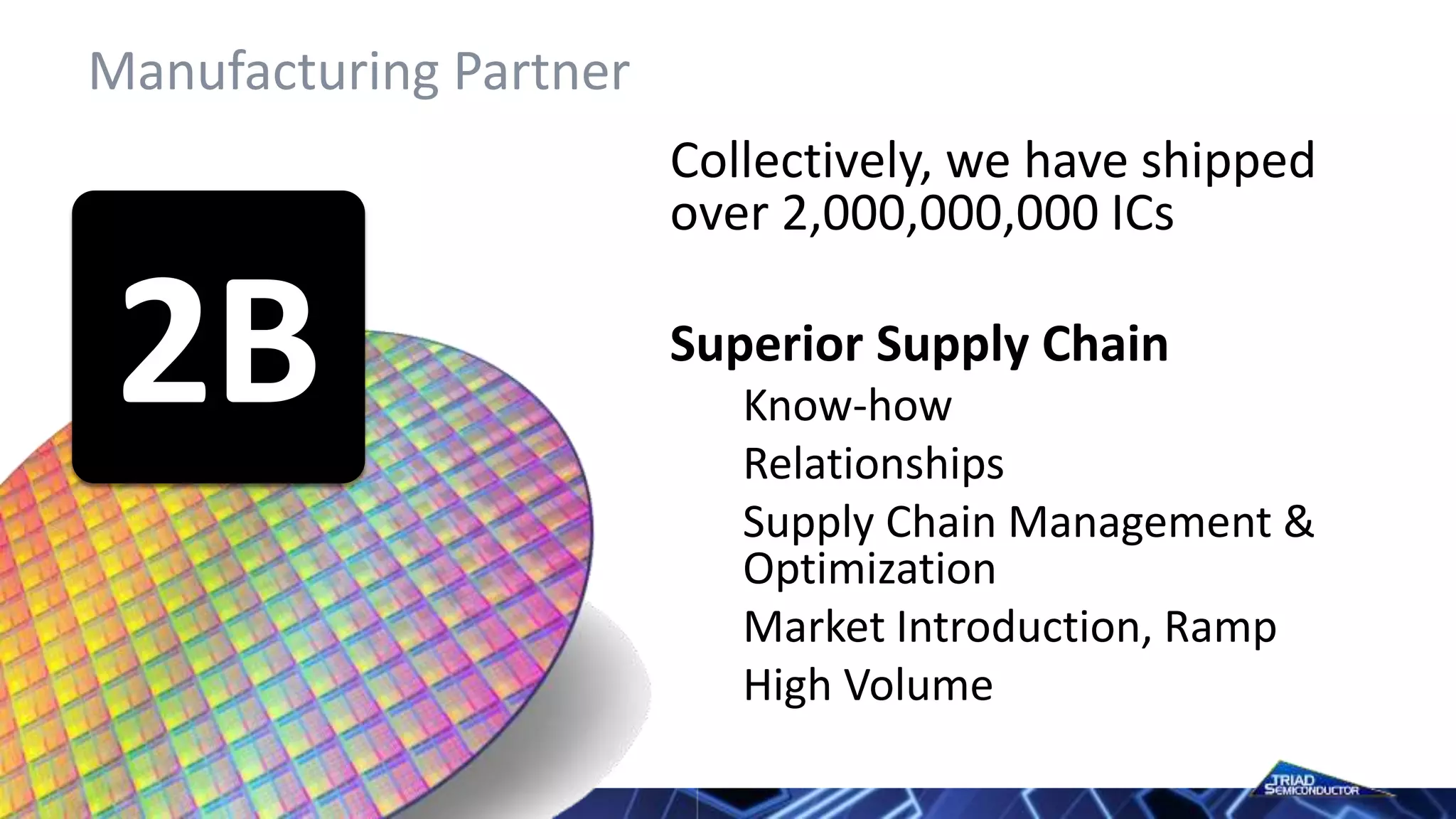
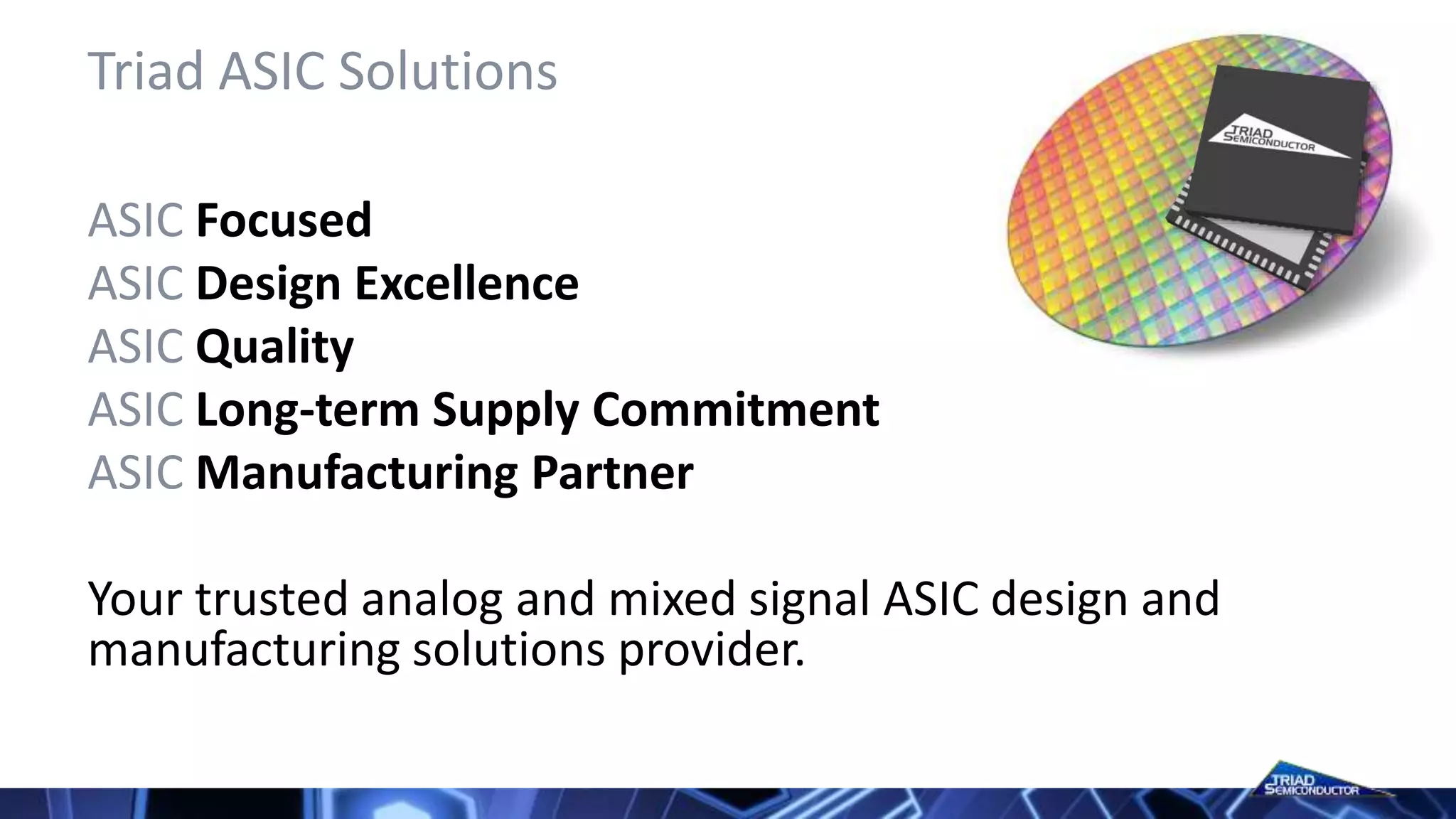
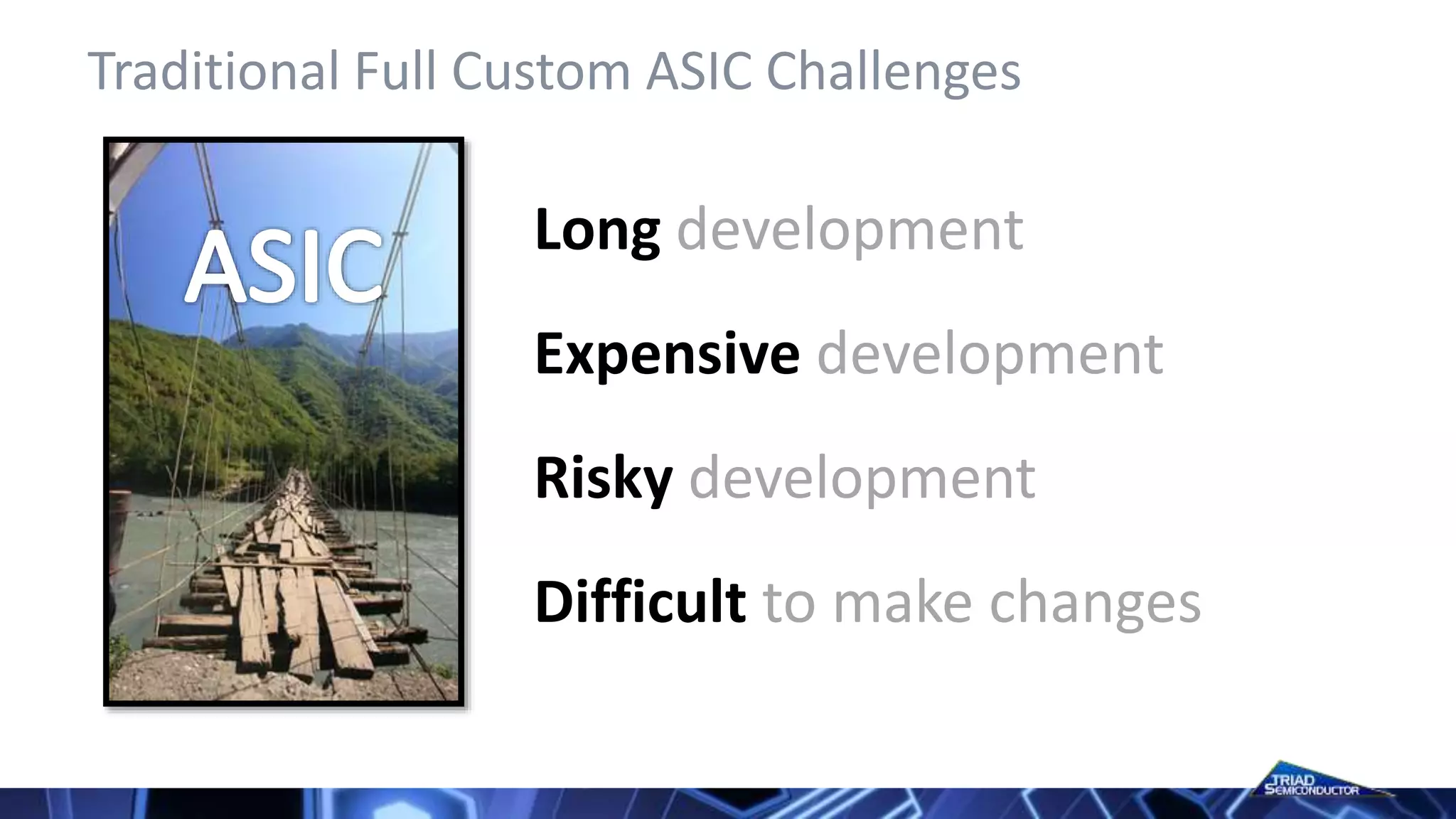

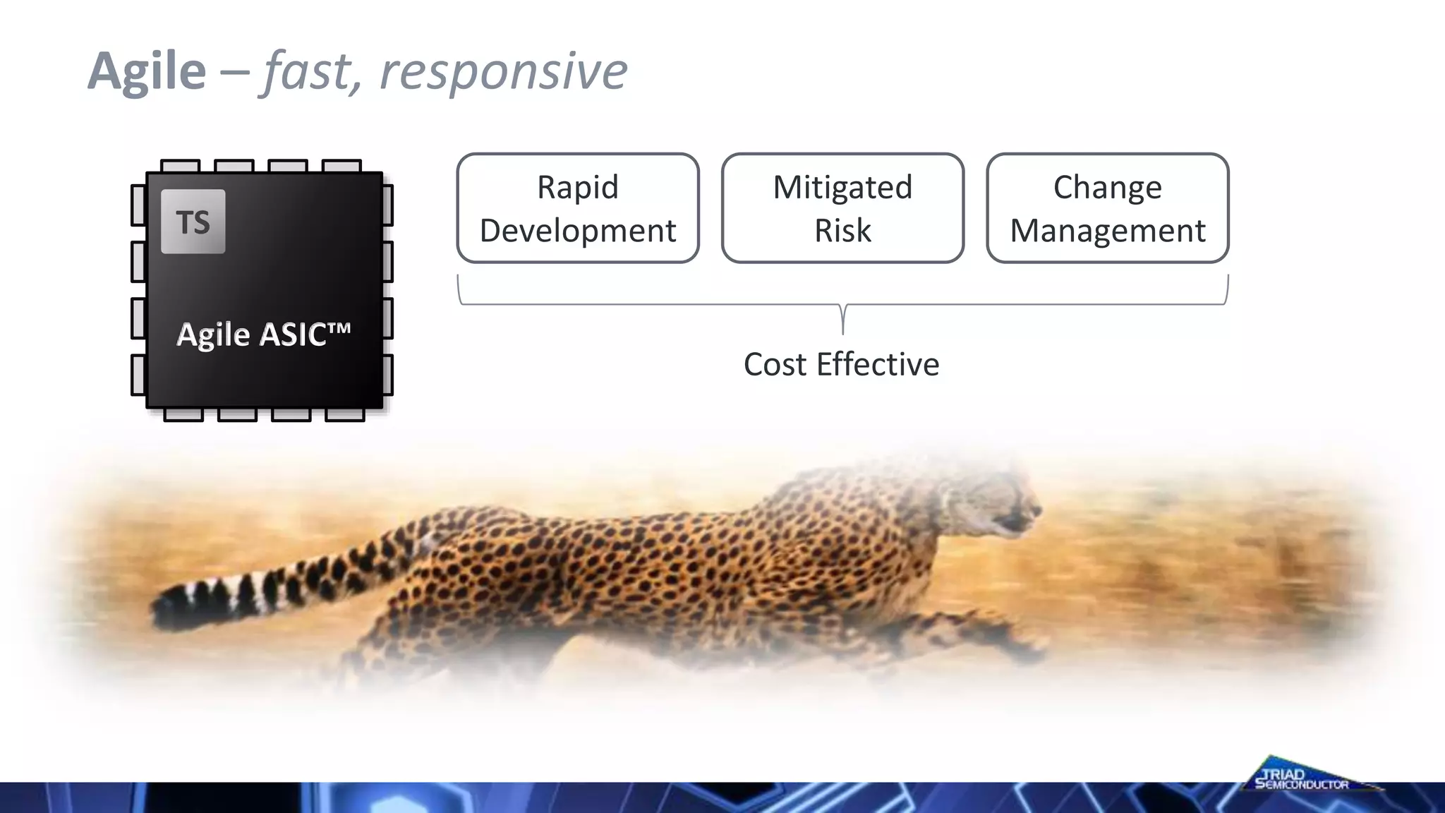
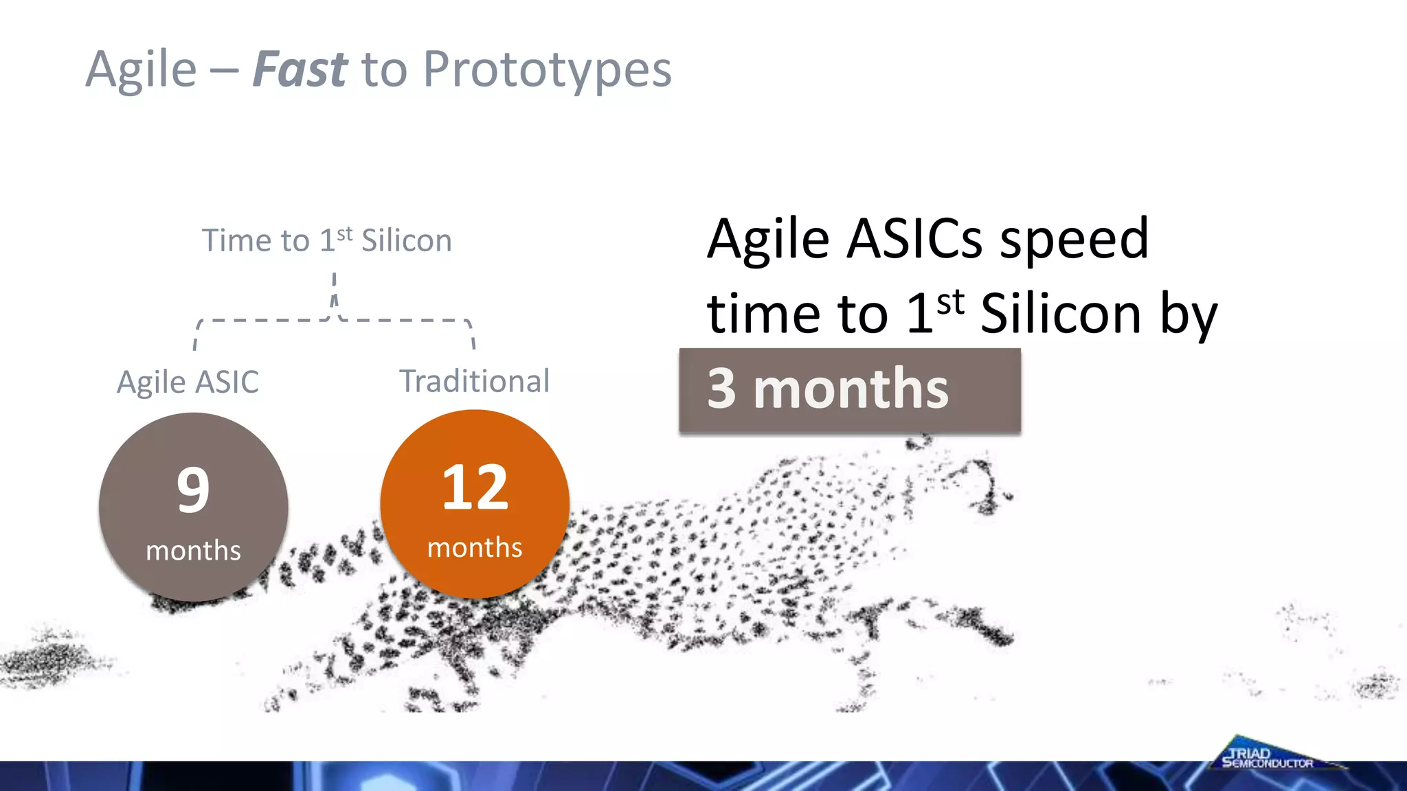
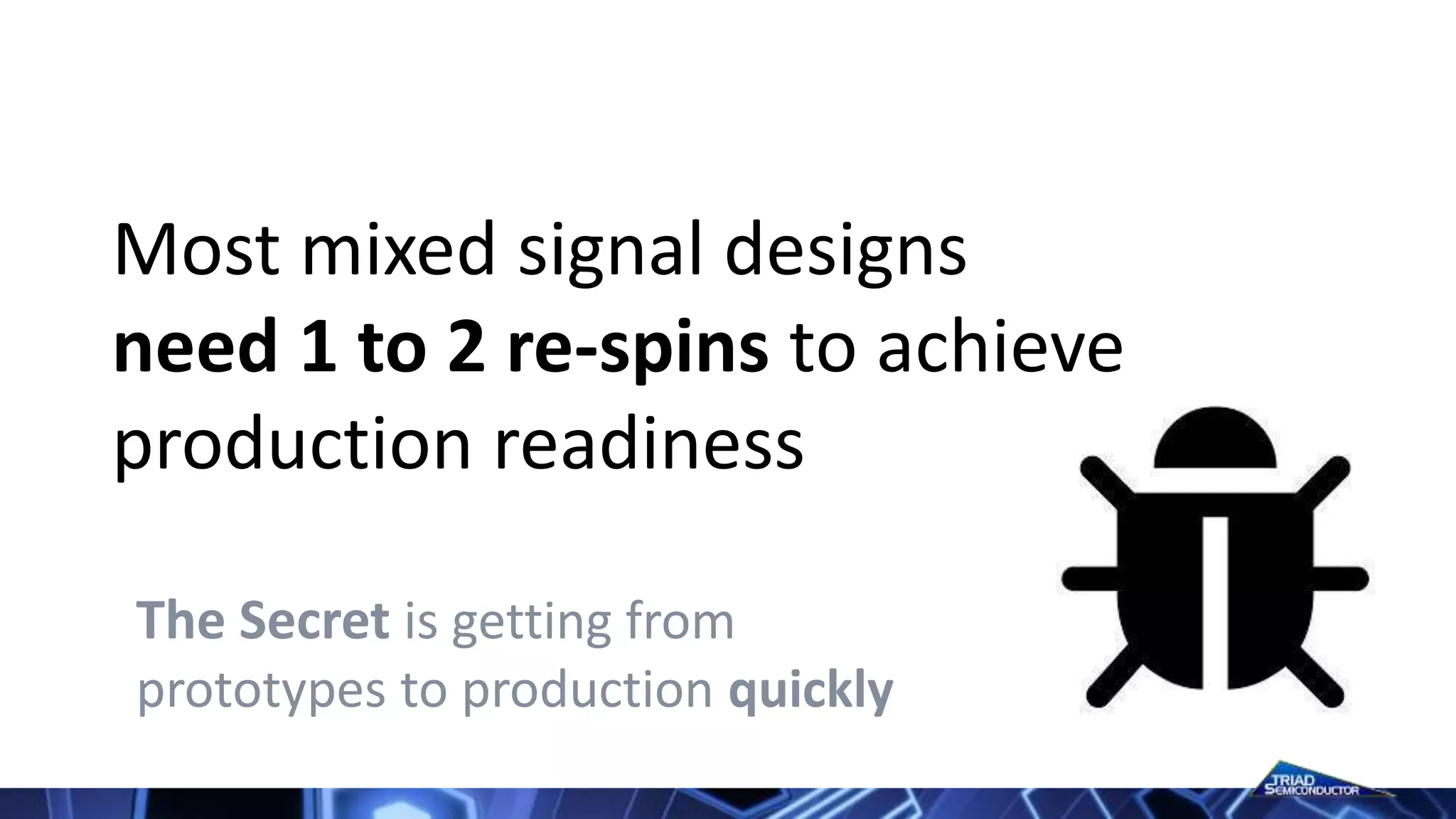
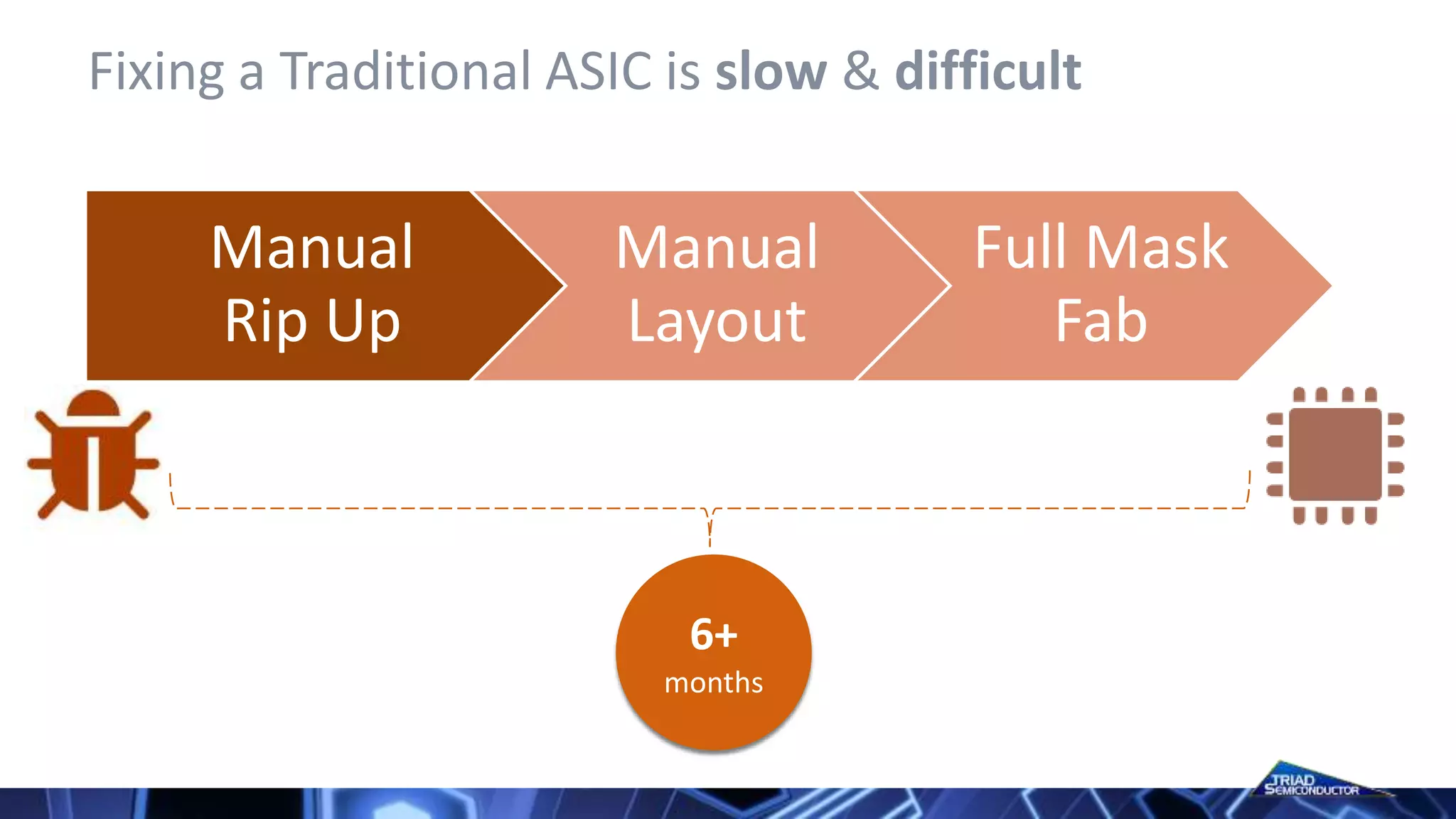

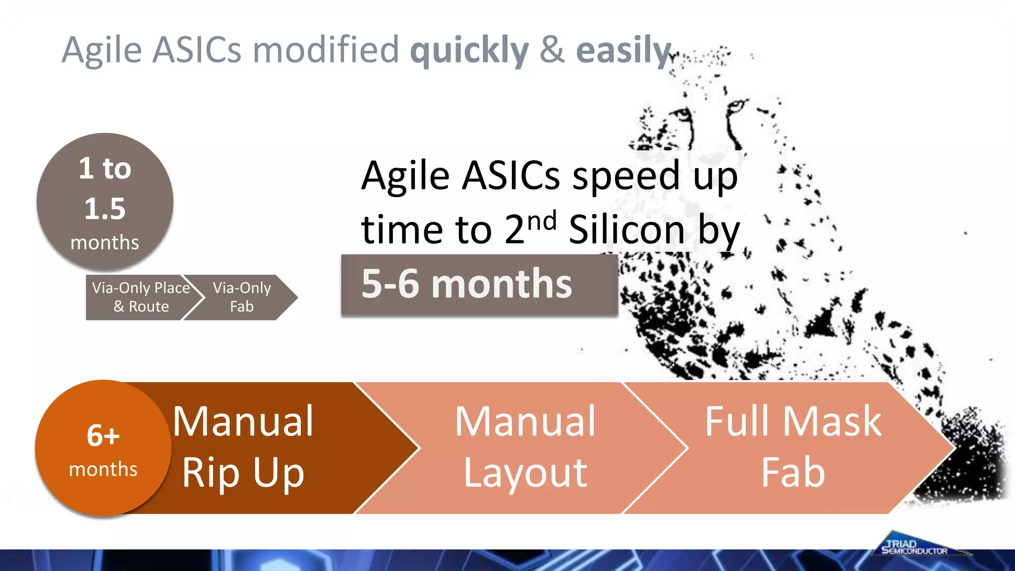

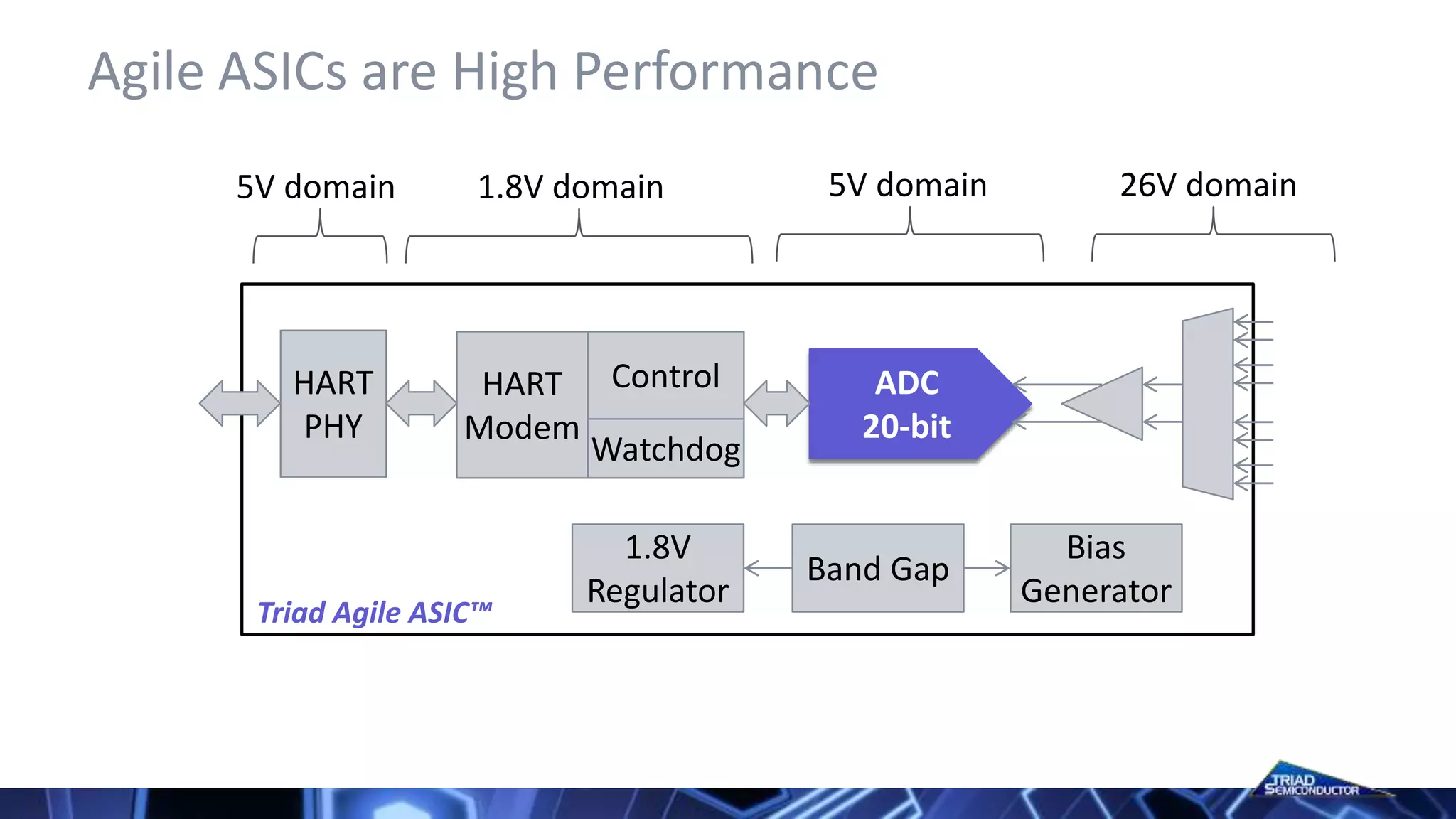
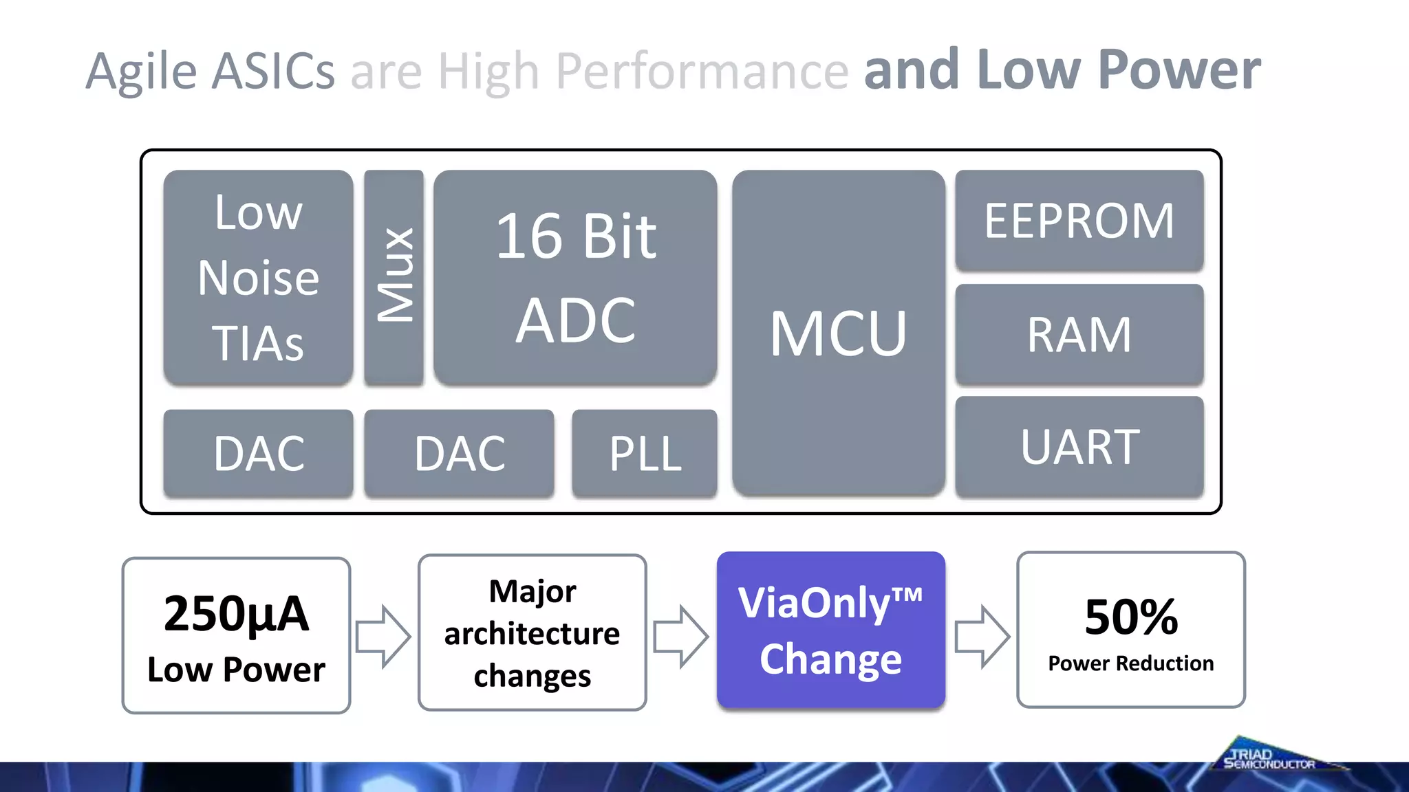
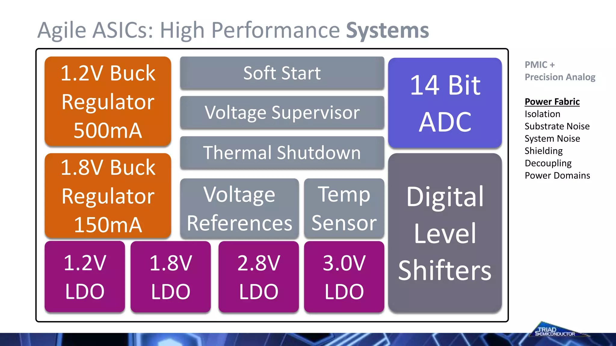
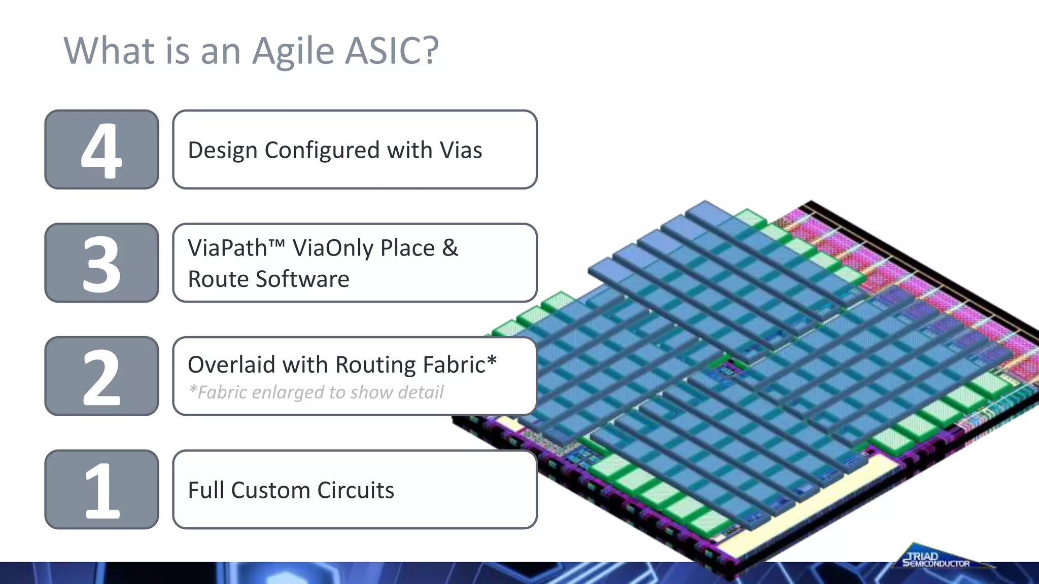
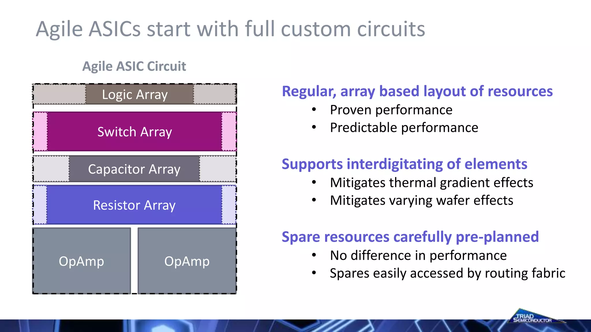
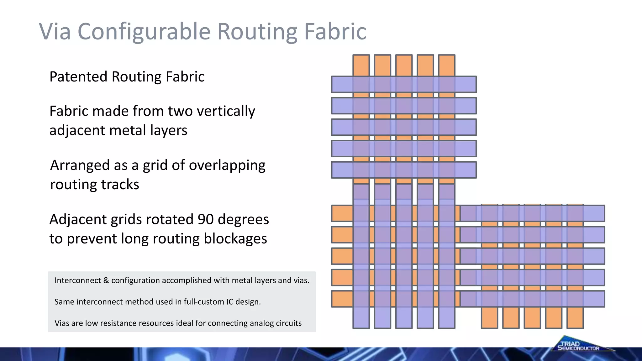
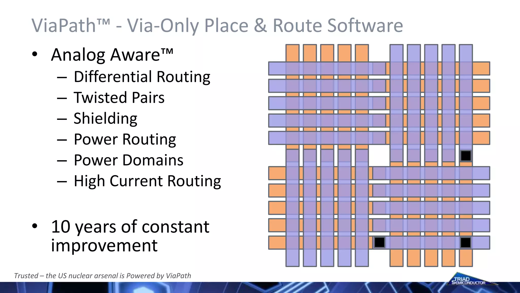
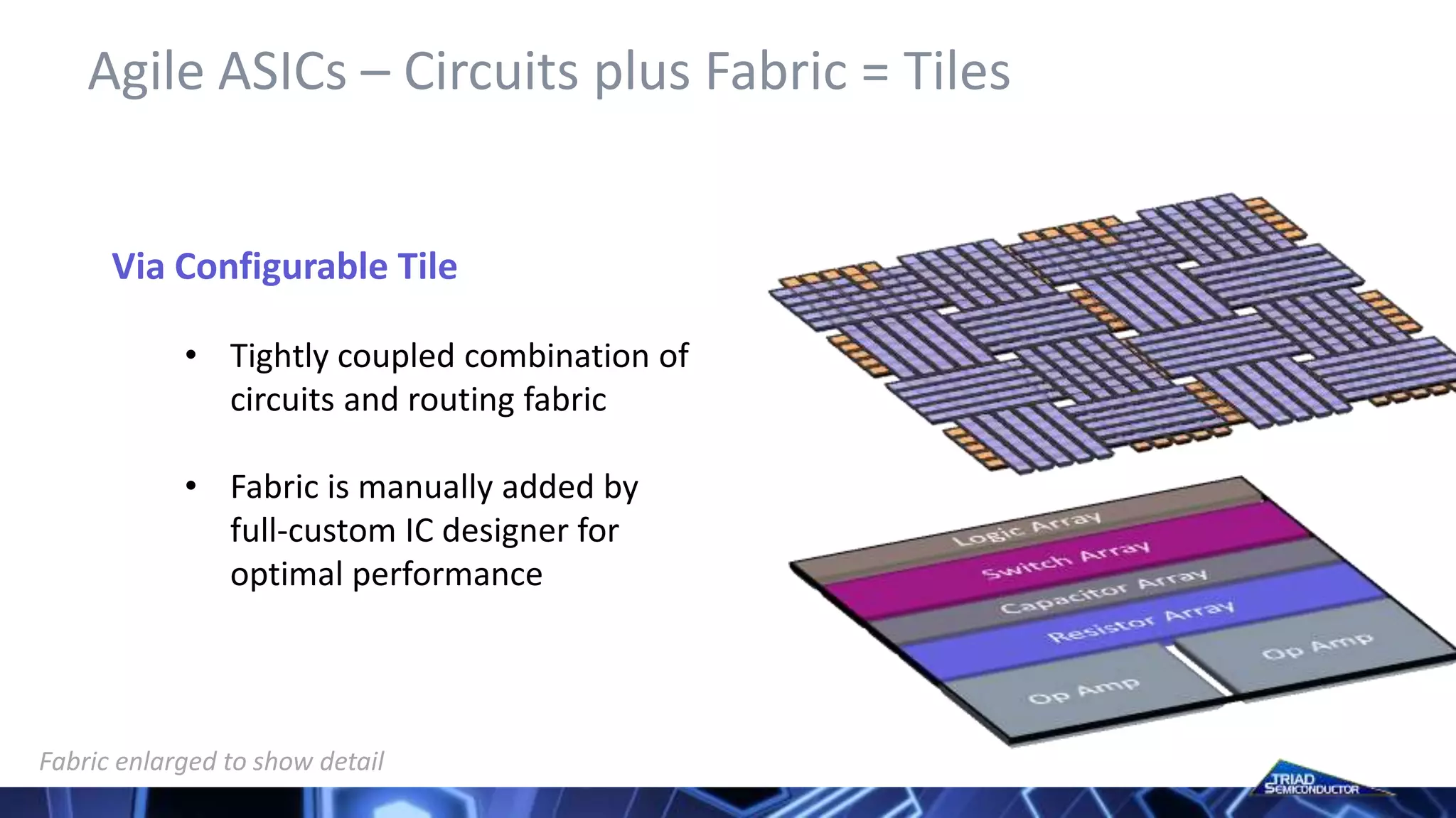
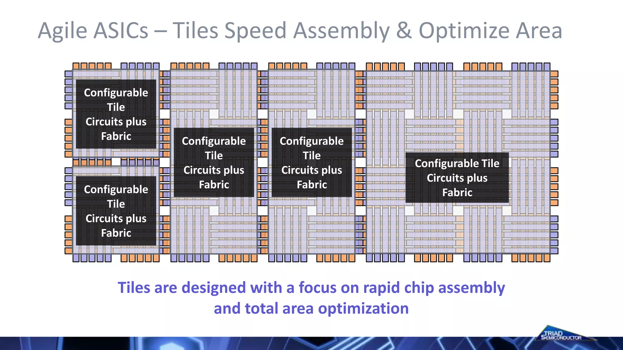
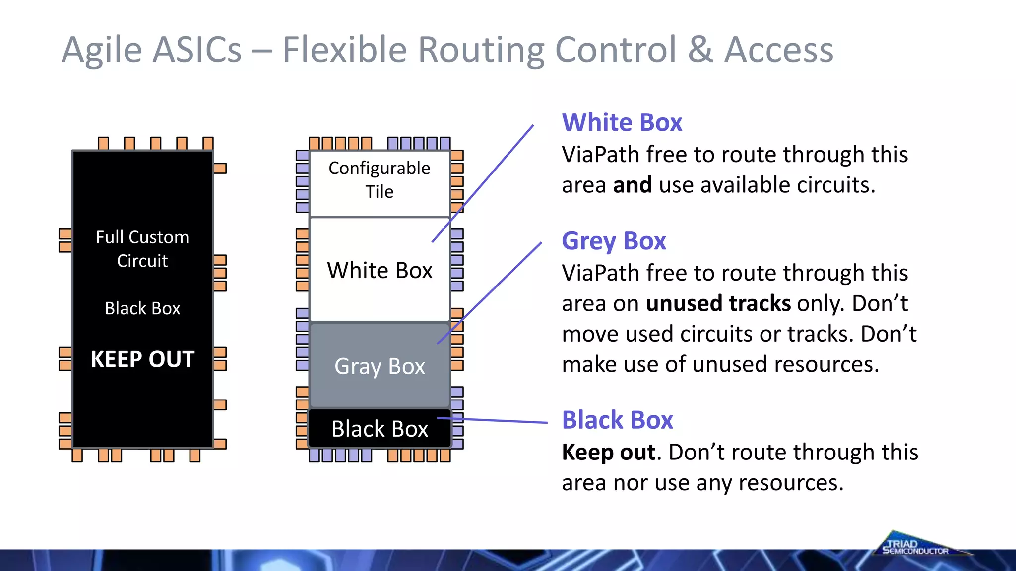
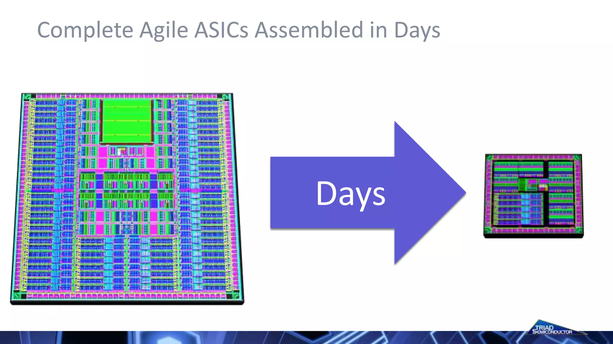
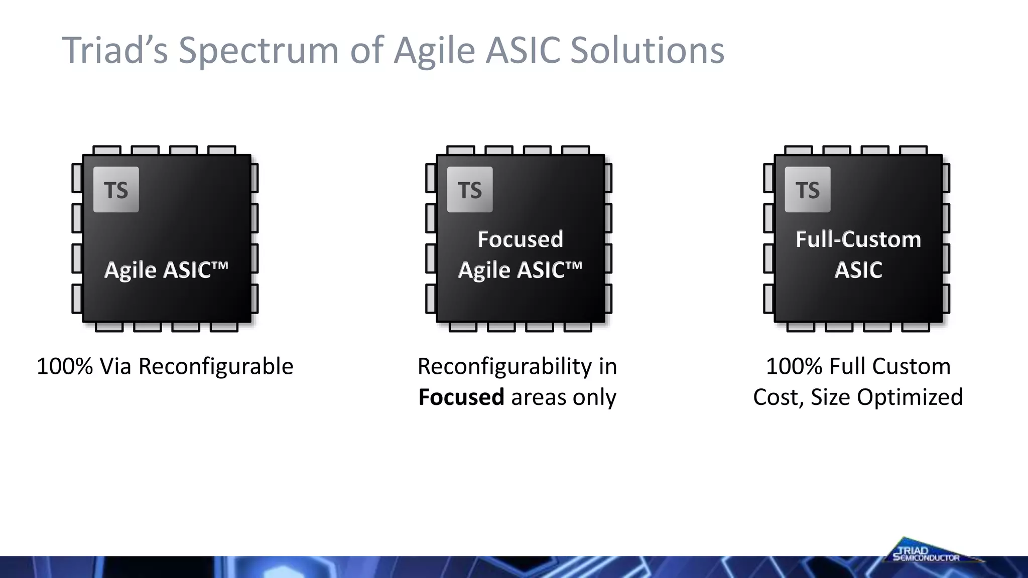
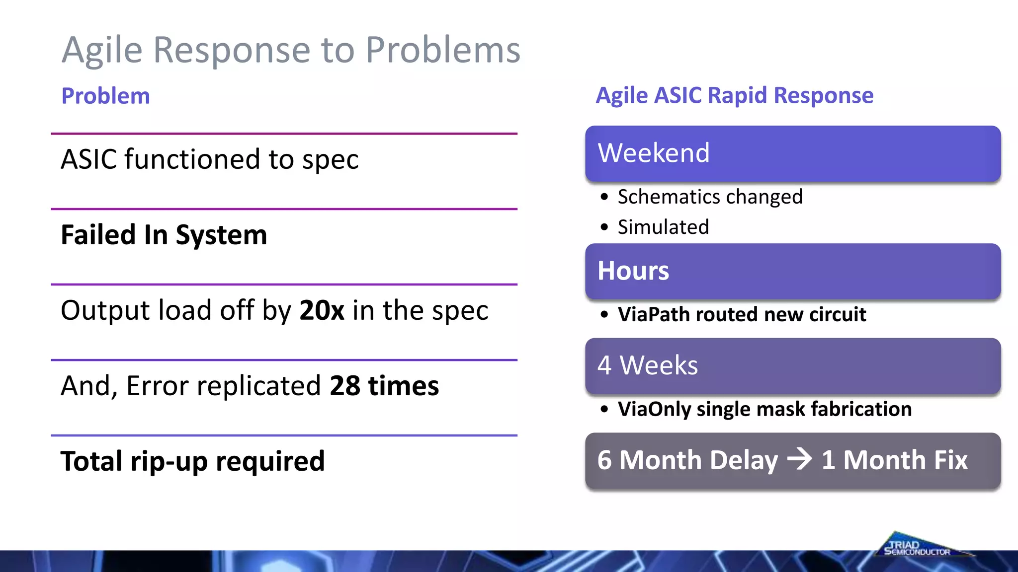
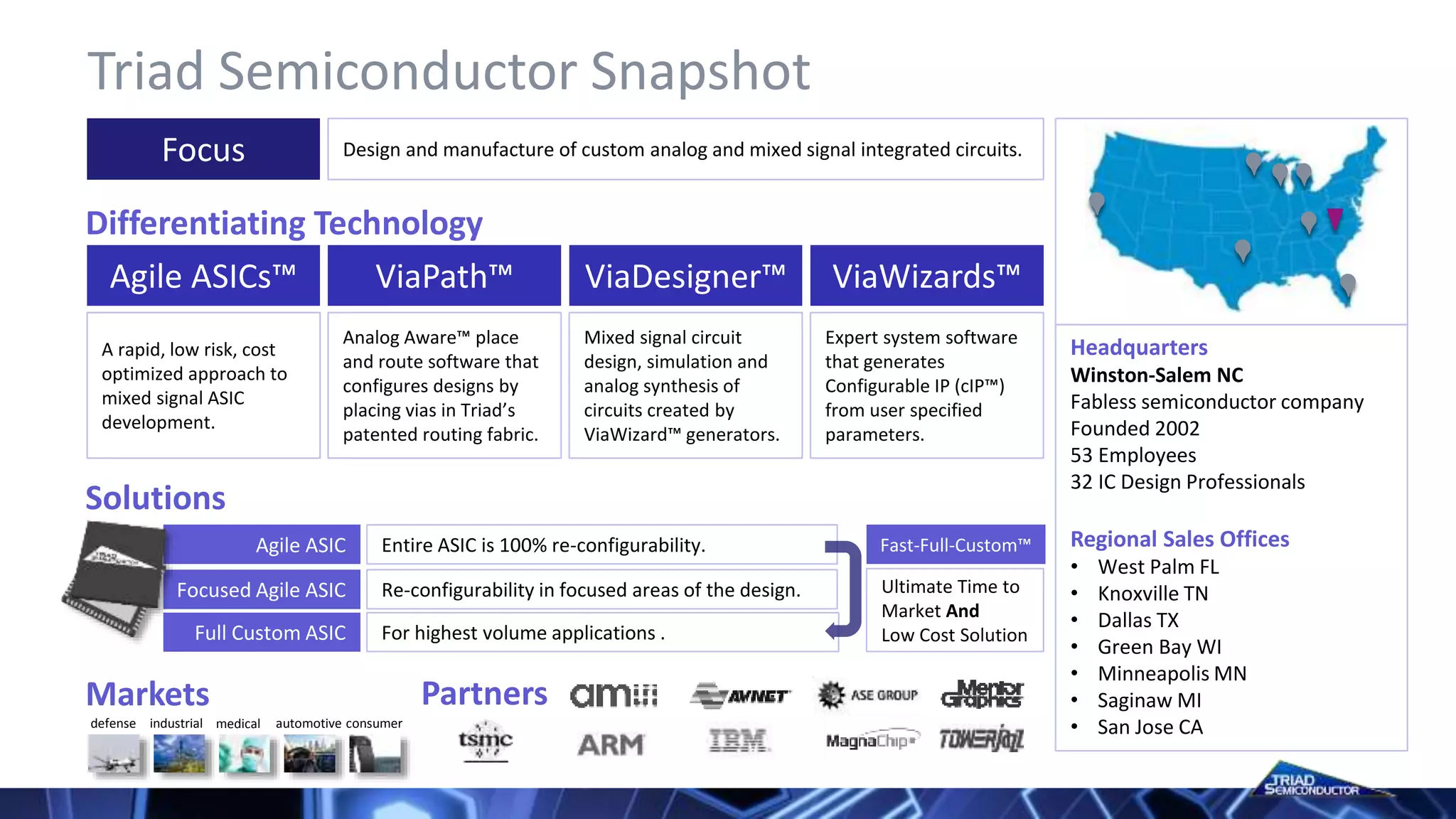

Triad Semiconductor provides analog and mixed signal ASIC design and manufacturing solutions using its Agile ASICTM approach. The Agile ASIC approach combines full custom analog circuits with a configurable routing fabric that allows designs to be rapidly modified using a via-only mask set. This enables designs to go from prototypes to production quickly and respond rapidly to changes or issues, speeding development times. Triad has expertise in markets like defense, industrial, medical, automotive, and consumer.