Downloaded 120 times
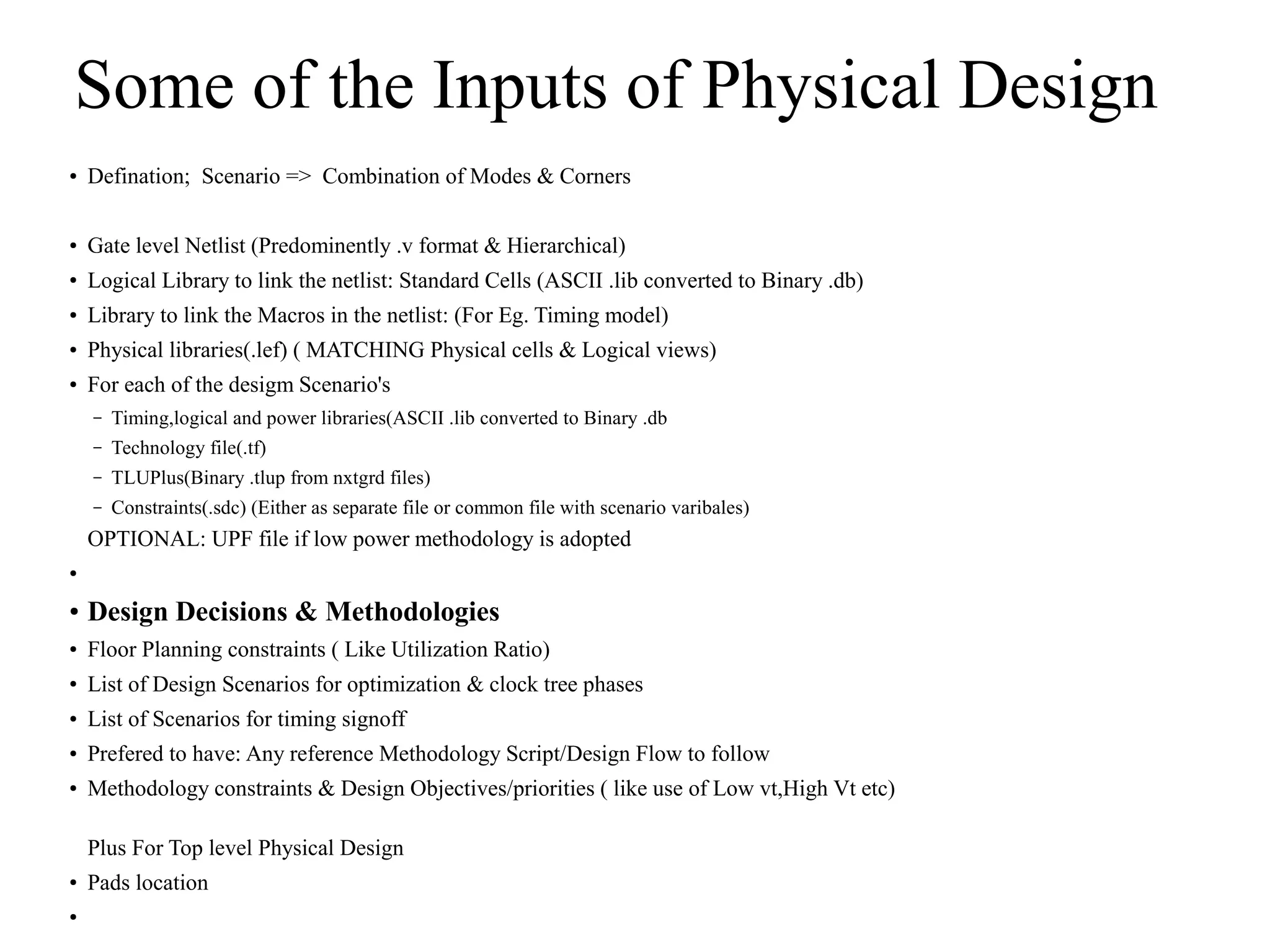


This document discusses the key inputs required for the physical design phase of a VLSI chip, using Synopsys tools as an example. The main inputs are: (1) a gate-level netlist describing the logical connections, (2) libraries providing timing, power and physical information for standard cells and macros, (3) a technology file describing manufacturing details, (4) parasitic extraction files (TLU+) for timing analysis, and (5) constraints describing design objectives. Additional inputs include floorplanning guidelines, scenarios for optimization, and reference design methodologies. The goal of physical design is to implement the logic from the netlist while meeting area, timing and power targets.
Introduction to VLSI Physical Design and tools used (Synopsys) by A.Sai Kishore.
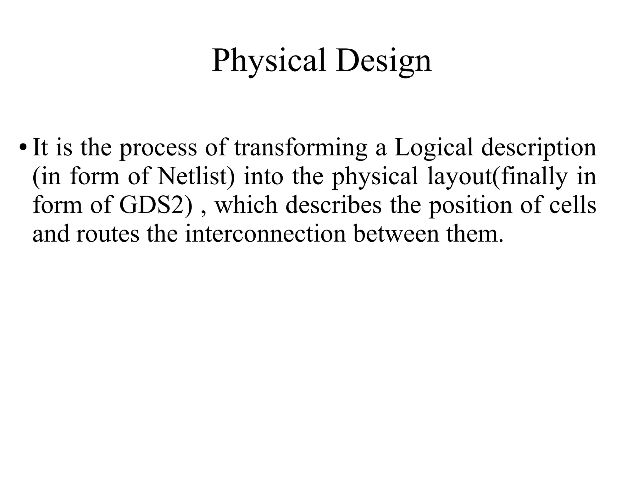
Transformation of logical descriptions (Netlist) into physical layouts (GDS2) for VLSI.
Details on various inputs for Physical Design including netlists, libraries, constraints, and design scenarios.
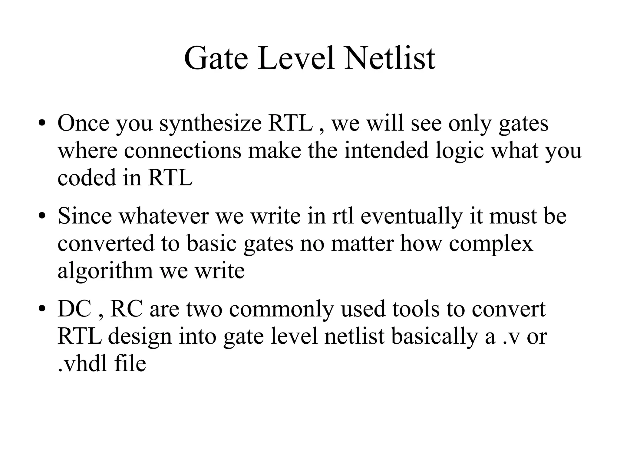
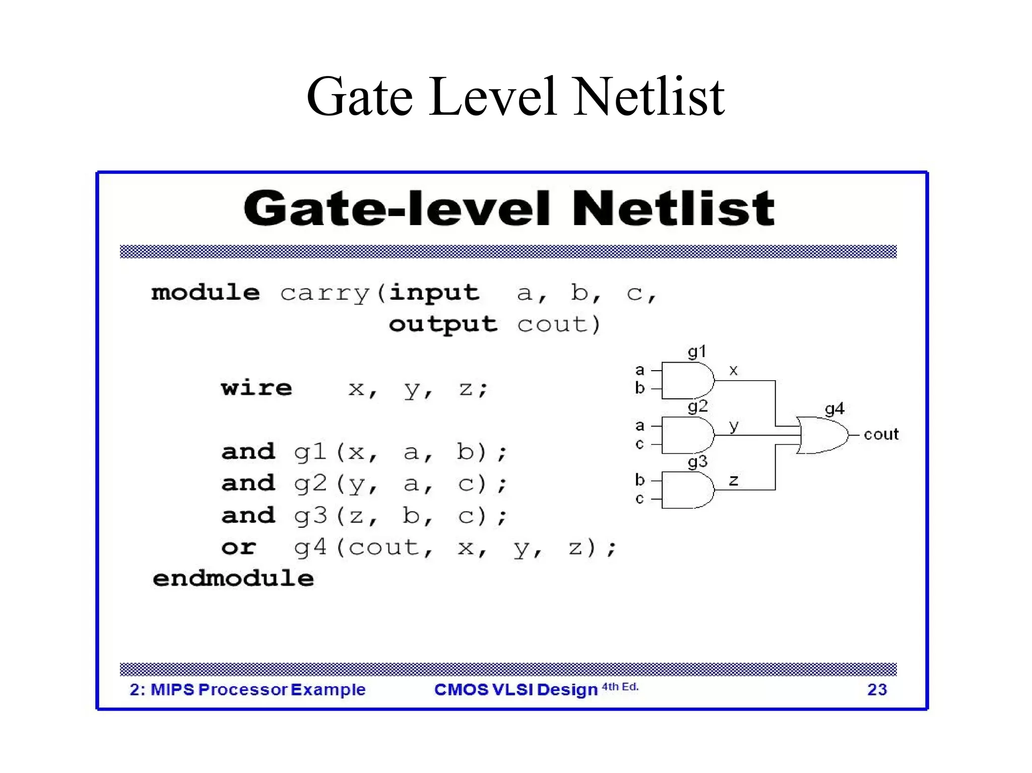
Overview of gate level netlist, synthesized from RTL to basic gates, using tools like DC and RC.
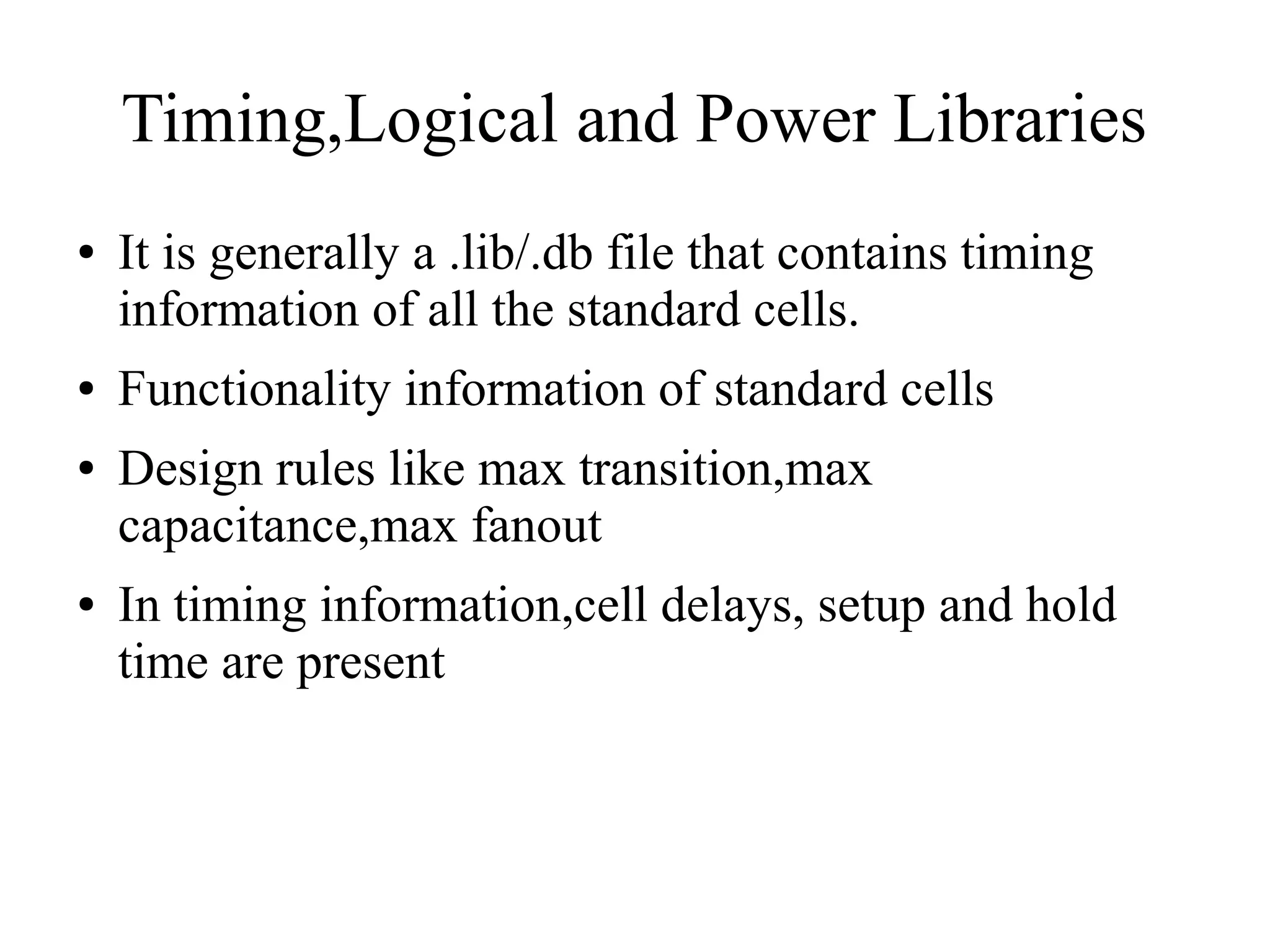
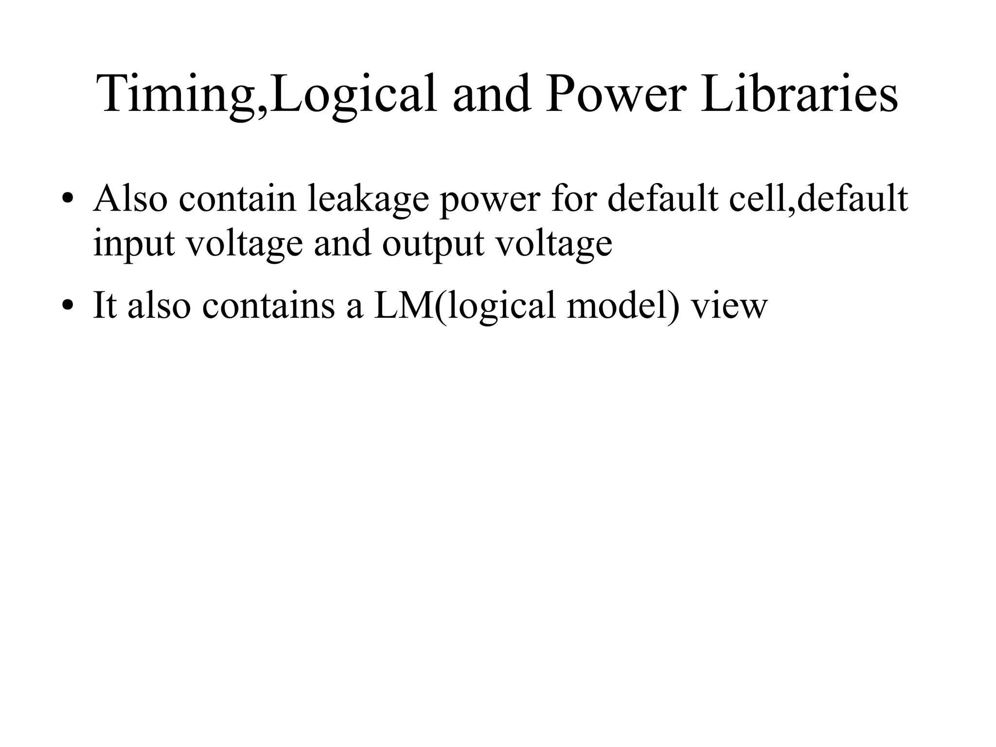
Timing, logical, and power libraries containing cell delays, design rules, and leakage power details.
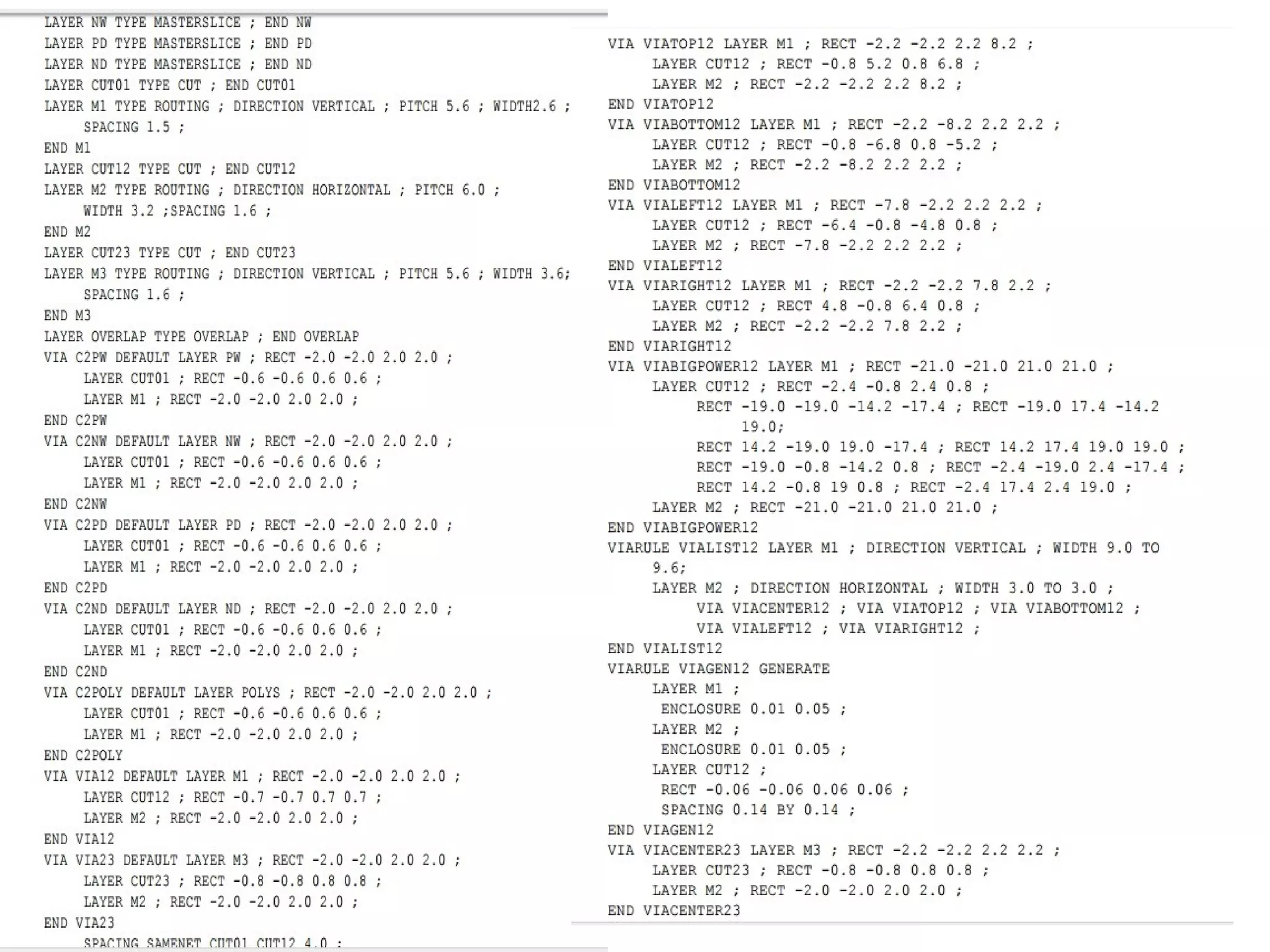
Description of physical libraries (.lef) containing cell info, routing directions, and details for tapeout.
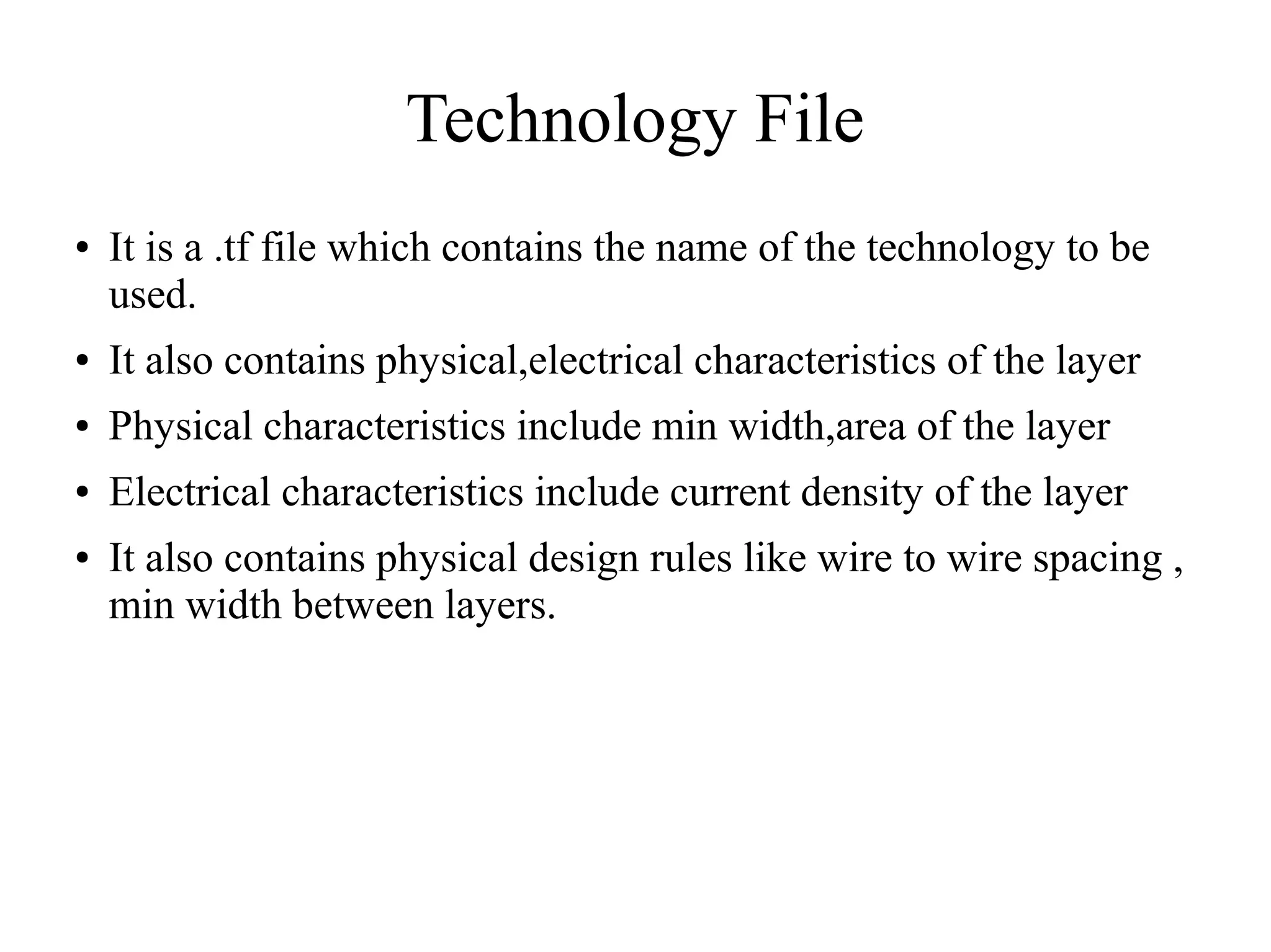
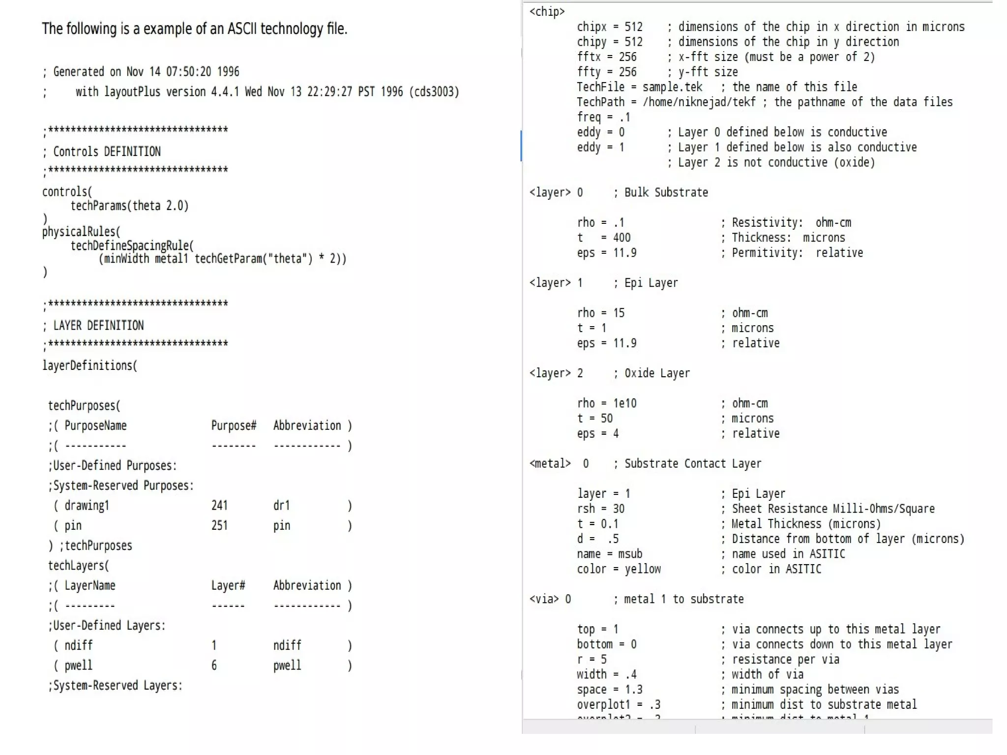
Description of technology files (.tf) which includes physical and electrical characteristics of layers.
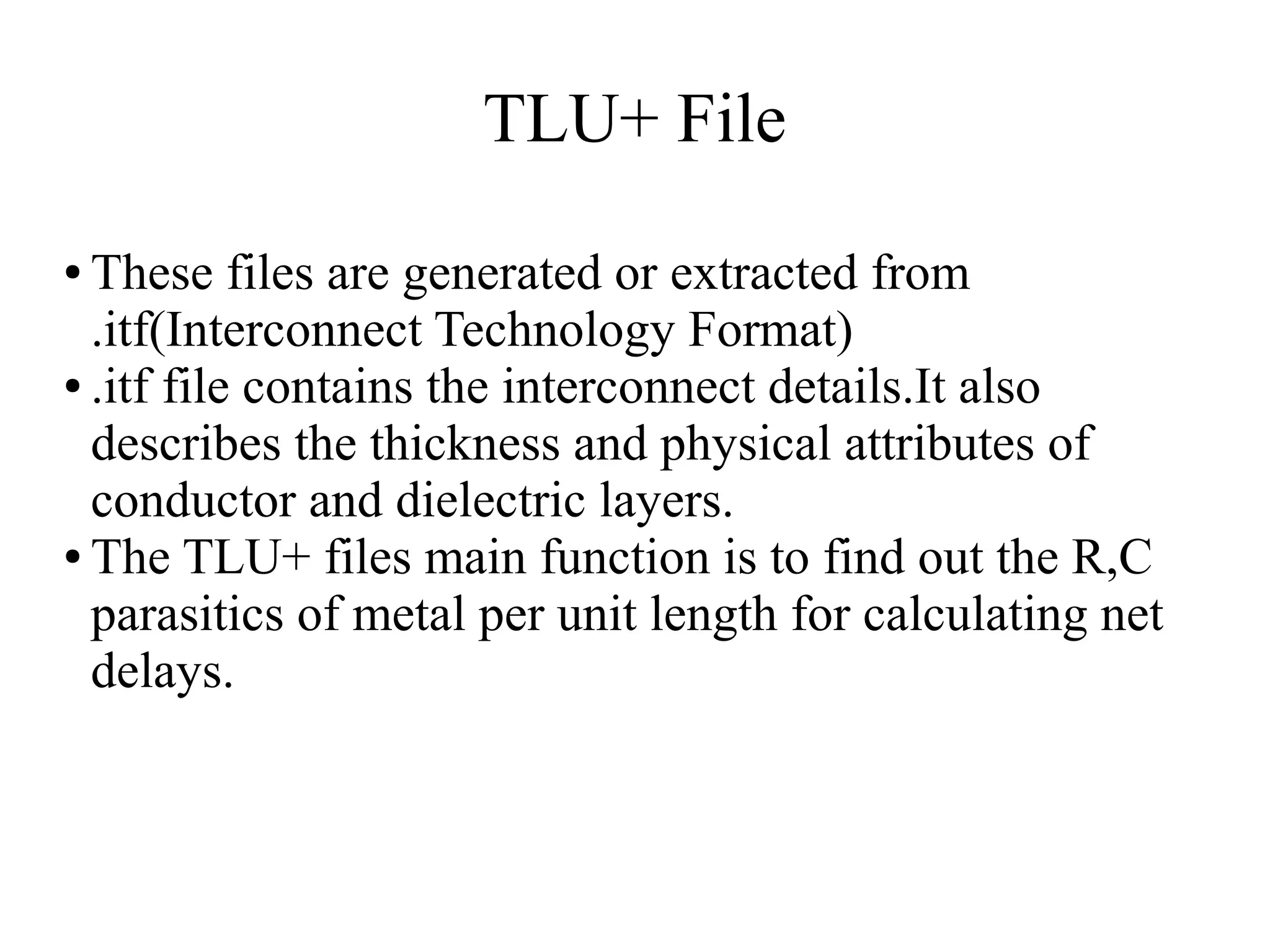
TLU+ files generated from .itf provide R,C parasitics data needed for net delay calculations.
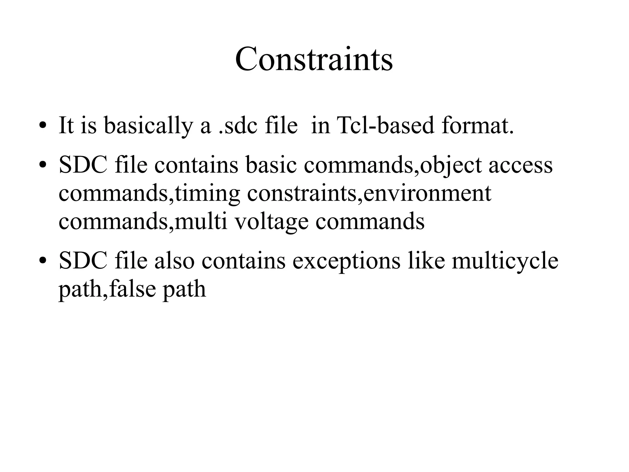
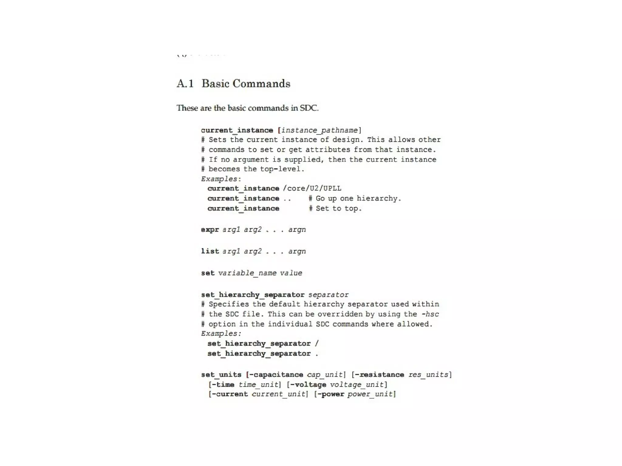
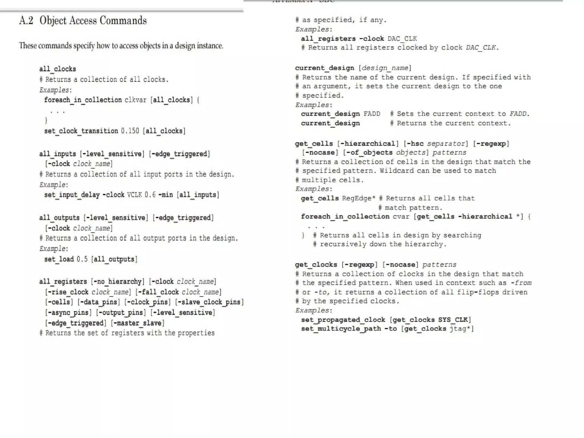
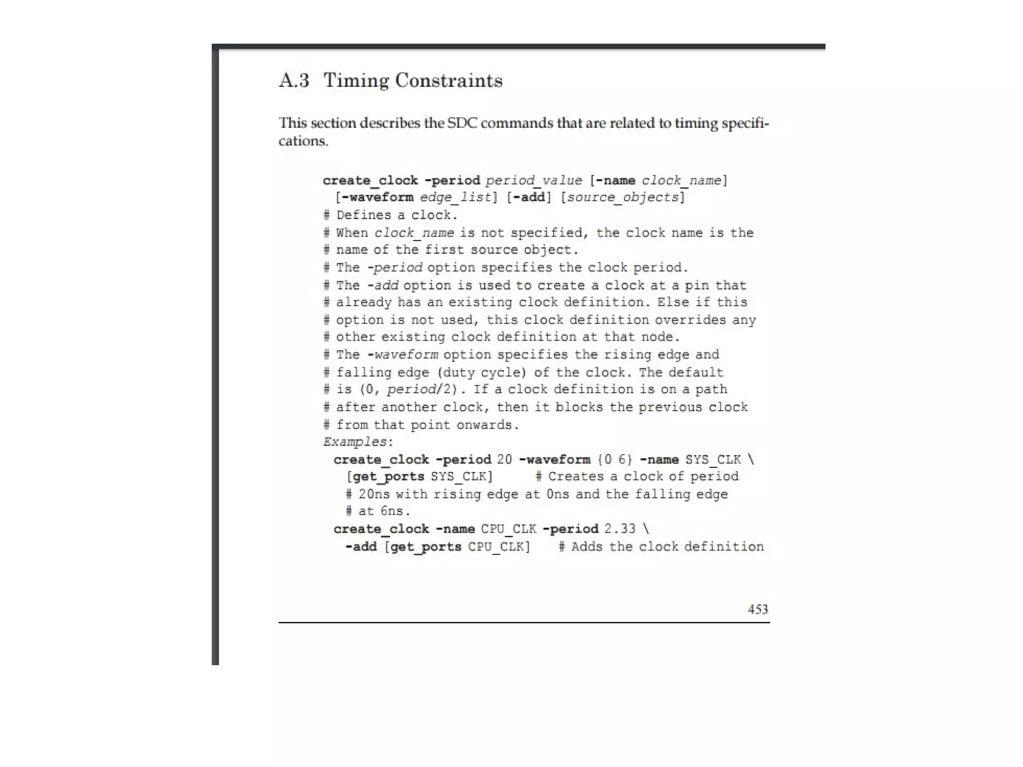
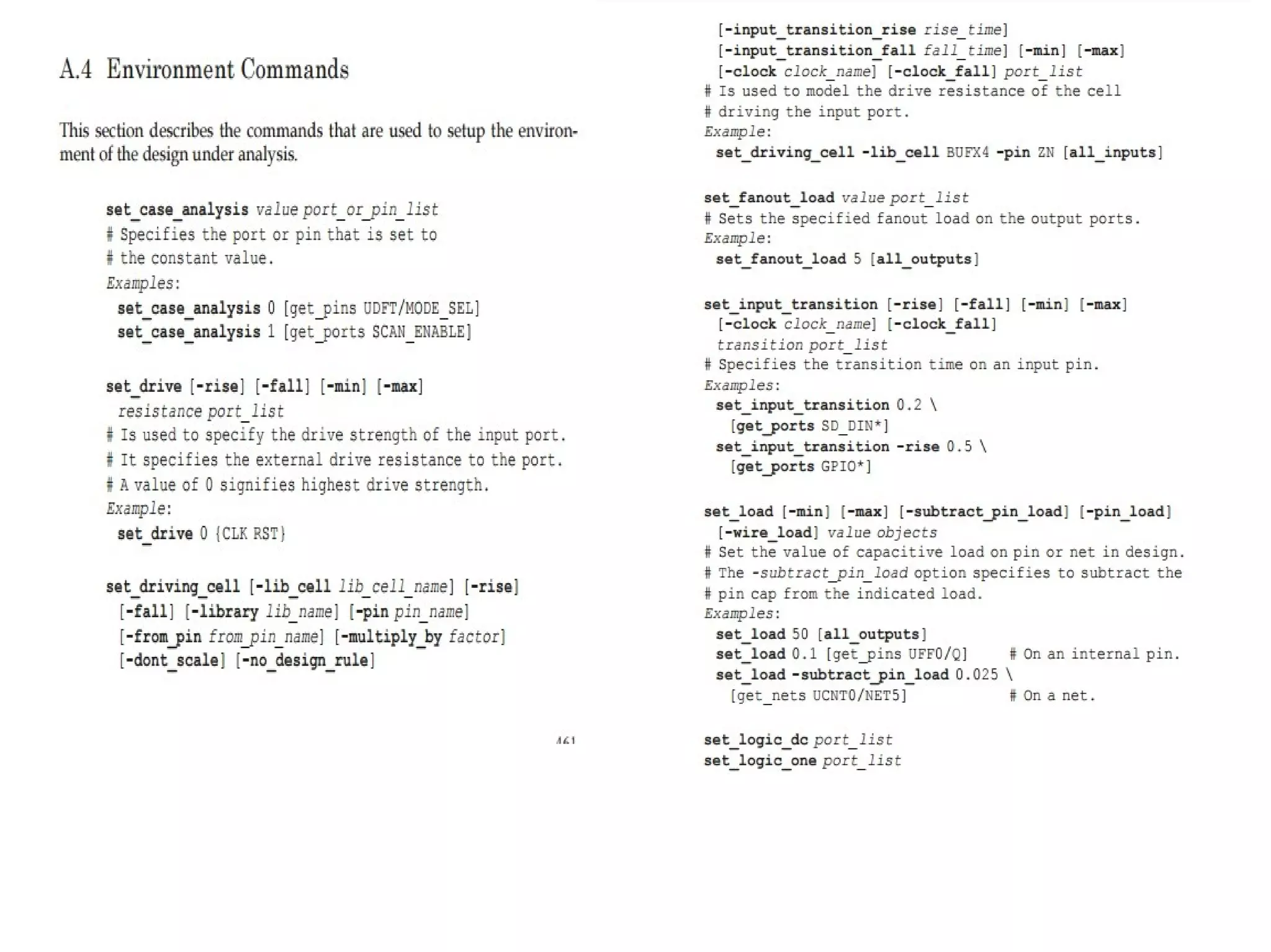
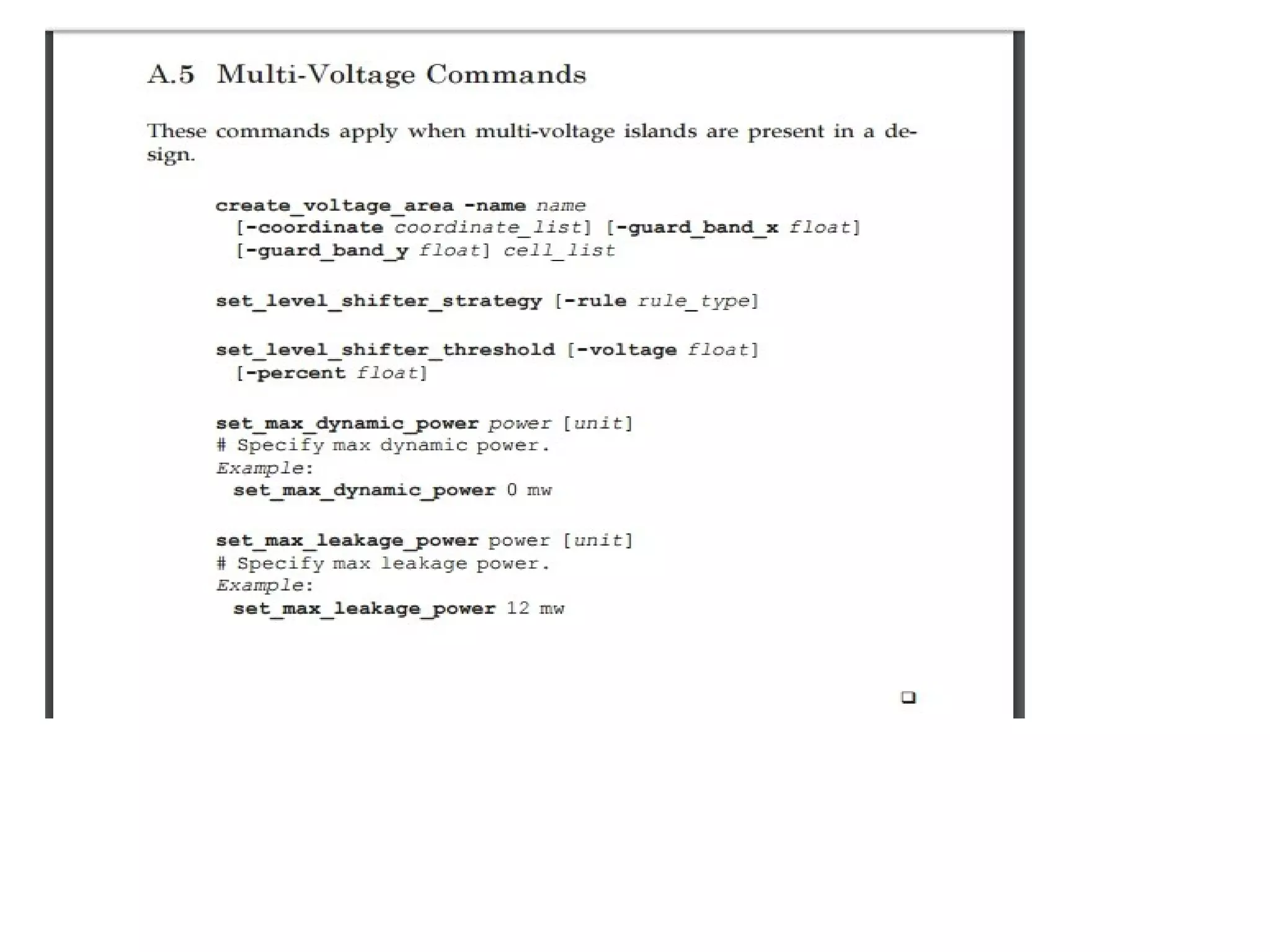
SDC file structure in Tcl format for timing constraints, commands, and exceptions in design.
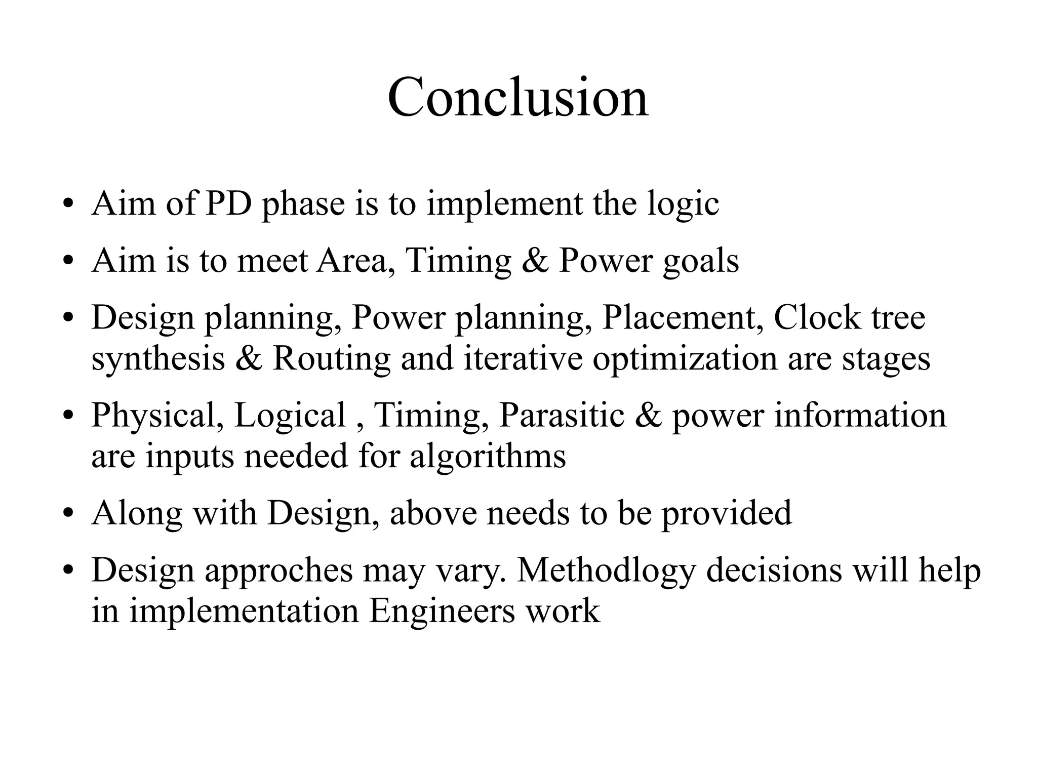
Summary of the Physical Design phase goals including area, timing, and power objectives, and methodologies.


![ANPARA THERMAL POWER STATION[1] sangam.pdf](https://cdn.slidesharecdn.com/ss_thumbnails/anparathermalpowerstation1sangam-251121115219-9261cde4-thumbnail.jpg?width=640&height=640&fit=bounds)


