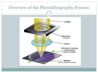
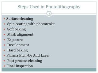
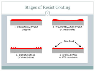
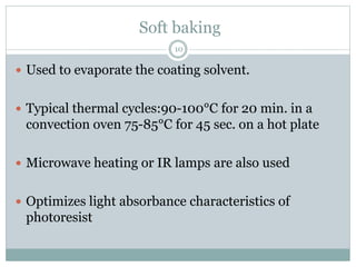
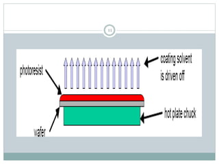
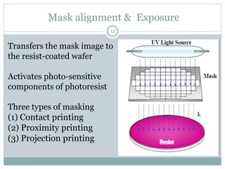
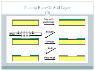
Lithography Fabrication
1
Jadhav Avinash J
 2K13E11
 Savitri Bai Phule Pune University
What is Lithography?
 Lithography(Greek word) means printing is done
on stone.
 Photo-litho-graphy: light-silicon wafer-printing.
 Components in photolithography:
(1)Mask (2)Photoresist (3)UV exposure system
2
Overview of the Photolithography Process
3
Steps Used in Photolithography
 Surface cleaning
 Spin coating with photoresist
 Soft baking
 Mask alignment
 Exposure
 Development
 Hard baking
 Plasma Etch-Or Add Layer
 Post process cleaning
 Final Inspection
4
Surface Cleaning
 Typical contaminants that must be removed prior to
photoresist coating: dust from scribing or cleaving
(minimized by laser scribing)
 photoresist residue from previous photolithography
(minimized by performing oxygen plasma ashing)
 atmospheric dust (minimized by good clean room
practice)
 bacteria (minimized by good DI water system)
5
6
 films from other sources:
-solvent residue
-H2 O residue
-photoresist or developer residue
-silicone
 For particularly troublesome grease, oil, or wax
stains: Start with 2-5 min. soak in 1,1,1-
trichloroethane (TCA) or trichloroethylene (TCE)
with ultrasonic agitation prior to acetone
Spin coating with photoresist
 Wafer is held on a spinner chuck by vacuum and
resist is coated to uniform thickness by spin coating.
 Typically 3000 - 6000 rpm for 15-30 seconds.
 Resist thickness is set by: primarily resist viscosity
secondarily spinner rotational speed
 Most resist thicknesses are 1-2 μm for commercial Si
processes.
7
8
 Resist thickness is given by
t =square of( kp)/root of(w1),
where,
k = spinner constant, typically 80-100
p = resist solids content in percent
w = spinner rotational speed in rpm/1000
Stages of Resist Coating
9
Soft baking
 Used to evaporate the coating solvent.
 Typical thermal cycles:90-100°C for 20 min. in a
convection oven 75-85°C for 45 sec. on a hot plate
 Microwave heating or IR lamps are also used
 Optimizes light absorbance characteristics of
photoresist
10
11
Mask alignment & Exposure
12
Transfers the mask image to
the resist-coated wafer
Activates photo-sensitive
components of photoresist
Three types of masking
(1) Contact printing
(2) Proximity printing
(3) Projection printing
13
14
 Contact printing capable of high resolution but has
unacceptable defect densities. May be used in
Development but not manufacturing.
 Proximity printing cannot easily print features below
a few mm in line width. Used in nano-technolgy.
 Projection printing provides high resolution and low
defect densities and dominates today.They print » 50
wafers/hour.
Positive resist & Negative resist
15
Development
16
 Soluble areas of photoresist are dissolved by
developer chemical
 Visible patterns appear on wafer
 Quality measures:
 –line resolution
 –uniformity
 –particles & defects
Hard baking
17
 Used to stabilize and harden the developed
photoresist prior to processing steps that the resist
will mask.
 Postbake removes any remaining traces of the
coating solvent or developer.
 Higher temperature than soft bake (120-150 degree)
Plasma Etch-Or Add Layer
18
Post process cleaning
19
 Plasma etching with O2 (ashing)
 Simple solvents are generally sufficient for non-
postbaked photoresists:
 Positive photoresists:
aceton
trichloroethylene (TCE)
 Negative photoresists:
methyl ethyl ketone
methyl isobutyl ketone

Final Inspection
20
 Photoresist has been completely removed
 Pattern on wafer matches mask pattern (positive
resist)
 Quality issues:
–defects
–particles
–step height
–critical dimensions
Any Questions???
21

lithographyfabrication-141013020209-conversion-gate02.pdf

  • 1.
    Lithography Fabrication 1 Jadhav AvinashJ  2K13E11  Savitri Bai Phule Pune University
  • 2.
    What is Lithography? Lithography(Greek word) means printing is done on stone.  Photo-litho-graphy: light-silicon wafer-printing.  Components in photolithography: (1)Mask (2)Photoresist (3)UV exposure system 2
  • 3.
    Overview of thePhotolithography Process 3
  • 4.
    Steps Used inPhotolithography  Surface cleaning  Spin coating with photoresist  Soft baking  Mask alignment  Exposure  Development  Hard baking  Plasma Etch-Or Add Layer  Post process cleaning  Final Inspection 4
  • 5.
    Surface Cleaning  Typicalcontaminants that must be removed prior to photoresist coating: dust from scribing or cleaving (minimized by laser scribing)  photoresist residue from previous photolithography (minimized by performing oxygen plasma ashing)  atmospheric dust (minimized by good clean room practice)  bacteria (minimized by good DI water system) 5
  • 6.
    6  films fromother sources: -solvent residue -H2 O residue -photoresist or developer residue -silicone  For particularly troublesome grease, oil, or wax stains: Start with 2-5 min. soak in 1,1,1- trichloroethane (TCA) or trichloroethylene (TCE) with ultrasonic agitation prior to acetone
  • 7.
    Spin coating withphotoresist  Wafer is held on a spinner chuck by vacuum and resist is coated to uniform thickness by spin coating.  Typically 3000 - 6000 rpm for 15-30 seconds.  Resist thickness is set by: primarily resist viscosity secondarily spinner rotational speed  Most resist thicknesses are 1-2 μm for commercial Si processes. 7
  • 8.
    8  Resist thicknessis given by t =square of( kp)/root of(w1), where, k = spinner constant, typically 80-100 p = resist solids content in percent w = spinner rotational speed in rpm/1000
  • 9.
  • 10.
    Soft baking  Usedto evaporate the coating solvent.  Typical thermal cycles:90-100°C for 20 min. in a convection oven 75-85°C for 45 sec. on a hot plate  Microwave heating or IR lamps are also used  Optimizes light absorbance characteristics of photoresist 10
  • 11.
  • 12.
    Mask alignment &Exposure 12 Transfers the mask image to the resist-coated wafer Activates photo-sensitive components of photoresist Three types of masking (1) Contact printing (2) Proximity printing (3) Projection printing
  • 13.
  • 14.
    14  Contact printingcapable of high resolution but has unacceptable defect densities. May be used in Development but not manufacturing.  Proximity printing cannot easily print features below a few mm in line width. Used in nano-technolgy.  Projection printing provides high resolution and low defect densities and dominates today.They print » 50 wafers/hour.
  • 15.
    Positive resist &Negative resist 15
  • 16.
    Development 16  Soluble areasof photoresist are dissolved by developer chemical  Visible patterns appear on wafer  Quality measures:  –line resolution  –uniformity  –particles & defects
  • 17.
    Hard baking 17  Usedto stabilize and harden the developed photoresist prior to processing steps that the resist will mask.  Postbake removes any remaining traces of the coating solvent or developer.  Higher temperature than soft bake (120-150 degree)
  • 18.
  • 19.
    Post process cleaning 19 Plasma etching with O2 (ashing)  Simple solvents are generally sufficient for non- postbaked photoresists:  Positive photoresists: aceton trichloroethylene (TCE)  Negative photoresists: methyl ethyl ketone methyl isobutyl ketone 
  • 20.
    Final Inspection 20  Photoresisthas been completely removed  Pattern on wafer matches mask pattern (positive resist)  Quality issues: –defects –particles –step height –critical dimensions
  • 21.