Downloaded 163 times


![13Microelectronics Processing Course - J. Salzman - Jan. 2002
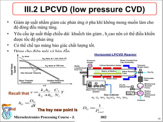
CVD kinetic growth model-IICVD kinetic growth model-II
We can now express the growth rate of the silicon film by writing
where N1
is the number of silicon atoms incorporated into a unit volume of the film.
Its value for silicon is 5.0×10²²
cm-3
. Noting that CG
= YCT
where CT
is the total
number of molecules per cubic centimeter in the gas, we get the expression for the
growth rate,
11 N
C
hk
hk
N
F
v G
GS
GS
+
==
Y
N
C
hk
hk
N
F
v T
GS
GS
11 +
==
The growth rate at a given mole fraction is determined by the smaller of hG
or kS
. In
the limiting cases the growth rate will be given either by
[surface-reaction control]
or by
[mass-transfer control].Yk
N
C
v S
T
1
≅
Yk
N
C
v S
T
1
≅
hGY](https://image.slidesharecdn.com/cvd-150112003247-conversion-gate02/85/Cvd-13-320.jpg)


The document discusses chemical vapor deposition (CVD) processes for thin film deposition in microelectronics processing. CVD involves depositing a thin solid film on a substrate through chemical reactions of vapor phase precursors. Key aspects covered include common CVD systems like atmospheric pressure CVD, low pressure CVD, and plasma enhanced CVD. The document also examines the CVD kinetic growth model, factors that influence the growth rate like mass transfer and surface reactions, examples of CVD films like silicon nitride and polysilicon, and steps in the CVD process.


