Download to read offline
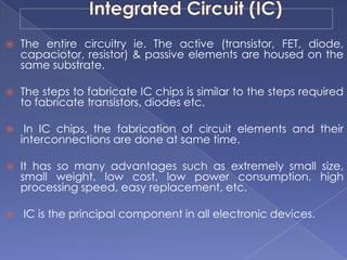
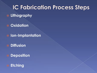
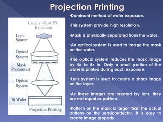

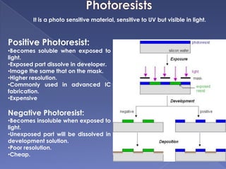

The document describes the process of fabricating integrated circuit (IC) chips. There are several key steps: lithography is used to transfer circuit patterns onto silicon wafers through photomasks, and oxidation, deposition, ion implantation, and etching are carried out to build up the transistor layers. Projection lithography is the dominant exposure method and involves projecting a reduced image of the photomask onto the wafer through a lens system to achieve high resolution needed for modern chips. Positive photoresist is commonly used and becomes soluble when exposed to light, allowing developed areas to be etched. The fabrication process layers and patterns all the necessary circuit elements and interconnects on a single substrate to produce an operational IC.


![Thin_Film_Technology_introduction[1]](https://cdn.slidesharecdn.com/ss_thumbnails/1b4496c8-2102-411b-8465-a3dd3f398327-150205034538-conversion-gate02-thumbnail.jpg?width=640&height=640&fit=bounds)


