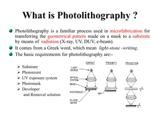
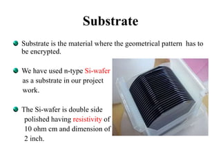
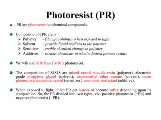
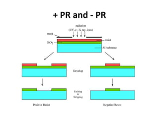
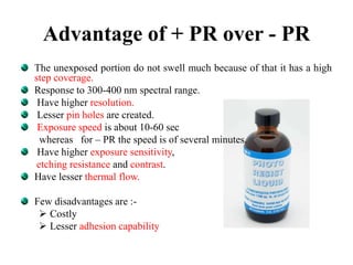
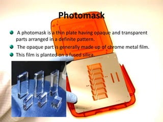
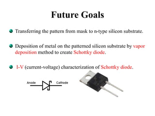
PORTABLE UV-EXPOSURE SYSTEM FOR
OPTICAL MICROLITHOGRAPHY
CONTENTS
Defining Photolithography
Definition
Basic requirements in photolithography
Substrate
Photoresist
Composition of a photoresist
Positive and Negative photoresist
Advantage of Positive Resist over Negative resist
Photomask
UV exposure system
Construction and Application
Process of Photolithography
Futuristic goals
What is Photolithography ?
Photolithography is a familiar process used in microfabrication for
transferring the geometrical pattern made on a mask to a substrate
by means of radiation (X-ray, UV, DUV, e-beam).
It comes from a Greek word, which mean light-stone -writing.
The basic requirements for photolithography are:-
 Substrate
 Photoresist
 UV exposure system
 Photomask
 Developer
and Removal solution
Substrate
Substrate is the material where the geometrical pattern has to
be encrypted.
We have used n-type Si-wafer
as a substrate in our project
work.
The Si-wafer is double side
polished having resistivity of
10 ohm cm and dimension of
2 inch.
Photoresist (PR)
PR are photosensitive chemical compounds.
Composition of PR are :-
 Polymer - Change solubility when exposed to light
 Solvent - provide liquid medium to the polymer
 Sensitizer - enable chemical change in polymer
 Additives - various chemicals to obtain desired process results
We will use S1818 and S1813 photoresist.
The composition of S1818 are mixed cresol novolak resin (polymer), electronic
grade propylene glycol (solvent), monomethyl ether acetate (solvent), diazo
photoactive compound cresol (sensitizer), non-ionic Surfactant (additive).
When exposed to light, either PR get harder or become softer depending upon its
composition. So, the PR divided into two types, viz- positive photoresist (+PR) and
negative photoresist (- PR).
+ PR and - PR
Advantage of + PR over - PR
The unexposed portion do not swell much because of that it has a high
step coverage.
Response to 300-400 nm spectral range.
Have higher resolution.
Lesser pin holes are created.
Exposure speed is about 10-60 sec
whereas for – PR the speed is of several minutes.
Have higher exposure sensitivity,
etching resistance and contrast.
Have lesser thermal flow.
Few disadvantages are :-
 Costly
 Lesser adhesion capability
Photomask
A photomask is a thin plate having opaque and transparent
parts arranged in a definite pattern.
The opaque part is generally made up of chrome metal film.
This film is planted on a fused silica.
UV Exposure System
The UV exposure system is an essential part for optical microlithography. It works
as a radiation source.
The system consists of
 An external circuit- the circuit consist of a mercury lamp, a ballast and
parallely connected capacitor.
 An cuboidal shape tin box- it has two sliders S1 and S2 .
External Circuit
The external circuit is necessary for glowing the Mercury bulb.
The circuit is shown in the figure 1.
The copper ballast is used for ignition and current limitation during
discharge and the capacitor is connected parallely for power factor
correction.
Design Of The Box
The box is of cuboidal shape
made up of tin having dimension
7 X 7 X 14.5 inch cube.
The box has two slider S1 and S2.
S1 works as a ON/OFF switch for
exposure system.
S2 is for focusing radiation on the
substrate.
Process of Photolithography
Surface Preparation
Coating
Soft baking
Alignment
Exposure
Resist Development
Hard Baking
Processing Using the Photoresist as a
masking Film (Etching)
Stripping using Removal solution
Cleaning
photoresist
silicon substrate
oxide
Ultraviolet Light
Future Goals
Transferring the pattern from mask to n-type silicon substrate.
Deposition of metal on the patterned silicon substrate by vapor
deposition method to create Schottky diode.
I-V (current-voltage) characterization of Schottky diode.
References
Mark D. Huntington;Teri W. Odom, “A portable, benchtop photolithography
system based on a solid-state light source”, SMALL 7(22):3144-
7,NOVEMBER 2011
Murat Kaya Yapici and Ilyas Farhat, “UV-LED exposure system for low cost
photolithography”, proc. Of SPIE Vol. 9052 90521T, 2014
NPTEL Lecture series at VLSI Technology by Dr. Nandita Dasgupta, IIT
MADRAS, 2009
Mod-01, Lec-15, “Schottky junction and Ohmic contacts”, NPTEL lecture by
Dr. M.R. Shenoy, IIT Delhi
Material safety data sheet, MICROPOSIT S1818 photoresist ; mod-41340 6.00
US US MSDS_US
Designing a low cost UV-Exposure System for Optical Microlithography

Designing a low cost UV-Exposure System for Optical Microlithography

  • 1.
    PORTABLE UV-EXPOSURE SYSTEMFOR OPTICAL MICROLITHOGRAPHY
  • 2.
    CONTENTS Defining Photolithography Definition Basic requirementsin photolithography Substrate Photoresist Composition of a photoresist Positive and Negative photoresist Advantage of Positive Resist over Negative resist Photomask UV exposure system Construction and Application Process of Photolithography Futuristic goals
  • 4.
    What is Photolithography? Photolithography is a familiar process used in microfabrication for transferring the geometrical pattern made on a mask to a substrate by means of radiation (X-ray, UV, DUV, e-beam). It comes from a Greek word, which mean light-stone -writing. The basic requirements for photolithography are:-  Substrate  Photoresist  UV exposure system  Photomask  Developer and Removal solution
  • 5.
    Substrate Substrate is thematerial where the geometrical pattern has to be encrypted. We have used n-type Si-wafer as a substrate in our project work. The Si-wafer is double side polished having resistivity of 10 ohm cm and dimension of 2 inch.
  • 6.
    Photoresist (PR) PR arephotosensitive chemical compounds. Composition of PR are :-  Polymer - Change solubility when exposed to light  Solvent - provide liquid medium to the polymer  Sensitizer - enable chemical change in polymer  Additives - various chemicals to obtain desired process results We will use S1818 and S1813 photoresist. The composition of S1818 are mixed cresol novolak resin (polymer), electronic grade propylene glycol (solvent), monomethyl ether acetate (solvent), diazo photoactive compound cresol (sensitizer), non-ionic Surfactant (additive). When exposed to light, either PR get harder or become softer depending upon its composition. So, the PR divided into two types, viz- positive photoresist (+PR) and negative photoresist (- PR).
  • 7.
  • 8.
    Advantage of +PR over - PR The unexposed portion do not swell much because of that it has a high step coverage. Response to 300-400 nm spectral range. Have higher resolution. Lesser pin holes are created. Exposure speed is about 10-60 sec whereas for – PR the speed is of several minutes. Have higher exposure sensitivity, etching resistance and contrast. Have lesser thermal flow. Few disadvantages are :-  Costly  Lesser adhesion capability
  • 9.
    Photomask A photomask isa thin plate having opaque and transparent parts arranged in a definite pattern. The opaque part is generally made up of chrome metal film. This film is planted on a fused silica.
  • 10.
    UV Exposure System TheUV exposure system is an essential part for optical microlithography. It works as a radiation source. The system consists of  An external circuit- the circuit consist of a mercury lamp, a ballast and parallely connected capacitor.  An cuboidal shape tin box- it has two sliders S1 and S2 .
  • 11.
    External Circuit The externalcircuit is necessary for glowing the Mercury bulb. The circuit is shown in the figure 1. The copper ballast is used for ignition and current limitation during discharge and the capacitor is connected parallely for power factor correction.
  • 12.
    Design Of TheBox The box is of cuboidal shape made up of tin having dimension 7 X 7 X 14.5 inch cube. The box has two slider S1 and S2. S1 works as a ON/OFF switch for exposure system. S2 is for focusing radiation on the substrate.
  • 13.
    Process of Photolithography SurfacePreparation Coating Soft baking Alignment Exposure Resist Development Hard Baking Processing Using the Photoresist as a masking Film (Etching) Stripping using Removal solution Cleaning photoresist silicon substrate oxide Ultraviolet Light
  • 14.
    Future Goals Transferring thepattern from mask to n-type silicon substrate. Deposition of metal on the patterned silicon substrate by vapor deposition method to create Schottky diode. I-V (current-voltage) characterization of Schottky diode.
  • 15.
    References Mark D. Huntington;TeriW. Odom, “A portable, benchtop photolithography system based on a solid-state light source”, SMALL 7(22):3144- 7,NOVEMBER 2011 Murat Kaya Yapici and Ilyas Farhat, “UV-LED exposure system for low cost photolithography”, proc. Of SPIE Vol. 9052 90521T, 2014 NPTEL Lecture series at VLSI Technology by Dr. Nandita Dasgupta, IIT MADRAS, 2009 Mod-01, Lec-15, “Schottky junction and Ohmic contacts”, NPTEL lecture by Dr. M.R. Shenoy, IIT Delhi Material safety data sheet, MICROPOSIT S1818 photoresist ; mod-41340 6.00 US US MSDS_US