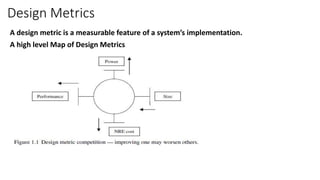
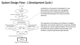
Digital System Design
(ELEC-03772)
Fall 2023- Batch 2020
Digital Design Methods, Constraints, Parameters and models
Types of Digital System Implementations
• Processor Based Systems
• General purpose processor based Systems
• Special processor based systems
• Micro controller based systems
• Embedded Systems with software modules
• FPGA Based Systems
• ASICs
Design Vs Analysis
Analysis:
- To find outcomes of a
given circuit.
- Circuit performs 4 Bit
Addition
- Single Answer
- How much current this
circuit draws
Design:
- To Develop a circuit which
meets the criteria.
- Circuit SHOULD perform 4 Bit
Addition
- Constrains
- It should perform within 1ms
- Consume <1mA
- Should be adjusted in a watch
- etc
How you have been designing Digital Circuit ?
• Determine the Requirements (Adder, Mux, Counter, etc.)
• Determine the scale of circuit (inputs, Outputs etc.)
• Develop function Table
• Develop Boolean equations
• Process for Simplification
• Formation of schematic Diagram
Exceptions:
- Are you Sure that your design / Schematic is best in terms of Performance of the desired function ?
- Is your Designed Circuit best in terms of its Size ? - Does your Designed Circuit Consumes Lesser Power ?
- How Much it will Cost You?
Design Metrics
A design metric is a measurable feature of a system’s implementation.
A high level Map of Design Metrics
1- Performance:
The execution time of the system or the processing power.
- Time required to complete a task (latency or response time),
- The number of tasks that can be processed per unit time (throughput).
Factors which influence include
The clock speed, the word length, the number of general purpose registers,
the instruction variety, memory speed, programming language and  the
availability of suitable peripherals.
Example Performance Metrics
- MIPS (Million Instructions per Second)
- MFLOPS (Mega Flops- Mega Floating Point Operations per Second)
There can be many more. A designer can propose its Own
Design Metrics
The Processor Performance Equation
CPU time = CPU clock cycles for a program ∗ Clock cycle time
CPU time = IC ∗ CPI ∗ Clock cycle time  IC – Instruction Count CPI- clock /Instruction
Design Metrics - Performance
2- Power Design Metrics:
-Handheld / Mobile Devices have prompted this metric significantly due to
battery usage. Issues with Battery in terms of size / weight.
- Heat Sink for high performance electronics impact size and performance
Factors which influence include
- Clock Speed
- I/O Drive Circuits
- Operational Voltages of the system
- Standby electronic power consumption
Design Metrics
System Design Flow- ( Development Cycle )
The separation into hardware and software is designer
dependent. An example might be the conversion of (BCD)
into signals for a seven segment display. This function can
be performed using a software look-up table, or by
hardware using the appropriate logic decoder.
architecture or framework is developed in a top
down fashion. Broken down into manageable
functional elements. followed by determining
the relationships between the major functional
elements.
Design Partitioning – a technique for Hardware
The design is partitioned into a number of inherently interdependent tasks or levels of
abstractions. The levels of design abstraction start at a very high level and descend eventually
to the individual elements that need to be aggregated to yield the top level function.
Architecture Design
For example, the x86 microprocessor architecture specifies
the instruction set, register set, and memory model.
Microarchitecture design
how the architecture is partitioned into registers and functional units.
Pentium, Celeron, AMD KS, and Athlon are all microarchitectures offering
different performance / transistor count tradeoffs for the ×86 architecture.
Logic design
How functional units are constructed. For example, various logic
designs for a 32-bit adder in the x86
Circuit design
how transistors are used to implement the logic.
Physical design describes the layout of the chip
Abstraction enables designers to handle multiple levels of
implementation of a module separately.
• Gates in logic Design has concealed complexity of MOSFETs
• Block Diagram of an 8051
• Development of logic diagram of ALU
• How to develop electronic circuit which implement a gate function
• Implement the electronic circuit on Silicon
Design Abstraction
Design Methods
• Top – Bottom Approach
• Bottom Up Approach
Bottom Up
Design Flow Examples: calculator (reference: article on internet - Nijotech_vol33_no3)
Specifications:
- 4x4 key board
- Type of display
- Size
- Power supply
- Computational capacity (limited by 8 bit)
ASICs Vs FPGAs
• ASIC:
ASIC means Application Specific Integrated Circuit. It is a device that is created for a
specific purpose or functionality. They contain only one functionality in them and
through the lifetime of the chip, it can perform only that function. For example,
CPU in your phone is an ASIC. It is meant to function as a CPU for its whole life. Its
logic function cannot be changed to anything else because its digital circuitry is
made up of permanently connected gates and flip-flops on silicon.
• FPGA:
FPGA means Field Programmable Gate Array. It can be “field” programmed to work
as per the intended design. It means it can work as a microprocessor or graphics
card, or even as both at once. The designs running on FPGA’s are generally created
using hardware description languages such as VHDL and Verilog. FPGA is made up
of number of Configurable Logic Blocks (CLB’s) and are connected with
Programmable Interconnects. The CLB’s are primarily made of Look-Up Tables
(LUT’s), Multiplexers and Flip-Flops. They can implement complex logic functions.
Difference between ASIC and FPGA
ASIC FPGA
Permanent circuitry. Once the application specific circuit is
taped-out into silicon, it cannot be changed. The circuit will
work same for its complete operating life.
Reconfigurable circuit. FPGAs can be reconfigured with a
different design. They even have capability to reconfigure a
part of chip while remaining areas of chip are still working!
This feature is widely used in accelerated computing in data
centers.
Same as for FPGA. Design is specified using HDL such as
Verilog, VHDL etc.
Design is specified using HDL such as Verilog, VHDL etc.
Very high entry-barrier of cost, learning curve, liaising with
semiconductor foundry etc. Starting ASIC development from
scratch can cost well into millions of dollars.
Easier entry-barrier. One can get started with FPGA
development for as low as USD $30.
Suited for very high-volume mass production. Not suited for very high-volume mass production.
Much more power efficient than FPGAs. Power consumption
of ASICs can be very minutely controlled and optimized.
Less energy efficient, requires more power for same function
which ASIC can achieve at lower power.
ASIC fabricated using the same process node can run at much
higher frequency than FPGAs since its circuit is optimized for
its specific function.
Limited in operating frequency compared to ASIC of similar
process node. The routing and configurable logic eat up
timing margin in FPGAs.
Difference between ASIC and FPGA
ASIC FPGA
ASICs can have complete analog circuitry, for example WiFi
transceiver, on the same die along with microprocessor cores.
This is the advantage which FPGAs lack.
Analog designs are not possible with FPGAs. Although FPGAs
may contain specific analog hardware such as PLLs, ADC etc,
they are not much flexible to create for example RF
transceivers.
ASICs are definitely not suited for application areas where the
design might need to be upgraded frequently or once-in-a-
while.
FPGAs are highly suited for applications such as Radars, Cell
Phone Base Stations etc where the current design might need
to be upgraded to use better algorithm or to a better design.
It is not recommended to prototype a design using ASICs
unless it has been absolutely validated. Once the silicon has
been taped out, almost nothing can be done to fix a design
bug (exceptions apply).
Preferred for prototyping and validating a design or concept.
Many ASICs are prototyped using FPGAs themselves!
ASIC designers need to care for everything from RTL down to
reset tree, clock tree, physical layout and routing, process
node, manufacturing constraints (DFM), testing constraints
(DFT) etc. Generally, each of the mentioned area is handled
by different specialist person.
FPGA designers generally do not need to care for back-end
design. Everything is handled by synthesis and routing tools
which make sure the design works as described in the RTL
code and meets timing. So, designers can focus into getting
the RTL design done.
Design Flow: FPGA Design entry can be done using
two ways. One is through
schematic; another is through
Hardware Description Language
(HDL).
Synthesis: As the design entered is in form of
code, it needs to be converted into a actual
circuit what we intend to implement. This is
done by the synthesis tools. It converts the
behavior code into gate level netlist where the
entire circuit will be represented in form of
gates, flip-flops and multipliers. It is then
optimized by the reduction of logic, elimination
of redundant logic, and the reduction of the
size of the design while simultaneously making
it faster to implement.
Implementation: the layout of your design will be
determined and consists of three steps: translate,
map, and place & route. The tools used in this
step are provided by the FPGA vendors
The first step for the tools is to gather all the
constraints regarding the assignment and position
of the pins, maximum delay or the input period of
the clock.
Then the tool maps out the implementation by
comparing the resource requirement specified in
the files to the resources actually available on the
FPGA being used.
The circuit is divided into the logic blocks or
elements in the form of sub blocks. As a result,
your entire design is placed in specific logic blocks
and is ‘mapped out’ into the FPGA.
Program FPGA: load the mapped out and
completely routed design into the FPGA. It will
generate a Bit-Stream file and this bit stream
file will be dumped onto your FPGA board using
Flash programmer device.
ASIC Design Flow
Specification: what this chip will do?
i.e. is it a micro controller?
Architecture: what ‘blocks’ are required
to meet specifications? Estimation of area,
Cost and power consumption.
RTL Design: RTL design using HDL describes
how the data is transferred between different
components in the design.
RTL Verification: verify using test bench.
Job of verification engineers
Synthesis – generate gate level netlist
Produces netlist files
Gate Level Simulation: to boost the
confidence level of the design
Design For Test: additional modules to
conduct post production test
Floor Plan: Pin plan, power grid,
modules placements;
e.g. house architecture
Placement: optimize the floor plan
for legal assignments
Clock Tree : develop clock signals,
path from master clock,
reduces timing errors
Routing: Setting physical connections
amongst all modules
Sign-Off & Fabrication: all tests to
check specification , performance
Generate file for Fabrication
Post Silicon Validation: Testing for
Fabrication process.
Chip Packaging: Finally chip is packaged
Processor Technologies
Questions:
• Explain the need of Design Tools for Digital System Design tasks.
• Define and explain the Design Metrics, How they come in reverse
relations ? Give examples
• Explain the ‘performance’ metric for digital systems
• A numerical example in form of performance per unit time
• Explain the concept of System Design flow
• Explain the concept of system partitioning/ abstraction
• How can you compare a system developed in FPGA and ASIC?
•

module 1-2 - Design Methods, parameters and examples.pptx

  • 1.
    Digital System Design (ELEC-03772) Fall2023- Batch 2020 Digital Design Methods, Constraints, Parameters and models
  • 2.
    Types of DigitalSystem Implementations • Processor Based Systems • General purpose processor based Systems • Special processor based systems • Micro controller based systems • Embedded Systems with software modules • FPGA Based Systems • ASICs
  • 3.
    Design Vs Analysis Analysis: -To find outcomes of a given circuit. - Circuit performs 4 Bit Addition - Single Answer - How much current this circuit draws Design: - To Develop a circuit which meets the criteria. - Circuit SHOULD perform 4 Bit Addition - Constrains - It should perform within 1ms - Consume <1mA - Should be adjusted in a watch - etc
  • 4.
    How you havebeen designing Digital Circuit ? • Determine the Requirements (Adder, Mux, Counter, etc.) • Determine the scale of circuit (inputs, Outputs etc.) • Develop function Table • Develop Boolean equations • Process for Simplification • Formation of schematic Diagram Exceptions: - Are you Sure that your design / Schematic is best in terms of Performance of the desired function ? - Is your Designed Circuit best in terms of its Size ? - Does your Designed Circuit Consumes Lesser Power ? - How Much it will Cost You?
  • 5.
    Design Metrics A designmetric is a measurable feature of a system’s implementation. A high level Map of Design Metrics
  • 6.
    1- Performance: The executiontime of the system or the processing power. - Time required to complete a task (latency or response time), - The number of tasks that can be processed per unit time (throughput). Factors which influence include The clock speed, the word length, the number of general purpose registers, the instruction variety, memory speed, programming language and  the availability of suitable peripherals. Example Performance Metrics - MIPS (Million Instructions per Second) - MFLOPS (Mega Flops- Mega Floating Point Operations per Second) There can be many more. A designer can propose its Own Design Metrics
  • 7.
    The Processor PerformanceEquation CPU time = CPU clock cycles for a program ∗ Clock cycle time CPU time = IC ∗ CPI ∗ Clock cycle time  IC – Instruction Count CPI- clock /Instruction Design Metrics - Performance
  • 8.
    2- Power DesignMetrics: -Handheld / Mobile Devices have prompted this metric significantly due to battery usage. Issues with Battery in terms of size / weight. - Heat Sink for high performance electronics impact size and performance Factors which influence include - Clock Speed - I/O Drive Circuits - Operational Voltages of the system - Standby electronic power consumption Design Metrics
  • 9.
    System Design Flow-( Development Cycle ) The separation into hardware and software is designer dependent. An example might be the conversion of (BCD) into signals for a seven segment display. This function can be performed using a software look-up table, or by hardware using the appropriate logic decoder. architecture or framework is developed in a top down fashion. Broken down into manageable functional elements. followed by determining the relationships between the major functional elements.
  • 11.
    Design Partitioning –a technique for Hardware The design is partitioned into a number of inherently interdependent tasks or levels of abstractions. The levels of design abstraction start at a very high level and descend eventually to the individual elements that need to be aggregated to yield the top level function. Architecture Design For example, the x86 microprocessor architecture specifies the instruction set, register set, and memory model. Microarchitecture design how the architecture is partitioned into registers and functional units. Pentium, Celeron, AMD KS, and Athlon are all microarchitectures offering different performance / transistor count tradeoffs for the ×86 architecture. Logic design How functional units are constructed. For example, various logic designs for a 32-bit adder in the x86 Circuit design how transistors are used to implement the logic. Physical design describes the layout of the chip
  • 12.
    Abstraction enables designersto handle multiple levels of implementation of a module separately. • Gates in logic Design has concealed complexity of MOSFETs • Block Diagram of an 8051 • Development of logic diagram of ALU • How to develop electronic circuit which implement a gate function • Implement the electronic circuit on Silicon Design Abstraction
  • 13.
    Design Methods • Top– Bottom Approach • Bottom Up Approach
  • 16.
  • 18.
    Design Flow Examples:calculator (reference: article on internet - Nijotech_vol33_no3) Specifications: - 4x4 key board - Type of display - Size - Power supply - Computational capacity (limited by 8 bit)
  • 19.
    ASICs Vs FPGAs •ASIC: ASIC means Application Specific Integrated Circuit. It is a device that is created for a specific purpose or functionality. They contain only one functionality in them and through the lifetime of the chip, it can perform only that function. For example, CPU in your phone is an ASIC. It is meant to function as a CPU for its whole life. Its logic function cannot be changed to anything else because its digital circuitry is made up of permanently connected gates and flip-flops on silicon. • FPGA: FPGA means Field Programmable Gate Array. It can be “field” programmed to work as per the intended design. It means it can work as a microprocessor or graphics card, or even as both at once. The designs running on FPGA’s are generally created using hardware description languages such as VHDL and Verilog. FPGA is made up of number of Configurable Logic Blocks (CLB’s) and are connected with Programmable Interconnects. The CLB’s are primarily made of Look-Up Tables (LUT’s), Multiplexers and Flip-Flops. They can implement complex logic functions.
  • 20.
    Difference between ASICand FPGA ASIC FPGA Permanent circuitry. Once the application specific circuit is taped-out into silicon, it cannot be changed. The circuit will work same for its complete operating life. Reconfigurable circuit. FPGAs can be reconfigured with a different design. They even have capability to reconfigure a part of chip while remaining areas of chip are still working! This feature is widely used in accelerated computing in data centers. Same as for FPGA. Design is specified using HDL such as Verilog, VHDL etc. Design is specified using HDL such as Verilog, VHDL etc. Very high entry-barrier of cost, learning curve, liaising with semiconductor foundry etc. Starting ASIC development from scratch can cost well into millions of dollars. Easier entry-barrier. One can get started with FPGA development for as low as USD $30. Suited for very high-volume mass production. Not suited for very high-volume mass production. Much more power efficient than FPGAs. Power consumption of ASICs can be very minutely controlled and optimized. Less energy efficient, requires more power for same function which ASIC can achieve at lower power. ASIC fabricated using the same process node can run at much higher frequency than FPGAs since its circuit is optimized for its specific function. Limited in operating frequency compared to ASIC of similar process node. The routing and configurable logic eat up timing margin in FPGAs.
  • 21.
    Difference between ASICand FPGA ASIC FPGA ASICs can have complete analog circuitry, for example WiFi transceiver, on the same die along with microprocessor cores. This is the advantage which FPGAs lack. Analog designs are not possible with FPGAs. Although FPGAs may contain specific analog hardware such as PLLs, ADC etc, they are not much flexible to create for example RF transceivers. ASICs are definitely not suited for application areas where the design might need to be upgraded frequently or once-in-a- while. FPGAs are highly suited for applications such as Radars, Cell Phone Base Stations etc where the current design might need to be upgraded to use better algorithm or to a better design. It is not recommended to prototype a design using ASICs unless it has been absolutely validated. Once the silicon has been taped out, almost nothing can be done to fix a design bug (exceptions apply). Preferred for prototyping and validating a design or concept. Many ASICs are prototyped using FPGAs themselves! ASIC designers need to care for everything from RTL down to reset tree, clock tree, physical layout and routing, process node, manufacturing constraints (DFM), testing constraints (DFT) etc. Generally, each of the mentioned area is handled by different specialist person. FPGA designers generally do not need to care for back-end design. Everything is handled by synthesis and routing tools which make sure the design works as described in the RTL code and meets timing. So, designers can focus into getting the RTL design done.
  • 23.
    Design Flow: FPGADesign entry can be done using two ways. One is through schematic; another is through Hardware Description Language (HDL). Synthesis: As the design entered is in form of code, it needs to be converted into a actual circuit what we intend to implement. This is done by the synthesis tools. It converts the behavior code into gate level netlist where the entire circuit will be represented in form of gates, flip-flops and multipliers. It is then optimized by the reduction of logic, elimination of redundant logic, and the reduction of the size of the design while simultaneously making it faster to implement. Implementation: the layout of your design will be determined and consists of three steps: translate, map, and place & route. The tools used in this step are provided by the FPGA vendors The first step for the tools is to gather all the constraints regarding the assignment and position of the pins, maximum delay or the input period of the clock. Then the tool maps out the implementation by comparing the resource requirement specified in the files to the resources actually available on the FPGA being used. The circuit is divided into the logic blocks or elements in the form of sub blocks. As a result, your entire design is placed in specific logic blocks and is ‘mapped out’ into the FPGA. Program FPGA: load the mapped out and completely routed design into the FPGA. It will generate a Bit-Stream file and this bit stream file will be dumped onto your FPGA board using Flash programmer device.
  • 24.
    ASIC Design Flow Specification:what this chip will do? i.e. is it a micro controller? Architecture: what ‘blocks’ are required to meet specifications? Estimation of area, Cost and power consumption. RTL Design: RTL design using HDL describes how the data is transferred between different components in the design. RTL Verification: verify using test bench. Job of verification engineers Synthesis – generate gate level netlist Produces netlist files Gate Level Simulation: to boost the confidence level of the design Design For Test: additional modules to conduct post production test Floor Plan: Pin plan, power grid, modules placements; e.g. house architecture Placement: optimize the floor plan for legal assignments Clock Tree : develop clock signals, path from master clock, reduces timing errors Routing: Setting physical connections amongst all modules Sign-Off & Fabrication: all tests to check specification , performance Generate file for Fabrication Post Silicon Validation: Testing for Fabrication process. Chip Packaging: Finally chip is packaged
  • 26.
  • 27.
    Questions: • Explain theneed of Design Tools for Digital System Design tasks. • Define and explain the Design Metrics, How they come in reverse relations ? Give examples • Explain the ‘performance’ metric for digital systems • A numerical example in form of performance per unit time • Explain the concept of System Design flow • Explain the concept of system partitioning/ abstraction • How can you compare a system developed in FPGA and ASIC? •

Editor's Notes

  • #3 For example, one of the promising digital signal processors, which was used to implement MPEG based video codec could only process still monochrome images of resolution 512 × 512 pixels at one frame per second instead of the required frame rate of 30. In contrast to this, the hardware implementations based on FPGAs and ASICs can exploit pipelining and massively parallel processing resulting in faster and cost effective designs. ASIC designs are suitable if high-volume production is envisaged. However, in the research and development phase and for rapid prototyping of a new design, FPGA is the right choice