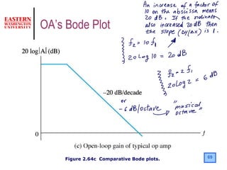
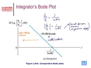
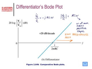
1. Operational amplifiers are widely used electronic components that can perform mathematical operations such as amplification, integration, differentiation, and summation.
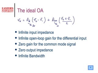
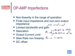
2. An ideal op-amp has infinite input impedance, infinite gain, zero output impedance, and can operate at infinite bandwidth.
3. Op-amps are used in various circuit configurations including inverting amplifiers, non-inverting amplifiers, summing amplifiers, voltage followers, and filters.