Downloaded 179 times
![EC 707 Advanced communication Laboratory Dept. of Electronics & Communication Engineering
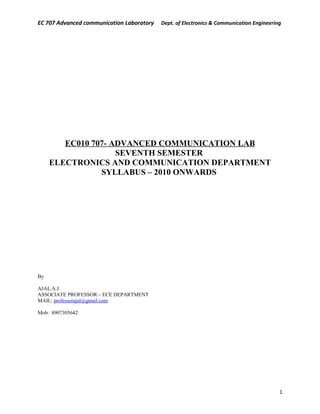
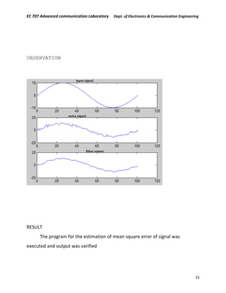
%Input signal
f=1000;
t=0:0.00001:0.001;
X_Tra= 10*sin(2*pi*f*t);
% Adding White Gaussian noise by the channel
SNR=0.01;
X_Noise=AWGN(X_Tra,SNR);
% plot(X_Noise);
X_Rec=X_Noise;
%Cost = (Received signal - Estimated signal).^2
Error_UnCor = sum((X_Rec - X_Tra).^2)/N;
X_Fil= filter([0.33 0.33 0.33],1,X_Rec);
% plot(X_Fil);
Error_Cor=sum((X_Fil - X_Tra).^2)/N;
figure;
subplot(311);
plot(X_Tra);
subplot(312);
plot(X_Rec);
subplot(313);
plot(X_Fil)
14](https://image.slidesharecdn.com/baskgenerator-150725063358-lva1-app6891/85/Advanced-communication-lab-manual-14-320.jpg)
![EC 707 Advanced communication Laboratory Dept. of Electronics & Communication Engineering
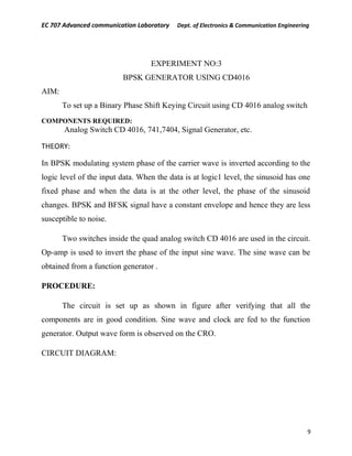
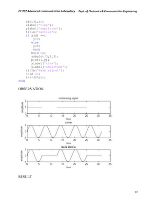
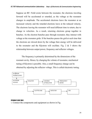
EXPERIMENT NO:5
BINARY AMPLITUDE SHIFT KEYING
AIM:
To generate Binary amplitude shift keyed (BASK) signal using MATLAB
THEORY:
Generation of BASK Amplitude shift keying - BASK - is a modulation
process, which imparts to a sinusoid two or more discrete amplitude levels. These
are related to the number of levels adopted by the digital message. For a binary
message sequence there are two levels, one of which is typically zero. The data
rate is a sub-multiple of the carrier frequency. Thus the modulated waveform
consists of bursts of a sinusoid. One of the disadvantages of BASK, compared with
FSK and PSK, for example, is that it has not got a constant envelope. This makes
its processing (eg, power amplification) more difficult, since linearity becomes an
important factor. However, it does make for ease of demodulation with an
envelope detector.
Program:
clc
clear all
a=input('enter the binary sequence');
l=length(a);
i=0;
for d=1:l
i=i:.01:i+(2*pi);
subplot(3,1,1);
plot(i,a(d));
ylim ([0 2])
xlabel('time');
ylabel('amplitude');
title('modulating signal');
hold on;
c=sin(i);
subplot(3,1,2);
16](https://image.slidesharecdn.com/baskgenerator-150725063358-lva1-app6891/85/Advanced-communication-lab-manual-16-320.jpg)

The document outlines the syllabus and experiments for the EC 707 Advanced Communication Laboratory course in the Electronics and Communication Engineering department. It details various experiments involving modulation techniques such as BASK, BFSK, and BPSK using analog switches, as well as MATLAB experiments for signal processing and microwave experiments to study klystron characteristics, frequency and wavelength measurements, and VSWR. Each experiment includes the aim, required components, theoretical background, procedures, and expected results.


